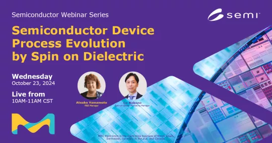
October 23, 2024
Sponsored by the Electronics business of Merck KGaA, Darmstadt, Germany
Time
10:00 am - 11:00 am CEST
Location
Germany
Semiconductor Device Process Evolution by Spin on Dielectric
This webinar is the 8th in a series exploring trending topics integrated solutions materials and semiconductor development, co-hosted with the Electronics business of Merck KGaA, Darmstadt, Germany.
Join us to discover how Spin-on Dielectrics (SOD) materials and processes contributed to advanced semiconductor device manufacturing, and new material development to overcome future device challenges.
During this interactive webinar, you will gain insights into the unique aspects of the SOD process and materials, the benefits Merck KGaA, Darmstadt, Germany, offers to customers, and the latest developments designed to meet future technical demands. Additionally, Merck KGaA, Darmstadt, Germany, will share more on their dedicated application lab's capabilities in supporting customers.
Even if you cannot attend the live session, don’t worry, by registering you will have access to the on-demand video to watch the webinar at your convenience.
Who should attend?
- Processes and tool engineers of lithography, thin film deposition, CMP, etc.
- Material technology management teams.
- Supply Chain, Procurement, Process, and Technology Development professionals in semiconductor companies.
Why attend?
The Semiconductor Materials Series attracts professionals, business and technology leaders, researchers, academics, and industry analysts from across the global electronics supply chain. In this webinar, you will gain practical insights on:
- Unique aspects and benefits of SOD materials and processes in semiconductor manufacturing.
- New SOD materials and processes development to help solve customer’s future technical demands.
- Merck KGaA, Darmstadt, Germany, capability to support customers with a dedicated application lab.
Register today to access exclusive content during an interactive session.
You will be able to apply innovative techniques and best practices to solve your unique challenges.
Live Q&A will follow.
Attendees are invited to submit questions ahead of time at [email protected].
Agenda
Welcome Remarks

Presentations
Biography
Atsuko Yamamoto is the manager of R&D in Semiconductor Materials leading the polymer research program of the Spin-On Dielectric R&D group. After joining the company in 1998, she worked as an R&D scientist of photoresist for TFT arrays, technical marketing for photo patterning materials for packaging applications in semiconductor markets and Si-based materials for optoelectronic applications. She led the R&D team in Japan and successfully launched new products as Head of display materials R&D. She is based at the R&D and manufacturing site in Kakegawa, Shizuoka-Pref. Japan.
Biography
Go Nakano is a Spin-on Global Marketing Manager focusing on new product development marketing of Spin-on dielectric for advanced memory and logic devices manufacturing. With more than 30 years of combined business and technical expertise in electronics-related fields, Go Nakano has a proven record of accomplishment as Head of Strategic Marketing of Display Patterning Materials, successfully led new product introduction, and expanded market share in existing products. He is based in Tokyo, Japan.
Live Q&A and Conclusions
Sponsors