
Exhibitor Services

Exhibitor Guide
Digital Library

2026 Exhibitors
Booth options
Booth price:
SEMI member: 3,995 EUR
Non-SEMI member: 4,495 EUR
Package Rate (3D + APC* 50% off): 5,995 EUR
Prices in EUR (net), excl. 19% German VAT.
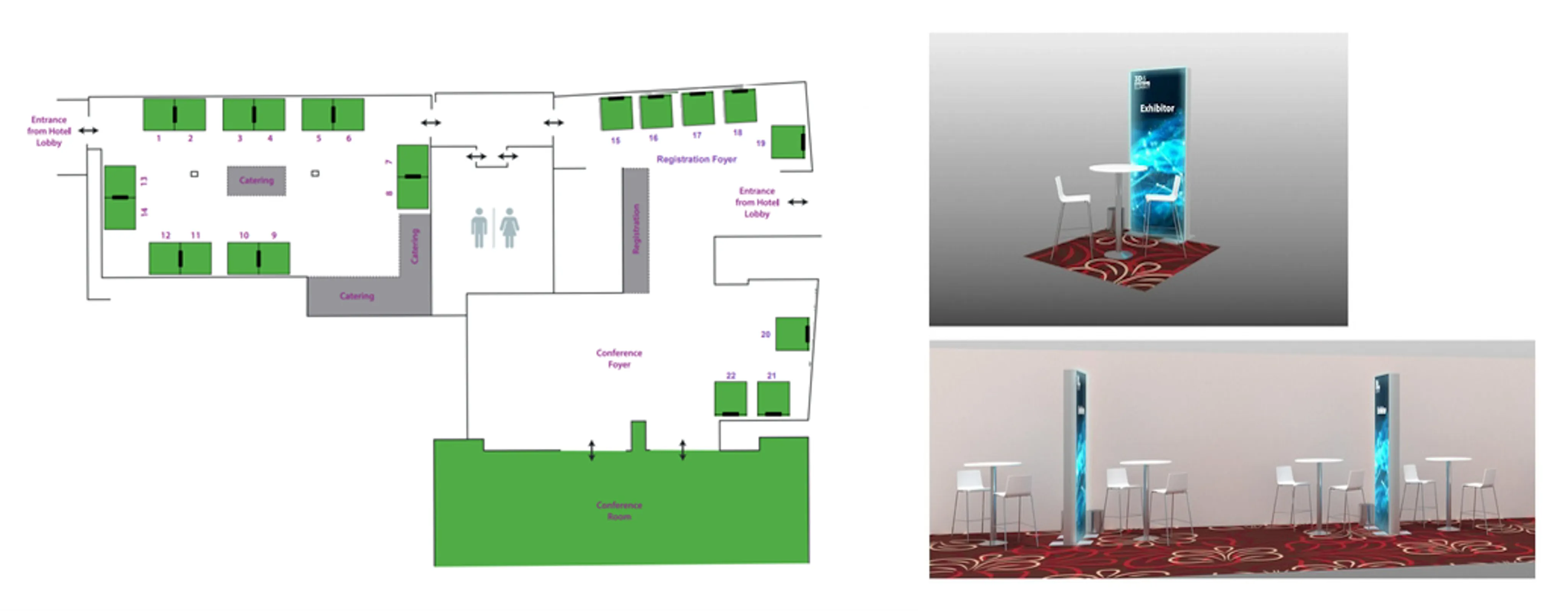
Exhibition Package
Secure a turnkey presence at the event with our Exhibition Package, designed to deliver maximum visibility with minimal setup effort. The package includes one fully equipped modular booth and one full-access Delegate Pass to the 3D & Systems Summit, granting access to the exhibition floor, conference sessions, and the exclusive networking dinner cruise.
The 2×2m modular booth is delivered ready-to-use. It includes illuminated branded graphics, furniture, power supply, and essential onsite services—allowing you to focus entirely on engaging with decision-makers and industry peers.
As an added exhibitor benefit, one additional Delegate Pass may be purchased at a 20% discounted rate.
💡 Special Package Rate available:
A limited, attractive combined package rate is available, bringing together a booth at the 3D & Systems Summit and a special exhibition presence at the Advanced Packaging Conference (APC).
Advanced Packaging Conference (APC)
📅 November 11, 2026
📍 Munich ICM
Co-located with SEMICON Europa & electronica
👉 For full specifications, current floor plan, booth availability, and details of this exclusive combined Package Rate, please download the EXHIBITION Package PDF.


Exhibitor Information
3DiS Technologies
3DiS Technologies offers 3D integration and 3D packaging solutions based on its innovative 3D interconnection technologies. By leveraging the third dimension, the company’s cutting-edge technologies enable miniaturization of electronic systems and passive devices while improving their performance.
Website - 3DiS Technologies
Adeia Inc.
Adeia (Nasdaq: ADEA) is the technology company known for developing foundational innovations that enable next-generation solutions for the semiconductor and media industries. We invent and license foundational technologies that shape the future of digital entertainment, electronics, and high-performance computing. Our portfolio transforms technologies into an experience that is intelligent, immersive, and personal. For more information, please visit our website.
Website - Adeia
ASE
ASE, Inc. is the leading global provider of semiconductor manufacturing services in assembly and test. With world-class leadership in heterogeneous integration, manufacturing efficiency, and sustainability initiatives, packaging innovation is at the core of ASE capabilities. Today, ASE’s advanced packaging, system-in-package, and chiplet solutions are accelerating compute momentum across AI, HPC, Data Center, Automotive, IoT, 5G, and more. To learn about our latest technology advances, including our VIPack™ and powerSiP™ platforms as well as our industry-first automated 310mm × 310mm panel-level packaging production line, please visit our website or follow us on LinkedIn and X: @aseglobal.
Website - ASE
ASMPT
ASMPT SEMI is the leading provider of forward-looking solutions for advanced packaging and semiconductor assembly. With its commitment to innovation and customer satisfaction, ASMPT SEMI offers a comprehensive range of products and services that meet the evolving needs of the microelectronics industry. Expert knowledge covers areas such as flip-chip and wafer-level packaging, advanced interconnect technologies, and more. ASMPT SEMI’s state-of-the-art solutions enable customers to achieve higher performance, greater reliability, and improved cost-efficiency in the manufacturing of their semiconductor devices.
ASMPT SEMI sees itself as a pioneer and driving force of the Intelligence Revolution. With its advanced packaging and assembly technologies, the business segment creates the invisible connections that enable intelligent applications in Artificial Intelligence, Smart Mobility, and Hyperconnectivity.
Website - ASMPT
Carl Zeiss Microscopy Deutschland GmbH
ZEISS is the only manufacturer worldwide offering light, X-ray, electron, and ion beam microscopy from a single source. With the most comprehensive imaging portfolio in the industry, ZEISS delivers cutting-edge solutions across the entire semiconductor value chain—from wafer fab to packaging and assembly. For mask making and lithography, ZEISS enables zero-defect strategies, in-die metrology, and precise overlay control. Its process control and failure analysis tools provide actionable insights to meet the challenges of next-gen semiconductor devices. Globally active ZEISS combines innovation with reliability in optical excellence.
www.zeiss.com/semiconductor-microscopy
www.zeiss.com/semiconductor-manufacturing-technology
Website - Zeiss
Comet AG
Comet is a leading global provider of high-end X-ray-based system solutions for non-destructive materials testing in the semiconductor, electronics, automotive, and aerospace industries, as well as for research facilities and scientific institutions. Comet Yxlon inspection solutions help users ensure the quality of their products, optimize their manufacturing processes, and thus increase efficiency and productivity.
The high-precision computed tomography systems for use in the laboratory support research and development and enable detailed structural analysis, metrology applications, and simulation models. The precise microfocus tubes reveal minute details of modern electronic components in the semiconductor and electronics industries.
Website - Home page - Comet
Confovis
Confovis, based in Jena, Germany, develops and manufactures high-precision Automated Optical Inspection (AOI) and optical 3D surface metrology systems for semiconductor applications. Since 2009, we have delivered customer-specific solutions for photonics, MEMS, 3DIC, and advanced packaging.
Our WAFERinspect platform uses proprietary area-scanning Structured Illumination Microscopy for non-contact, high-resolution 3D measurements with outstanding stability, repeatability, and accuracy. In the same optical path, image-based defect inspection with multiple wavelengths enables flexible detection, classification, and dimensional analysis. GUI-based AI tools support fast recipe creation and automated defect classification.
Website - Confovis
FAMES Pilot Line
The FAMES Pilot Line pioneering initiative promotes semiconductor technologies in Europe by supporting the emergence of higher-performance, more energy-efficient, and more sustainable chip designs. The objectives of the FAMES Pilot Line are to establish a domestic semiconductor Pilot Line for cutting-edge microelectronic technologies in Europe, and provide open access to this Pilot Line to stakeholders of the electronic value chain. These objectives are aligned with those of the EU Chips Act: bolster the EU semiconductor industry and support European technological sovereignty through innovations, facilitated access to R&D, and training.
Website - Fames Pilot Line
Forschungsfabrik Mikroelektronik Deutschland (FMD)
The Research Fab Microelectronics Germany (FMD) is a cooperation between 13 Fraunhofer Institutes and the two Leibniz institutes FBH and IHP. It serves as the central point of contact for all matters related to micro- and nanoelectronic research and development in Germany and across Europe. As a one-stop shop, FMD brings together advanced technologies and system solutions from its cooperating institutes to provide a customized, comprehensive portfolio. Established within FMD’s shared virtual framework in 2017, this joint research cooperation has grown into one of the largest of its kind, now comprising more than 5,400 employees and a uniquely broad range of expertise and infrastructure. Since 2024, FMD has been a registered trademark of the Fraunhofer-Gesellschaft.
Website - FMD - Forschungsfabrik Mikroelektronik Deutschland, 3D-Showroom
Fraunhofer IZM-ASSID
Fraunhofer IZMs “All Silicon System Integration Center Dresden – ASSID” was established in 2010 and is celebrating its 15th anniversary in 2025. It is an integral part of Fraunhofer IZM's wafer-level system packaging and system integration. ASSID operates a state-of-the-art 300mm process line for 3D wafer-level system integration based on Cu-Through Silicon Via technology. Constituent parts of the line are individual process modules for TSV formation, TSV post-processing, assembly, and 3D stacking. This enables application-oriented development of 3D wafer-level processes, qualification, and prototype manufacturing for 3D wafer-level systems in packages. Key application areas include High Performance & Quantum Computing, Edge Sensor Systems, etc.
Website - Fraunhofer
Hamamatsu Photonics Deutschland GmbH
Hamamatsu Photonics is one of a few companies in the world that develops a wide range of light sensors, such as photodiodes, image sensors and photomultiplier tubes, as well as light sources, both narrow bandwidth and broadband types.
Our portfolio of more than 10,000 products not only includes components, but also fully integrated systems, for example, emission microscopes with laser stimulation options for failure analysis, substrate thickness monitoring systems, plasma process monitors for advanced control of etching processes and imaging systems for electro- and photoluminescence analysis of photovoltaic devices. Furthermore, we offer X-ray sources, X-ray detectors and cameras for integration into inspection tools.
Website - Hamamatsu
Kistler Instrumente AG
Kistler is the global market leader for dynamic pressure, force, torque and acceleration measurement technology. Unique sensor technology from this Swiss corporation helps to shape future innovations not only in automotive development and industrial automation but also in many newly emerging sectors. The focus is on issues such as electrified drive technology, autonomous driving, emission reduction and Industry 4.0. Some 2,000 employees at more than 60 facilities across the globe are dedicated to the development of new solutions, and they offer application-specific services at the local level. Ever since it was founded in 1959, the Kistler Group has grown hand-in-hand with its customers and in 2024, it posted sales of mCHF 448.
Website - Measurement systems and sensors | Kistler
Lam Research
Semiconductor breakthroughs start here.
We combine superior systems engineering, technology leadership, and a commitment to customer success to advance the global semiconductor industry.
Lam Research Corp. (NASDAQ: LRCX) is a trusted global supplier of innovative wafer fabrication equipment and services to the semiconductor industry. Our broad portfolio of market-leading deposition, etch, strip, and wafer cleaning solutions helps customers achieve success on the wafer by enabling device features that are 1,000 times smaller than a grain of sand—it’s why nearly every chip today is built with Lam technology. Our strong values-based culture fuels our progress, and it’s through collaboration, precision, and delivery that we are driving semiconductor breakthroughs that define the next generation.
Let’s prove it.™
Website - Lam Research
LPKF Laser & Electronics SE
Innovative manufacturing technologies for growth markets
The LPKF Group (LPKF) is an international technology company specializing in innovative, laser-based manufacturing solutions for demanding industries. The company is a leader in the development of high-tech solutions that address aspects such as precision, energy efficiency, and sustainability in particular.
In the 50 years of the company’s history, LPKF has established leading positions in a number of highly specialized market segments. With its patented LIDE (Laser Induced Deep Etching) technology for high-precision glass processing, LPKF is tackling a key need in the semiconductor industry and consistently expanding its strong position with a growing portfolio of solutions.
Website - LIDE® Laser Induced Deep Etching Technology | LPKF
NanoIC Pilot Line
The NanoIC pilot line is a pioneering European initiative, hosted by imec, set to provide a leading-edge beyond 2nm System-on-Chip (SoC) pilot line for advanced logic, memory, and interconnect technologies. The project aims to drive European technology leadership across critical markets such as computing, communication, mobility, energy and health. The pilot line is a collaboration between imec, CEA-Leti, Fraunhofer-Gesellschaft, VTT, CSSNT-UPB, and Tyndall Institute and is supported by the Chips Joint Undertaking, through the European Union’s Digital Europe (101183266) and Horizon Europe programs (101183277), as well as by the participating states Belgium (Flanders), France, Germany, Finland, Ireland and Romania. For more details, please visit nanoic-project.eu.
Website - Home | NanoIC pilot line
Plasmatreat
Plasmatreat is a global leader in plasma surface treatment systems, offering Openair‑Plasma® for atmospheric pressure and AURORA‑Plasma for low‑pressure applications. Both enable precise cleaning and activation of surfaces and ensure stable conditions for subsequent processes. PlasmaPlus® additionally allows functionalization through defined nanocoatings. The technologies are used across industries such as electronics, automotive, medical, packaging, and energy across the value chain to prepare surfaces for bonding, painting, printing, or sealing. As a dry process, plasma reduces chemicals and environmental impact. Plasmatreat operates technology centers worldwide and a global sales and service network in over 30 countries.
Website - Plasmatreat
Precitec Optronik GmbH
Precitec 3D Metrology is a German manufacturer of innovative sensors and optical probes. The CHRocodile® product line sets the standard for contact-free thickness and distance measurements in semiconductor applications. It enables precise measurement of structures, thickness, bow, and warp from the sub-micron to micron range. High measurement rates support efficient data acquisition.
The sensors can be used standalone or integrated into production equipment for inline metrology. With extensive semiconductor experience, Precitec provides customized solutions and test measurements. Proven worldwide, CHRocodile® sensors are widely used in quality control.
Advantages:
• Surface-independent measurements
• High axial resolution
• Works on tilted, reflective surfaces
• Small spot size
• Compact, robust design
Website - Precitec Optronik GmbH
SEMI Europe
SEMI Europe is the European arm of SEMI® , the global industry association connecting over 3,000 member companies and 1.5 million professionals worldwide across the semiconductor and electronics design and manufacturing supply chain. We accelerate member collaboration on solutions to top industry challenges through Advocacy, Workforce Development, Sustainability, Supply Chain Management, and other programs. Curious about where the semiconductor market is heading? Visit our booth to learn more about our data platforms and forecast reports and see how they support confident, forward-looking decision-making.
Website - Market Data Reports | SEMI
SEMILAB
SEMILAB provides advanced metrology solutions, both in-line and R&D, for semiconductor device manufacturers. With its 45 product lines and 300+ unique products, Semilab offers a comprehensive suite of optical and electrical metrology solutions designed to ensure precision, reliability and efficiency and address the growing challenges of 3D structures, thin films, and advanced materials, helping advance the rapidly evolving field of Semiconductor Advanced Packaging and Panel Level Packaging.
Semilab’s metrology solutions provide advanced measurement capabilities for layer thickness, critical dimensions, defect detection, resistance and numerous other applications, ensuring optimal performance at the critical steps of the packaging process.
Website - Semilab
SET – Smart Equipment Technology
SET (Smart Equipment Technology) is a world-leading supplier of high-accuracy Flip-Chip Bonders. Since 1975, we have designed and manufactured leading-edge semiconductor equipment for high-precision applications.
We support laboratories and semiconductor companies seeking world-class precision and superlative reliability in the assembly of their components. With our Flip-Chip Bonders installed worldwide, SET’s equipment is globally renowned for unsurpassed sub-micron accuracy and incomparable flexibility.
Ranging from manual-loading to fully-automated solutions, our Flip-Chip Bonders cover a wide range of bonding applications and possess the unique ability to handle and bond fragile and/or small components onto substrates up to 300 mm.
Website - SET – Smart Equipment Technology
Syenta
Syenta introduces Localized Electrochemical Modeling (LEM), a high-speed metallization technology that extends Semi-Additive manufacturing to 1 µm and below. LEM combines localized electrodeposition with micron-resolution stamp-based patterning to enable precise, additive fabrication of redistribution layers (RDLs) and microbumps.
The company was founded in 2022 as a spin-off from The Australian National University, and has its HQ and R&D team in Sydney, Australia.
Website - Syenta
X-FAB Silicon Foundries SE
X-FAB MEMS Foundry is part of the X-FAB Group, the world’s leading analog/mixed-signal foundry, with more than 25 years of experience in integrating a wide range of functionalities such as non-volatile memory, optical sensors, MEMS, and high-voltage transistors. In addition to a broad portfolio of modular CMOS processes with geometries ranging from 0.35 to 0.11 micrometers, X-FAB offers specialized technologies such as SOI, silicon carbide (SiC), and MEMS processes. As a leading MEMS foundry, X-FAB MEMS Foundry provides process technologies for manufacturing micromechanical sensors for detecting pressure, acceleration, rotation, and infrared radiation, among others. It also offers integrated solutions where MEMS sensors are combined with CMOS circuits. In this context, comprehensive solutions for heterogeneous integration (HI) are offered or developed upon customer request for SoC and SoP applications. In Germany, X-FAB currently employs around 1,300 highly qualified staff. Worldwide, approximately 4,500 employees work for the company. Sales offices in key countries across Asia, Europe, and the USA ensure close contact with customers around the globe.
Website - X-FAB
W. L. Gore & Associates
Gore delivers advanced material solutions that support a cleaner, more efficient semiconductor ecosystem. Our innovative portfolio spans key manufacturing stages—from lithography and wafer cleaning to SoC testing. We offer ultra-flexible cables and cable assemblies, microfiltration membranes, and ozonation modules engineered for purity, durability, and reliability. Our MEMS Protective Vents provide robust environmental protection with excellent gas permeability and acoustic transparency. With decades of materials science expertise, Gore is a trusted partner to semiconductor manufacturers worldwide.
Website - Gore
Wooptix
Wooptix is a semiconductor wafer metrology innovator that provides the fastest, most accurate in-line measurements with the highest lateral resolution. Through its use of wavefront phase imaging (WFPI), a proprietary technique derived from research in adaptive optics, its systems measure the shape, nanotopography, and roughness of the entire silicon wafer in a single shot. It is actively deploying solutions at various customer sites across Asia, Europe, and North America.
Together with their resistance to vibrations and ease of adapting to the user’s needs, they are valuable systems for measuring the wafer shape and nanotopography in a single shot.