downloadGroupGroupnoun_press release_995423_000000 copyGroupnoun_Feed_96767_000000Group 19noun_pictures_1817522_000000Member company iconResource item iconStore item iconGroup 19Group 19noun_Photo_2085192_000000 Copynoun_presentation_2096081_000000Group 19Group Copy 7noun_webinar_692730_000000Path
Skip to main content
Default Banner Image

Malaysia

Martinez, CA—EUV Tech (EUVT), a global leader in designing and manufacturing at-wavelength EUV metrology equipment, is excited to announce the release of the FALCON Photoresist Flood Exposure Tool. As our next-generation EUV resist characterization and diagnostics tool, FALCON allows photoresist manufacturers to rapidly and accurately test EUV resist sensitivity, as well as providing patterning materials developers critical insights into exposure mechanisms.

Built upon EUV Tech’s proven resist tool technology, FALCON is a fully automated tool that supports high-throughput contrast curves on EUV-patterning materials and radiation chemistry diagnostics by integrating a wide variety of optional add-on analysis and processing modules.

Enhancing FALCON’s platform is an array of in-situ analysis and process modules, including Fourier Transform Infrared (FTIR) Spectroscopy, Atomic Mass Spectrometry, Total Electron Yield (TEY), Photo-Electron Spectroscopy (PES), environmental and vacuum bake module with additional diagnostics, and a scanner-environment exposure module.

Key to FALCON’s effectiveness is its highly uniform exposure spot size of 6 mm, supporting high-sensitivity chemical analysis and over 1,000 exposures for a 300 mm wafer in a single recipe run. Built-in data visualization tools make it possible to analyze this rich data. Combining uniformity, high configurability, and deep data collection and analysis makes FALCON a highly efficient, cost-effective tool for advanced photoresist development.

For more information on the enhanced FALCON Flood Exposure Tool or any of EUV Tech’s at-wavelength metrology tools, please visit euvtech.com.

About EUV Tech
EUV Tech enables technology advancement in the frontiers of semiconductor manufacturing and material science through the development of world-leading EUV and soft-x-ray instrumentation and techniques.

For further information, contact:
EUV Tech, Inc.
[email protected]
+1 (925) 229-4388

Nordson Electronics Solutions, a global leader in reliable electronics manufacturing technologies, has developed several solutions for panel-level packaging (PLP) during semiconductor manufacturing. In one particular case, Nordson’s customer, Powertech Technology, Inc. (PTI) saw underfill yields improve to greater than 99% as they plan to transition from wafers to panels in their manufacturing operations. For details about this solution developed in late 2024 and 2025, download the case study here: Customer Success: Powertech Technology Inc. (PTI) Advances Panel Level Packaging with Nordson.

PTI, one of the world’s top OSAT (Outsourced Semiconductor Assembly and Test) companies, worked with the Nordson applications team to set up a comprehensive PLP demonstration that achieved high-quality, void-free underfill results at scale, using the industry-leading ASYMTEK Vantage® Series fluid dispensing system, equipped with the ASYMTEK IntelliJet® Jetting system. Nordson’s precision technology mitigated warpage and optimized fluid flow while decreasing cycle time by almost 30%.

PLP offers a path to managing the complexity of larger die sizes and higher-density designs while maintaining manufacturability and cost efficiency as the semiconductor industry transitions from 300-mm wafers to panels. PTI is enabling PLP applications that are designed to meet the semiconductor industry’s growing demands to serve AI, high-performance computing (HPC), and chiplet-based architectures.

Underfill has been pivotal in semiconductor packaging since the adoption of flip-chips in the 1990s. As applications have become more demanding, particularly in high-performance CPUs, GPUs, and advanced architectures like flip-chip and 2.5D/3D ICs, the importance of underfilling to enhance mechanical reliability and thermal performance has grown. Since the beginning, Nordson developed innovations for underfill processes as the industry evolved from PC board, substrate, wafer, and now panel applications.

Nordson’s distributor, Jetinn Global Equipment Ltd., supported the advancements discussed in this case study by investing in demonstration equipment and providing expert technical support.

Penang, Malaysia – June 2025 – ViTrox aims to be the World’s Most Trusted Technology Company, proudly shares that our Co-Founder, Mr. Steven Siaw, was honoured with the SEMI Southeast Asia Industry Tribute Award on May 20, 2025, in conjunction with the 30th anniversary of SEMI Southeast Asia.

This award honours 30 distinguished leaders from the region’s semiconductor and microelectronics sectors who have made significant contributions to the industry’s growth and development. Mr. Steven was recognised for his exceptional leadership, integrity, and consistent business growth over the years, along with his passion for mentoring young talents and driving positive impact in areas such as innovation, sustainability, and community building.

"Receiving this award is truly an honour. It represents not just my journey, but the collective efforts of our amazing ViTrox team and partners who have believed in our mission. I’m truly humbled and grateful to be part of such a dynamic industry. I look forward to continuing my journey — serving, growing, and giving back to the semiconductor community.” — Mr. Steven Siaw.

This milestone stands as a testament to his enduring impact and aligns with ViTrox’s broader purpose of contributing to the advancement of society and the well-being of humankind through compassionate innovations. With cutting-edge technologies, a bold vision, and a passion for excellence, ViTrox is poised to redefine industry standards and drive transformative change on a global scale.

About ViTrox Technologies
ViTrox is committed to being the World’s Most Trusted Technology Company and the leading solutions provider by integrating ViTrox's technologies, people, and strategic alliances to provide its customers with the most innovative, advanced, and cost-effective machine vision solutions of excellent quality.

ViTrox offers a full spectrum of solutions, ranging from Middle & Back-end Semiconductor Vision Solutions, SMT PCB Assembly Inspection Solutions, Integrated Industrial Embedded Solutions, and Manufacturing Intelligence Solutions Toward Industry 5.0. ViTrox is headquartered in Penang, Malaysia, with offices in Asia, Germany, and the United States and sales and support sites worldwide.

For more information about ViTrox’s products and services, please visit www.vitrox.com.

Belgium China France Germany India Ireland Italy Japan Malaysia Russia Singapore South Korea Taiwan United States Vietnam Webinar-Critical Minerals-v1_360x317_Event_Calendar_CM Business Executive Technical
Highlighted content

As world leaders act to secure access to these minerals, companies come under pressure to follow due diligence guidelines to promote ethical sourcing of these materials for their supply chains.  Regulations such as the US Dodd-Frank Wall Street Reform and Consumer Protection Act (Section 1502), EU Regulation 2017/821 and the EU Corporate Sustainability Due Diligence Directive require companies to trace materials through their supply chains and report to the public about their use of conflict minerals. 

Several industry associations, including the Responsible Business Alliance’s Responsible Minerals Initiative, were created to help companies with their due diligence efforts. Reports such as those issued by the US Government Accountability Office on Conflict Minerals offer insights into the efficacy of these regulations and suggest improved approaches for industry engagement. 

The SEMI Responsible Supply Chain (RSC) working group was recently formed to host discussions on these topics. This webinar will provide insights from speakers Jennifer Peyser, Responsible Business Alliance Senior Vice President of Responsible Sourcing, and Kimberly Gianopoulos, Managing Director for the International Affairs and Trade team at the U.S. Government Accountability Office (GAO).

United States

8:00 am - 8:05 am
Kim Harrison
Dr. Kimberly Harrison, Ph.D
Senior MEMS Engineer
AMFitzgerald & Associates

Welcome and Introductions of RSC working group

Dr. Harrison is a MEMS Engineer with AMFitzgerald & Associates, a design firm located in the Bay Area California. She has a doctoral degree in mechanical engineering from Stanford University, and has worked as a designer and process engineer in the semiconductor industry for 10 years. She was nominated as a 2022 MEMS & Sensors Industry Group Emerging Leader. As a founding member and leader of the SEMI Responsible Supply Chain Working Group, she hopes to bring SEMI members together to discuss solutions to human rights issues in the semiconductor supply chain.

Conflict Minerals Supply Chain Overview

8:05 am - 8:35 am
Kimberly Gianopoulos
Managing Director for the International Affairs and Trade
U.S. Government Accountability Office (GAO)

Report Review

Director Gianopoulos oversees a 140-person team that reviews a wide variety of federal government oversight issues, including International Security Assistance, Bilateral and Multilateral Foreign Assistance, International Trade and Finance, and U.S. Diplomatic Presence and Management. She serves as a facilitator in GAO’s Learning Center and participates in recruiting activities. Ms. Gianopoulos has received several awards, including a Distinguished Service Award, a Meritorious Service Award, a Client Service Award, and several Results Through Teamwork awards. Ms. Gianopoulos earned a Bachelor’s degree in Mathematics and a Master’s degree in Public Analysis and Administration from the State University of New York at Binghamton. She is a Certified Government Financial Manager and a member of Pi Alpha Alpha, the Global Honor Society for Public Affairs and Administration.

Jen Peyser
Jennifer Peyser
Executive Director
Responsible Minerals Initiative

RMI Activity Overview

“The RMI supports over 500 downstream, midstream, and upstream member companies with a suite of due diligence standards and tools, data, guidance, training, and other resources for global responsible sourcing and regulatory compliance. Our facility and supply chain due diligence standards are rooted in longstanding international norms while reflecting emerging corporate and stakeholder priorities for regulatory compliance, managing sustainability risks and impacts, and fostering responsible mineral supply chains.”

8:35 am - 8:55 am

Q&A

8:55 am - 9:00 am

Summary and Closing Remarks

SCM 8:00 am - 9:00 am Off Add to Calendar 2025-07-09 08:00:00 2025-07-09 09:00:00 Critical Minerals, Due Diligence and the Semiconductor Supply Chain United States SEMI.org [email protected] America/Los_Angeles public America/Los_Angeles Register for On-demand
Event format
Promote in calendar
Off
Belgium France Germany Ireland Italy Japan Malaysia Singapore South Korea Taiwan United States Vietnam Image Business Training Featured Speakers

Leverage SEMI U learning offerings to wrap up your 2025 professional development journey! Our pledge remains unwavering: providing comprehensive, technical education to equip you with the skills needed for a prosperous journey in the semiconductor sector.

Are you ready to take your semiconductor industry knowledge to the next level? We're thrilled to invite you to our upcoming webinar titled "SEMI University - 2025 and beyond." This webinar promises to be an informative session where you'll gain insights into the latest updates, exciting live trainings at SEMICON West and virtually the remainder of this year and beyond. 

During this webinar, you can expect to:  

  • Discover the latest updates and enhancements to SEMI U's course catalog.  
  • Learn about the exciting live, in-person training courses scheduled for SEMICON West.
  • Review upcoming virtual instructor-led trainings.
  • Gain access to a special 10% discount on ALL on-demand courses.  


United States

Headshot of Naresh Naik
Naresh Naik
Director, SEMI University
SEMI
SEMI U Workforce Development

Join us to discover our current course offerings, upcoming in-person and virtual trainings, and more. Engage in a Q&A session. Plus, by attending this free webinar, you'll receive a 10% discount code for all on-demand courses and will be entered into a raffle to win a FREE course bundle ($100 value). 

Choose your session:

8:00 am - 8:30 am Off Add to Calendar 2025-09-25 08:00:00 2025-09-25 08:30:00 SEMI University - 2025 & Beyond Join us to discover our current course offerings, upcoming in-person and virtual trainings, and more. Engage in a Q&A session. Plus, by attending this free webinar, you'll receive a 10% discount code for all on-demand courses and will be entered into a raffle to win a FREE course bundle ($100 value). Choose your session:US/EU: 8:00 AM – 8:30 AM PT [Register Now]Asia/US: 5:00 PM – 5:30 PM PT [Register Now] United States SEMI.org [email protected] America/Los_Angeles public Register Now
Event format
Promote in calendar
Off

Nijmegen, The Netherlands, 14 May 2025 — Trymax Semiconductor Equipment (Trymax), a leading provider of plasma- and UV-based solutions for semiconductor manufacturing, announces the installation of its 500th process chamber in Asia. This milestone reflects continued momentum across key regional markets—including China, Taiwan, South Korea, Malaysia, and the Philippines—and signals strong progress toward the company’s goal of 1,000 global installations by the end of 2025.

“Reaching 500 installations in Asia is a significant milestone for Trymax,” said Peter Dijkstra, Chief Commercial Officer at Trymax Semiconductor Equipment. “It reflects our team’s dedication to delivering practical, high-performance solutions with the speed and reliability that our customers need in order to stay competitive.”

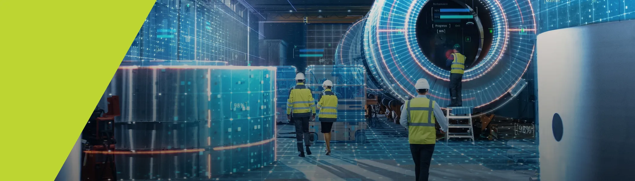
Responsiveness as a Competitive Edge

In an industry where uptime, productivity, and reliability are critical, Trymax has earned a reputation for being highly responsive—from the inquiry stage to post-installation support. The company’s nimble structure allows it to take action quickly and decisively, enabling customers to manufacture with confidence. Many partners have cited the ease of communication with Trymax, and the timely support received, as reasons for early and continued engagement.

Supporting Asia’s Semiconductor Surge

Asia continues to lead global semiconductor growth, driven by accelerated adoption in high-demand sectors. Customers across the region are pushing forward with innovation and scale, particularly in:

• Automotive: The transition from internal combustion engine (ICE) vehicles to electric vehicles (EVs) is reshaping the industry. EVs require significantly more semiconductors—often up to 3,000 chips per vehicle—due to greater electrification, power management, and onboard computing systems. This shift is fueling demand for reliable, high-throughput semiconductor processing solutions.

• Artificial Intelligence (AI): The rise of AI and machine learning applications—from data centers to edge devices—is creating a surge in demand for advanced microprocessors and high-density memory. Backend processes play a critical role in ensuring the performance and yield of these complex chips, making equipment reliability and process control essential.

• 5G & Connectivity: Asia’s rapid deployment of 5G networks, combined with its mobile-first population and high-volume data consumption, is pushing the limits of semiconductor performance. This growth requires advanced packaging technologies, faster interconnects, and increased wafer-level precision—all of which depend on stable, repeatable backend processing steps.

Trymax’s plasma and UV curing technologies are designed to meet these demands, delivering proven results in ashing, descum, surface cleaning and activation, and isotropic etching. With a strong footprint across the region, the company continues to support customers at the forefront of innovation.

Forward Plans and Strategic Vision

To support its continued growth in Asia and globally, Trymax is advancing several strategic initiatives. The company is exploring plans to establish local manufacturing in China, a move aimed at strengthening supply chain resilience and improving responsiveness to regional customer needs.

As part of its 2025–2030 roadmap, Trymax is also deepening its collaborations with leading semiconductor manufacturers. By taking on selective, non-core process steps—particularly those related to backend wafer processing—Trymax helps larger players free up internal resources and maintain operational focus where it matters most.

In parallel, Trymax is expanding its role in advanced packaging. As integrated circuit (IC) designs evolve toward increasingly complex multi-layered stacks—sometimes comprising up to 16 layers—ensuring pristine, activated surfaces between each layer is critical. Trymax’s plasma solutions are engineered to meet these exacting standards, enabling customers to maintain high yield and reliability in next-generation device architectures.

Meet Trymax at SEMICON Southeast Asia 2025

Trymax will be showcasing its latest plasma-based innovations at SEMICON Southeast Asia 2025, from 20–22 May at the Sands Expo and Convention Centre, Marina Bay Sands, Singapore. Attendees are invited to meet the Trymax team at Booth #B1633 to learn more about the company’s technology roadmap and expansion plans.

###

About Trymax Semiconductor Equipment

Trymax’s core business is to support semiconductor manufacturers through the world with innovative plasma-based solutions for photoresist removal, surface cleaning, isotropic etch, as well as UV curing and charge erase applications, that are used in the fabrication of integrated circuits and other semiconductor devices. Trymax is a privately held company headquartered in Nijmegen, The Netherlands. Trymax operates regional sales and service offices in Europe, UA, China, Southeast Asia, Taiwan, and Japan.

Learn more at www.trymax-semiconductor.com.

Test Research, Inc. (TWSE: 3030), the leading test and inspection systems provider for the electronics manufacturing industry, is proud to announce its successful partnership with Bosch in the development of an AI visual check solution for MEMS packaging.

Bosch has recognized TRI's valuable contribution to their success in MEMS packaging in 2025 with a Certificate of Appreciation. The certificate acknowledges the successful completion of the AI visual check for MEMS packaging, highlighting the strong cooperation and partnership between the two companies.

This collaboration demonstrates TRI's expertise in AI-driven inspection solutions and its commitment to providing valuable solutions for the electronics manufacturing industry. TRI's AI-powered solutions include the AI Defect Detection, AI Smart Programming, AI Verify Host, AI training tool, AI Station, and more.

Please visit the following link to learn more about TRI's AI Solutions:
https://www.tri.com.tw/en/about/about-107-2-2.html

Learn more about the Bosch Group by following the link below:
https://www.bosch-presse.de/pressportal/de/en/company-page.html

###

About Test Research, Inc. (TRI)

TRI (TWSE: 3030), offers the most robust product portfolio in the industry for Automatic Test and Inspection solutions. Learn more at http://www.tri.com.tw. For sales and service information, please write to us at [email protected] or call +886-2-2832 8918.

Stanton Chase is pleased to announce that Sundar Rajan Ramalingam has joined the firm as a Partner in North America. His addition strengthens the firm's executive search and leadership consulting capabilities for the semiconductor sector at a time of rapid transformation.

Sundar brings nearly three decades of leadership experience across manufacturing and global technology sectors. He has scaled a multi-billion-dollar global engineering division and supported the growth of several Global Capability Centers (GCCs). Within the semiconductor ecosystem, he has played a pivotal role in building and advising leadership teams across chip design, chip-to-cloud platforms, semiconductor fabs, and foundry operations.

This deep operational and strategic background gives Sundar a unique perspective on the evolving talent needs of semiconductor organizations.

"The semiconductor industry is entering a pivotal era—what I call a 'perfect leadership storm'—driven by generative AI, strategic autonomy imperatives, and breakthroughs like 3nm and advanced packaging," said Sundar. "While these trends are accelerating innovation, the industry also faces a growing talent gap. Companies need capable leaders who can navigate complexity, scale innovation, and build resilient teams. I plan to use my experience in technology and manufacturing to help semiconductor companies find executives who deliver results and foster sustainable growth."

Sundar's career spans both strategic HR leadership and general management with P&L responsibility, offering clients a rare blend of technical insight and leadership development expertise.

"Sundar fits well with our North American team and fills a specific need in our practice," said Mickey Matthews, Managing Director at Stanton Chase in North America and Chair of the Governance Committee. "His time working across borders gives him a genuine understanding of how global teams function. Blending this multicultural understanding with Sundar's deep technology products and services vertical expertise matters a lot to the clients we serve and specifically in the semiconductor space."

Jan-Bart Smits, Managing Partner at Stanton Chase Amsterdam and Global Sector Leader for Semiconductors, added: "Sundar joins us when the semiconductor industry sits at a turning point. Firms in this sector are looking for something different in their executives—people who understand both market forces and engineering details. Sundar knows this world and will further enhance our ability to serve chip makers and their suppliers."

As the semiconductor industry moves into a new chapter—marked by AI-driven demand, geopolitical shifts, and the race toward next-gen nodes—Sundar's appointment signals Stanton Chase's commitment to helping clients lead with confidence and clarity.

Sundar holds an MBA from XLRI Jamshedpur (India) and completed executive education programs, including the Chief Human Resource Officer Program at Wharton, University of Pennsylvania.

He will serve clients from Stanton Chase offices in Baltimore and Raleigh, USA, as well as Bangalore, Hyderabad, and Chennai, India—locations near semiconductor business centers.

Click here to learn more about Sundar.

Click here to learn more about Stanton Chase's semiconductor expertise.

About Stanton Chase

Stanton Chase ranks among the top global retained executive search firms with more than 76 offices in 45 countries and a worldwide team of senior consultants. Stanton Chase serves clients across multiple industry specialties and places C-suite executives, senior managers, and board members for companies ranging from global corporations to emerging businesses. Stanton Chase belongs to the Association of Executive Search and Leadership Consultants (AESC), adhering to the highest industry standards of professionalism and ethics.

Belgium China France Germany India Ireland Italy Japan Malaysia Singapore South Korea Taiwan United States Vietnam Register Now Scope 3.11 800x800 Business Executive
Highlighted content

The webinar will address the following:

  1. Overall Contents of the Guidance
  2. Topics explored in creating the Guidance
  3. Intention of why the Guidance was developed
  4. Who was involved in the development
  5. Who should use the Guidance
  6. How it differs from existing standards and protocols

United States

Sustainability

Join the Leaders of the Semiconductor Climate Consortium Scope 3 Working Group, plus other industry experts, to review the recently released Scope 3 Category 11 GHG Assessment and Guidance for the Semiconductor Value Chain.  Compiled with the expert assistance of ERM, with input from all levels of the ecosystem, this document has been designed to align on reporting Scope 3, Category 11, an important step in measuring the impact of reduction efforts across the industry.

Download the Guidance Document

8:00 am - 9:00 am Off Add to Calendar 2025-06-12 08:00:00 2025-06-12 09:00:00 Webinar - Category 3.11 Review Join the Leaders of the Semiconductor Climate Consortium Scope 3 Working Group, plus other industry experts, to review the recently released Scope 3 Category 11 GHG Assessment and Guidance for the Semiconductor Value Chain.  Compiled with the expert assistance of ERM, with input from all levels of the ecosystem, this document has been designed to align on reporting Scope 3, Category 11, an important step in measuring the impact of reduction efforts across the industry.Download the Guidance Document United States SEMI.org [email protected] America/Los_Angeles public America/Los_Angeles
Event format
Promote in calendar
Off

Singapore, May 12, 2025 - DuPont (NYSE: DD) is excited to announce its participation in SEMICON Southeast Asia (SEMICON SEA), taking place May 20-22, 2025, in Singapore. At booth L3105, DuPont will showcase the latest offerings of Kalrez® perfluoroelastomer parts specifically designed for semiconductor and electronics applications, aimed at enhancing manufacturing efficiency and operational sustainability.

“Our new Kalrez® product offerings are engineered for enhanced sealing performance, significantly reducing leaks and pumping times,” said Dr. Meredith Dunbar, Kalrez® Global Technology Leader, DuPont. “In our continuous pursuit of sustainability, we have achieved improvements in sealing performance under harsh process conditions, which enable substantial waste reduction. These advancements make Kalrez® seals an ideal choice for the toughest challenges in semiconductor fabs, and also showcase our dedication to delivering high-quality, efficient, and environmentally responsible solutions.”

Highlighting this longstanding commitment to innovation, the Kalrez® brand is proud to celebrate its 50th anniversary this year. This milestone reflects five decades of excellence and dedication to developing high-performance sealing solutions tailored for critical applications in demanding environments. At this year’s SEMICON SEA exhibition, attendees will discover several key advancements, including:

Kalrez® Bonded Door Seal (BDS): Specifically designed for semiconductor manufacturing equipment, including applications like plasma etching, CVD, and PVD, Kalrez® BDS offers improved sealing performance over conventional O-rings by reducing particle generation, extending seal life, and minimizing maintenance downtime.

Bonding Methodology: An innovative bonding method developed by DuPont's technology team, allowing Kalrez® components to be fused with other functional materials, creating unique, composite-structured Kalrez® parts.

Custom Shaped Parts: Kalrez® custom perfluoroelastomer parts can be tailored to unique geometries for specific sealing applications and are available in various shapes and compounds to meet different thermal, chemical, and plasma resistance requirements. Custom parts can be produced as both volume production and prototypes.

DuPont is proud to be driving technological advancements in the Kalrez® product family and providing game-changing solutions to its customers worldwide. All SEMICON SEA attendees are invited to join in celebrating the 50th anniversary of Kalrez® and explore how Kalrez® products can support their innovation programs.

For more information about Kalrez® parts and applications, please visit www.kalrez.com.

About DuPont

DuPont (NYSE: DD) is a global innovation leader with technology-based materials and solutions that help transform industries and everyday life. Our employees apply diverse science and expertise to help customers advance their best ideas and deliver essential innovations in key markets, including electronics, transportation, construction, water, healthcare, and worker safety. More information about the company, its businesses, and solutions can be found at www.dupont.com. Investors can access information included on the Investor Relations section of the website at investors.dupont.com.

#   #   #

05/12/25

DuPont™, the DuPont Oval Logo, and all trademarks and service marks denoted with ™, ℠ or ® are owned by affiliates of DuPont de Nemours, Inc. unless otherwise noted. 

For further information, contact:

Rebekah Lazar
Semiconductor Technologies Communications Leader
DuPont
[email protected]

Cell: +1-302-509-1859