downloadGroupGroupnoun_press release_995423_000000 copyGroupnoun_Feed_96767_000000Group 19noun_pictures_1817522_000000Member company iconResource item iconStore item iconGroup 19Group 19noun_Photo_2085192_000000 Copynoun_presentation_2096081_000000Group 19Group Copy 7noun_webinar_692730_000000Path
Skip to main content
Default Banner Image

France

Registration

SEMI Members:  $49

Use your corporate email address during log in to be recognized as a SEMI Member.

Non-Members:  $99

Students:  Free

Contact Gity Samadi ([email protected]) with a picture of your student ID to receive your discount code.

Belgium France Germany Ireland Italy United States FEMC 20 tile with NBMC Recording.jpg Business Executive
Highlighted content

As artificial intelligence (AI) continues to transform the MedTech and semiconductor landscapes, it brings forth a myriad of opportunities and challenges that demand careful attention to governance and  compliance.  In this webinar, Jenny Colgate, an experienced intellectual property, privacy, and data governance lawyer, will share her expertise and insights on implementing effective AI governance frameworks including: (1) an introduction to AI governance; (2) the evolving AI and privacy regulatory landscape; (3) ethical considerations and best practices; (4) establishing an AI governance program for your organization; and (5) follow-through and enforcement.

ABOUT THE SPEAKER:

Jenny Colgate is an experienced litigator whose expertise extends into all facets of intellectual property and technology-related matters, including patents, data protection, trade secret, unfair competition, trademark, copyright, breach of contract, and fraud claims. Jenny works across many subject areas, including artificial intelligence, healthcare, semiconductors, software, and consumer products. In addition to Jenny’s litigation practice, she also regularly counsels clients on AI governance programs, IP protection and enforcement, privacy law compliance and best practices, and contract/licensing issues.  A recognized thought leader, Jenny routinely authors expert analyses and speaks on panels and webinars. Jenny has a B.A. from University of Pennsylvania (summa cum laude, with honors), an L.L.M. in intellectual property from University of New Hampshire Franklin Pierce Law center (magna cum laude), and a J.D. from University of New Hampshire Franklin Pierce Law Center (magna cum laude). Jenny is a certified CIPP/US privacy professional and has completed the IAPP AI Governance Professional training program.

United States

Jenny Colgate
Jenny Colgate
Partner
Rothwell Figg
Gity Samadi
Gity Samadi
Director, R&D Programs
SEMI
NBMC FlexTech Off Add to Calendar Disabled Register Now
Event format
Belgium China France Germany India Ireland Italy Japan Malaysia Russia Singapore South Korea Taiwan United States Vietnam 360x317_Event_Calendar_Ad_GenAI_v1@2x Business Executive Technical
Highlighted content

Generative artificial intelligence (GenAI) applications are becoming increasingly popular and with new model and applications being currently launched every day. However, GenAI applications are very compute intensive requiring specialized servers and chips.

In this webinar, panelists will discuss different adoptions scenarios and their implications on the semiconductor industry. In particular, they will dive deep on the need for additional manufacturing capacity for logic and memory as we expect the biggest investment needs there.

You will also hear from the CEO of SEMI on the potential AI holds for the semiconductor industry, along with SEMI's ongoing efforts to address this transformative technology.

United States

8:00 am - 8:10 am

Opening Remarks

8:10 am - 8:15 am

SEMI Smart Data-AI Initiative

8:15 am - 8:25 am

Semiconductor Industry Outlook Driven by GenAI

8:25 am - 8:35 am

Silicon Demand Forecast and Scenarios

8:35 am - 8:50 am

Implication for the Ecosystem

8:50 am - 9:00 am

Q & A

Explore the surge in GenAI applications and their impact on the semiconductor industry, including discussions on adoption scenarios and the need for increased manufacturing capacity, with insights from SEMI's CEO on AI's potential and SEMI's proactive strategies.

Off Add to Calendar 2024-06-18 00:00:00 2024-06-18 00:00:00 GenAI – the next S-curve for the semiconductor industry? Explore the surge in GenAI applications and their impact on the semiconductor industry, including discussions on adoption scenarios and the need for increased manufacturing capacity, with insights from SEMI's CEO on AI's potential and SEMI's proactive strategies. United States SEMI.org [email protected] America/Los_Angeles public America/Los_Angeles Register Now
Event format

HATFIELD, Pa. (USA), APRIL 18, 2024 — Brooks Instrument, a world leader in advanced flow measurement and control, has acquired Creative Machining Technology of Corona, California. The acquisition took place April 1, 2024, under Illinois Tool Works (ITW), Brooks Instrument’s parent company.

Creative Machining Technology (CMT) provides a variety of machining and manufacturing services, ranging from individual part production through end-item manufacturing, kitting and assembly.

The company has long been a key supplier to Brooks Instrument, with core competencies rooted in high-precision CNC machining. CMT has proven expertise manufacturing and polishing ultrahigh-purity components with extremely tight tolerances for demanding applications, including semiconductor manufacturing.

“By integrating Creative Machining Technology into Brooks Instrument, we are enhancing our in-house expertise for critical machined components and machining capabilities, which adds to our supply chain assurance for producing ultrahigh-purity instruments,” said Brent Best, Vice President and General Manager — Brooks Instrument Semiconductor Division, an ITW Company. “In addition, we’ve increased our capabilities for quick-turn customer R&D requests to create more innovative flow measurement and control solutions.”

CMT has extensive experience manufacturing to tolerances as tight as 0.0001". This proficiency and CMT’s manufacturing facilities will enable Brooks Instrument to more quickly and effectively design and produce complex wetted flow path components for the company’s industry-leading mass flow controllers (MFCs). MFCs are the most important element in the gas delivery systems used for semiconductor manufacturing. In addition, CMT has both Class 1,000 and Class 10,000 clean rooms for processing and handling extremely delicate electronic components that require a controlled environment.

“This acquisition is part of our strategic approach to grow our business and position us for long-term success in the semiconductor market as we ramp up to meet anticipated growth in this segment,” said Best. “Moving forward, we are excited to have CMT join Brooks Instrument as we focus on continuous improvement, growing our technology offerings and meeting our customers’ needs.”

The CMT acquisition is the latest in Brooks Instrument’s initiatives to serve the semiconductor industry. Earlier this year the company launched a new GF120xHT Series mass flow controller for high-temperature environments, while last year opened a new manufacturing site in Malaysia to expand production and partnership opportunities with key customers in the Asia-Pacific region.

For more information about Brooks Instrument’s full range of capabilities for the semiconductor industry, visit www.brooksinstrument.com/en/markets/semiconductor-manufacturing.

About Brooks Instrument
Since 1946, Brooks Instrument has been a leader in precision fluid measurement and control technology. Providing instrumentation for flow, pressure and vapor delivery, the company serves customers in semiconductor and high-tech manufacturing, laboratories and other processes and industries. With manufacturing, sales and service locations in the Americas, Europe and Asia, Brooks Instrument has the world’s largest installed base of mass flow controllers.

For more information, please visit www.BrooksInstrument.com. The company is also on LinkedIn (www.linkedin.com/company/Brooks-Instrument) and YouTube (www.youtube.com/user/Brooks407).

Belgium France Germany Ireland Italy United States CLimate Risk Webinar Business Executive
Highlighted content

The SEMI Sustainability Initiative Environmental Risk Mitigation and Reporting (ERMR) working group has been meeting for a year to collaborate on how companies in our industry should respond to the realization of our impact on climate and the growing need for reporting. The ERMR teamed up with Nasdaq to benchmark the industry using Nasdaq's Nasdaq Sustainable Lens™, an AI-powered ESG intelligence platform, to analyze and assess the maturity level of each segment of the semiconductor value chain based on publicly available sustainability and climate information of 100 leading semiconductor companies against TCFD recommendations. 


The study identifies strengths, gaps and challenges faced by the industry in implementing recommendations of the Taskforce on Climate-related Financial Disclosures (TCFD). It also offers recommendations on industry best practices to enhance climate disclosure maturity.  Download the report here.

United States

9:00 am - 9:05 am
Mousumi Bhat
Mousumi Bhat, PhD
Vice President
SEMI Sustainability

Introduction

9:05 am - 9:20 am
Alua Suleimenova
Leader, ERMR WG
Alua Suleimenova
Senior Sustainability Program Manager
Marvell

Environmental Risk Mitigation and Reporting in the Semiconductor Industry

9:20 am - 9:30 am
Michael Stiller
Michael Stiller
New Growth Initiatives
Nasdaq

How Nasdaq Benchmarked our Industry

9:30 am - 9:40 am
Jami Haaning
Jami Haaning
ESG Director
Lam Research

Lam Research – TCFD-aligned Governance Structure Supports Net Zero Goals

9:40 am - 9:50 am
Mark Didden ASML
Mark Didden
Senior Manager Sustainability Strategy
ASML

ASML – Climate Scenario Analysis Helps to Prepare Business for Climate Risk

9:50 am - 10:00 am

Questions & Answers

Sustainability

SEMI and Nasdaq are pleased to present this webinar featuring the 5 key takeaways from the recently-released report:  A Rising Tide: Building a Climate-Resilient Semiconductor Value Chain (to be linked to download page).  The report spotlights the maturity of the semiconductor value chain as it moves toward greater climate resilience and develops climate risk mitigation strategies.


The webinar features the authors and contributors to the report in a conversation about the status of the industry's outlook on its climate resilience, including case studies with companies analyzing and reporting on their positions.  


If you are responsible for or contribute to your company's risk analysis or mitigation strategies, join us for this opportunity to learn how others are approaching this topic, as well as new AI tools to make your job easier

9:00 am - 10:00 am Off Add to Calendar Disabled America/Los_Angeles Register Now
Event format
Belgium France Germany Ireland Italy 360x317_Event_Calendar_Ad_SU_OverviewSemiManu_v2 Business Technical
Highlighted content

Learning Objectives:

  • Gain a comprehensive understanding of the semiconductor industry and the manufacturing process, design and eco-system of the semiconductor industry and understand the jargon, tools, and materials used in the design and fabrication of an IC
  • Effectively be able to communicate semiconductor manufacturing concepts with other associates and industry professionals

Who Should Attend:

  • New personnel entering the field
  • Any one wanting an understanding of semiconductor manufacturing

Course Topics:

  • Basic electronics and microelectronics terms and definitions
  • Microelectronics and the role of integrated circuits
  • Define process nodes : explanation of process nodes and how they relate to device performance and cost
  • Device physics and transistor operation: understanding of the physical principles behind device operation and the functioning of transistors
  • Crystal growth and wafer prep: overview of crystal growth techniques used in semiconductor manufacturing
  • Explanation of wafer preparation techniques and materials used
  • FDSOI, fin fets, gate all around (GAA) transistors
  • Circuit design and layout
  • Mask making techniques and materials used in lithography
  • Clean rooms
  • Lithographic techniques
  • Plasma etch, wet etch and cleaning processes
  • Ion implantation
  • Diffusion techniques
  • RTP, CVD, ALD, ALE techniques and their impact on device performance
  • Electro-plating, sputtering
  • Testing
  • Wire bonding
  • Packaging techniques
  • Metrology tools and applications
  • The major players in the semiconductor ecosystem

Instructor:

Denny headshot

Denny Frye 

Course Instructor

PT International, LLC

Biography


Germany

- Workforce Development

The purpose of this course will provide a comprehensive understanding of the semiconductor industry and the manufacturing process of an integrated circuit (IC). The course is designed for new personnel entering the field or individuals who are looking for a well-rounded understanding of all the jargon, tools, and materials used in the IC manufacturing process.

Limited time offer!

  • Members: $995 $795
  • Non-members: $1095 $895
  • Students/Veterans: $895 $695

* For group orders with 10+ attendees, and for Students/Veterans discounted pricing, please contact [email protected]

Off Add to Calendar 2024-06-18 00:00:00 2024-06-19 00:00:00 Overview of Semiconductor Manufacturing Webinar (EU) The purpose of this course will provide a comprehensive understanding of the semiconductor industry and the manufacturing process of an integrated circuit (IC). The course is designed for new personnel entering the field or individuals who are looking for a well-rounded understanding of all the jargon, tools, and materials used in the IC manufacturing process.Limited time offer!Members: $995 $795Non-members: $1095 $895Students/Veterans: $895 $695* For group orders with 10+ attendees, and for Students/Veterans discounted pricing, please contact [email protected] Germany SEMI.org [email protected] Europe/Berlin public Europe/Berlin Register Now
Event format
Belgium France Germany Ireland Italy 360x317_Event_Calendar_Ad_SU_IntroSemiconductorDesign_EU_v1@2x Business Technical
Highlighted content

To meet the projected worldwide demand for semiconductor devices, the semiconductor industry is demanding technical and non-technical staff and personnel to be well versed in the key elements of integrated circuit (IC) fabrication and design. By taking this course, participants will learn how integrated circuits are designed and fabricated. Essential knowledge for non-technical professionals working in the industry will be obtained. This has been a popular training among those working in our field. In fact, over 120,000 people have taken this course since 1978!

Learning Objectives:

  • Review of the semiconductor industry and technology in laypeople terms. 
  • Understand the basics of semiconductor devices and how they work.
  • Identify the processing technologies and the equipment used to produce them, materials used, and circuit design techniques.

Who Should Attend:

  • New employees in:
    • Manufacturing
    • Engineering
    • Finance
    • Sales
    • Marketing
    • Semiconductor tool personal
    • Material suppliers
    • Training
    • Operators
    • Customer service
    • Attorneys
  • Anyone wanting a basic understanding of the semiconductor industry.  

Course Topics: 

  • Electronic fundamentals
  • Crystal growth and wafer types (Si, SiGe, SOI, SiG, SiC, GaAs)
  • Transistor types such as (bipolar, nMOS, pMOS, CMOS, bi-CMOS, FitFet, Gate All Around transistors)
  • High-k and low-k materials
  • Metal gates and High k gate oxide
  • Basic design and layout concepts
  • Mask making, wafer processing, materials used for fabricating the wafer, tools used for processing the wafer, contamination control, clean room standards, test, assembly, packaging, metrology
  • Various types of semiconductor devices and applications such as memories, MEMS, microprocessors, DSP, analog and power ICs, Etc. 

Instructor:
 

Denny headshot

Denny Frye 

Course Instructor

PT International, LLC

Biography


Germany

Workforce Development

Discover the essential secrets behind semiconductor devices! Dive into the intricate world of integrated circuit fabrication and design with our comprehensive course. Ideal for both technical and non-technical professionals, this training has been a cornerstone for the industry for over four decades, attracting over 120,000 eager learners since 1978. Join us and equip yourself with the vital knowledge needed to thrive in the semiconductor industry.

Limited time offer!

  • Members: $845 $645
  • Non-members: $945 $745
  • Students/Veterans: $745 $545

* For group orders with 10+ attendees, and for Students/Veterans discounted pricing, please contact [email protected]

9:30 am - 5:30 pm Off Add to Calendar 2024-06-17 09:30:00 2024-06-17 17:30:00 Introduction to Semiconductor Design and Fabrication for Non-Techies Webinar (EU) Discover the essential secrets behind semiconductor devices! Dive into the intricate world of integrated circuit fabrication and design with our comprehensive course. Ideal for both technical and non-technical professionals, this training has been a cornerstone for the industry for over four decades, attracting over 120,000 eager learners since 1978. Join us and equip yourself with the vital knowledge needed to thrive in the semiconductor industry.Limited time offer!Members: $845 $645Non-members: $945 $745Students/Veterans: $745 $545* For group orders with 10+ attendees, and for Students/Veterans discounted pricing, please contact [email protected] Germany SEMI.org [email protected] Europe/Berlin public Europe/Berlin Register Now
Event format

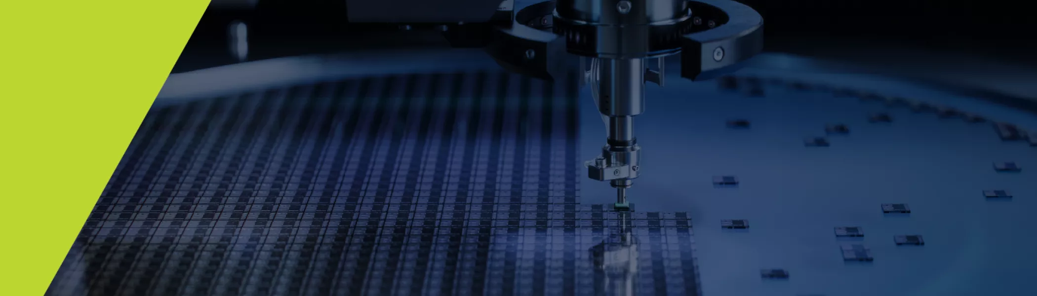
Brewer Science is the first and only company in the semiconductor industry with GreenCircle Certification.

Rolla, Mo.– April 3, 2024–Brewer Science, a global technology leader, is pleased to announce it has earned Zero Waste to Landfill Certification for the ninth consecutive year. The Zero Waste to Landfill Certification represents Brewer Science’s commitment to the responsible management of end-of-life materials and demonstrates the company’s commitment to waste diversion practices.

Brewer Science is the first and only company in the semiconductor and microelectronics industry to achieve GreenCircle Certification – Zero Waste to Landfill. GreenCircle certifies an organization for Zero Waste to Landfill Certification if 100% of the materials leaving the facility are intended to be diverted from landfill via one of GreenCircle’s acceptable means of diversion. Waste diversion from landfill, defined as the prevention and reduction of generated waste through source reduction, recycling, reuse, or composting, has been characterized as one of the best ways manufacturing companies can demonstrate genuine environmental responsibility.

Sustainability continues to be a prominent focus for Brewer Science, with remarkable progress towards goals, including:

• Net Zero Carbon Footprint by 2050
• Reduce Scope 1 and Scope 2 GHG emissions by 80% from baseline 2018 by 2030
• Divert over 75% of hazardous waste volume to re-use applications annually
• Achieve 100% renewable energy consumption annually

Education continues to play an important role in advocating for sustainable development across the supply chain. Brewer Science has developed a new program aimed at bridging the gap in environmental initiatives among its stakeholders. You can find the Sustainability Outreach Program at the bottom of Brewer Science’s Going Green webpage.

Brewer Science provides a comprehensive evaluation of the company’s five impact areas in its annual Impact Report, which can also be found on the Going Green page.

“The Sustainability Outreach Program we are launching this year is designed to work with our partners, whether that be our employees, suppliers, customers, or other organizations in the communities in which we serve, to collaborate and align on sustainability programs and projects to have a net positive impact on the environment,” states Matthew Beard, Executive Director, Strategic Planning, Management Systems, and Sustainability at Brewer Science.

For semiconductor companies, it is essential to evaluate the materials used in manufacturing, identify any more environmentally friendly alternatives, and handle the waste responsibly. Brewer Science established its Green Chemistry Program in 2019, which is an effort to identify chemical alternatives that are proven to be more sustainable, as well as divert hazardous materials for reuse applications. Additionally, Brewer Science organizes an annual community collection recycling program partnering with waste disposal companies and volunteer crews to prevent community e-waste from becoming a part of a landfill. The company shares about its sustainability programs on its “Going Green” page to encourage other tech companies to adopt more sustainable practices.

About Brewer Science
Brewer Science is a global leader in developing and manufacturing next-generation materials and processes that foster the technology needed for tomorrow. Since 1981, we’ve expanded our technology portfolio within advanced lithography, advanced packaging, smart devices, and printed electronics to enable cutting-edge microdevices and unique monitoring systems for industrial, environmental, and air applications. Our relationship-focused approach provides outcomes that facilitate and deliver critical information. Our headquarters are in Rolla, Missouri, with customer support throughout the world. We invite you to learn more about Brewer Science at www.brewerscience.com.

About the GreenCircle Certified, LLC
GreenCircle Certified, LLC was established to ensure specificity in third-party certification after encountering many unsubstantiated claims in the marketplace. Since 2009, GreenCircle has offered forward-thinking companies a competitive advantage by providing specific, third-party certification of environmental claims. GreenCircle’s rigorous evaluation process provides independent verification that claims of sustainable aspects of products and operations are valid. Manufacturers, suppliers, regulators, occupants, and consumers can be assured that products labeled with the GreenCircle Certified mark have been thoroughly assessed and their claims verified to applicable standards. Learn more at www.greencirclecertified.com/.

Kitchener, Ontario, April 2, 2024 – The SEMI North America Information and Control Committee (I&CC) has announced that Albert Fuchigami, a Senior Standards Specialist at PEER Group®, has been confirmed as a Technical Committee co-chair during its recently held spring meeting.

As an I&CC co-chair, Fuchigami will help coordinate the various SEMI task forces responsible for the development and maintenance of communication and control SEMI Standards used to automate the semiconductor manufacturing process. Fuchigami will also play an important role in facilitating collaboration between the regional technical committees while providing mentorship and guidance on navigating SEMI rules and regulations.

“I greatly appreciate the support from committee members to confirm me as co-chair,” says Fuchigami. “SEMI I&C Standards are essential to satisfy our industry’s ever growing demands for big data, smart manufacturing, and automation in an efficient and scalable manner. I look forward to helping move their development further in this role.”

Fuchigami is heavily involved in the SEMI Standards Program in North America, Japan, Taiwan, South Korea, and China. He co-leads the SEMI North America Data Diagnostic Acquisition (DDA) Task Force, has authored various SEMI articles and tech briefs, and regularly shares his knowledge and expertise at industry conferences and events.

In recognition of his contributions to the international SEMI Standards program, Fuchigami was awarded the North American SEMI International Standards Leadership Award in 2022 and the Japan Information and Control Technical Committee Award in 2021.

About PEER Group
PEER Group® is the largest supplier of innovative factory automation software products for the semiconductor industry. Since 1992, our solutions have helped the world’s most advanced OEMs and factories reduce time to market and lower costs by solving their equipment automation, data management, and process control problems. An award-winning company, PEER Group’s commitment to quality has been recognized by Intel’s EPIC Supplier Program, naming PEER Group a Distinguished Supplier in 2024. Follow PEER Group on LinkedIn.

Brewer Science is one of only 27 Distinguished Award recipients across Intel’s global supply chain.

Rolla, MO, March 28, 2024 – Brewer Science is proud to announce that it has earned Intel’s EPIC Distinguished Supplier Award. Through its dedication to Excellence, Partnership, Inclusion, and Continuous (EPIC) quality improvement, Brewer Science has achieved a level of performance that consistently exceeds Intel’s expectations.

“As one of the 27 Distinguished Supplier Award recipients in 2024, Brewer Science stands out among suppliers in Intel’s trusted supply chain,” said Keyvan Esfarjani, chief global operations officer at Intel. “Through their relentless drive to improve, they have achieved a level of performance that consistently exceeds Intel’s expectations and serves as a benchmark across the ecosystem.”

The Intel EPIC Distinguished Supplier Award recognizes a consistent level of strong performance across all performance criteria. Of the thousands of Intel suppliers around the world, only a few hundred qualify to participate in the EPIC Supplier Program. The EPIC Distinguished Award is the second-highest honor a supplier can achieve. In 2024, only 27 suppliers in the Intel supply chain network earned this award.

To qualify for an Intel EPIC Distinguished Supplier Award, suppliers must exceed expectations, meet aggressive performance goals, and score 80 percent or higher in performance assessments throughout the year. Suppliers must also meet 80 percent or more of their improvement plan deliverables and demonstrate formidable quality and business systems.

Get more information about the Intel EPIC Supplier Awards

Find the latest at the Intel Newsroom

About Brewer Science
Brewer Science is a global leader in developing and manufacturing next-generation materials and processes that foster the technology needed for tomorrow. Since 1981, we’ve expanded our technology portfolio within advanced lithography, advanced packaging, smart devices, and printed electronics to enable cutting-edge microdevices and unique quality monitoring systems for water and air applications. We are Certified Employee-Owned and a Certified B Corporation™, using our business as a force for good. Our headquarters are in Rolla, Missouri, with customer support throughout the world. Learn more at: www.brewerscience.com.

Kitchener, Ontario, March 28, 2024 – PEER Group® is proud to announce that it has earned Intel’s EPIC Distinguished Supplier Award. Through its dedication to Excellence, Partnership, Inclusion, and Continuous (EPIC) quality improvement, PEER Group has achieved a level of performance that consistently exceeds Intel’s expectations.

“As one of the 27 Distinguished Supplier Award recipients in 2024, PEER Group stands out among suppliers in Intel’s trusted supply chain,” said Keyvan Esfarjani, chief global operations officer at Intel. “Through their relentless drive to improve, they have achieved a level of performance that consistently exceeds Intel’s expectations and serves as a benchmark across the ecosystem.”

The Intel EPIC Distinguished Supplier Award recognizes a consistent level of strong performance across all performance criteria. Of the thousands of Intel suppliers around the world, only a few hundred qualify to participate in the EPIC Supplier Program. The EPIC Distinguished Award is the second-highest honor a supplier can achieve. In 2024, only 27 suppliers in the Intel supply chain network earned this award.

To qualify for an Intel EPIC Distinguished Supplier Award, suppliers must exceed expectations, meet aggressive performance goals, and score 80 percent or higher in performance assessments throughout the year. Suppliers must also meet 80 percent or more of their improvement plan deliverables and demonstrate formidable quality and business systems.

About PEER Group
PEER Group® is the largest supplier of innovative factory automation software products for the semiconductor industry. Since 1992, our solutions have helped the world’s most advanced OEMs and factories reduce time to market and lower costs by solving their equipment automation, data management, and process control problems. An award-winning company, PEER Group’s commitment to quality has been recognized by Intel’s EPIC Supplier Program, naming PEER Group a Distinguished Supplier in 2024. Follow PEER Group on LinkedIn.