





Multi-day event to deliver prominent futurists, next-gen technologies and exhibits, July 20-23
MILPITAS, Calif. – May 11, 2020 – SEMICON West will occur in a virtual format for the first time in its 50-year history, featuring all the world-class talent and leading technologies that have come to symbolize the flagship microelectronics annual conference. Registration opens May 18, 2020; a notification form and detailed information on the event are available at www.semiconwest.org.
“This will be the deepest, most extensive online global industry event this year,” said David Anderson, president of SEMI Americas and host for the gathering. “As a virtual conference, SEMICON West 2020 allows us to offer our customers – large and small – A-list speakers and a full exhibition experience, with all the content, interactions and networking opportunities of a physical show – without the associated costs and time of travel.”
Visitors will hear from, and interact with, visionaries and executives from across the microelectronics supply chain and its markets. Presentations will feature emerging applications that demand the industry’s design and manufacturing expertise. Virtual exhibit booths throughout the detailed, interactive exhibit hall provide the opportunity to network and gather insights just like on a physical show floor – attendees can stop by SMART technology pavilions and exhibitors’ booths to view video content, download informative product information, and converse with supplier representatives. Co-located content will include the imec Technology Forum (ITF) and the SOI Consortium Forum. Sponsored Pavilions will feature SMART Manufacturing, SMART MedTech, SMART Mobility, and SMART Workforce.
Attendees can also join technical sessions, participate in one-on-one or group meetings, and interact with colleagues and industry representatives in networking areas. All interactions provide ready access to reporting and analytics post-show for exhibitors. Recorded sessions and exhibitor booth content will remain available on demand 24/7 for weeks after the close of the SEMICON West 2020 Virtual event.
Media who wish to attend can contact Scott Stevens at [email protected].
SEMICON West is organized by SEMI Americas to connect more than 2,300 SEMI member companies representing 1.3 million professionals worldwide to advance the technology and business of electronics manufacturing. SEMICON West is celebrating its 50th year as the flagship event for the semiconductor industry. Find more at www.semiconwest.org.
Association Contact
Scott Stevens, Cardinal Communications for SEMI Americas
Phone: 1.512.288.4050
Email: [email protected]
MILPITAS, Calif. — May 5, 2020 — Global fab equipment spending for power and compound devices is expected to rebound in the second half of 2020 to meet resurgent end-product demand and jump 59 percent to a segment record US$6.9 billion in 2021, SEMI reported today in its Power & Compound Fab Report to 2024. The 2020 rally will help blunt a drop in annual spending, now projected at 8 percent, as fabs ride the COVID-19 recovery wave.

Power and compound devices are used to control electrical energy for devices across an array of industries such as computing, communications, energy and automotive. Since the widespread enactment of stay-at-home orders to curb the spread of COVID-19, demand for servers, laptops and other electronics at the heart of online communications has surged.
The SEMI Power & Compound Fab Report to 2024 lists more than 800 power- and compound-related facilities and lines and covers investments and capacities for the 12 years from 2013 through 2024. In 2019, the report tracked 804 facilities and lines with installed capacity of 8 million wafers per month (in 200mm equivalent wafers). By 2024, 38 new facilities and lines will begin operation, fueling installed capacity growth of a cumulative 20 percent to 9.7 million wafers per month.
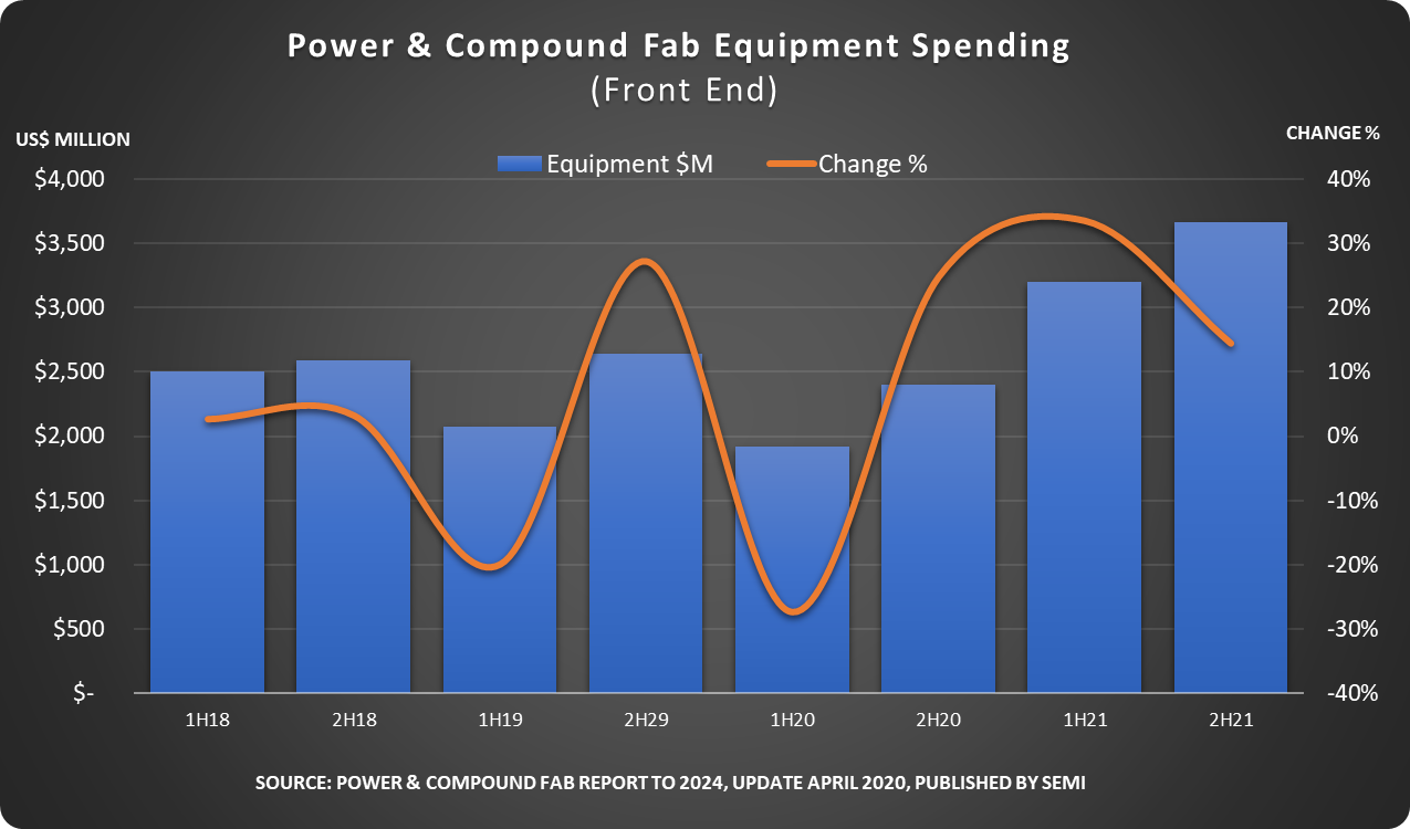
In breakdowns by region, China will expand power and compound fab capacity by 50 percent and 87 percent, respectively, from 2019-2024, more than any other region. Over the same period, Europe/Mideast and Taiwan will lead the way in adding power fab capacity, while the Americas and Europe/Mideast will be among those regions adding compound fab capacity.
For more information about The SEMI Power & Compound Fab Report to 2024 or to download sample data from the report, please click here.
About SEMI
SEMI® connects more than 2,100 member companies and 1.3 million professionals worldwide to advance the technology and business of electronics design and manufacturing. SEMI members are responsible for the innovations in materials, design, equipment, software, devices, and services that enable smarter, faster, more powerful, and more affordable electronic products. Electronic System Design Alliance (ESD Alliance), FlexTech, the Fab Owners Alliance (FOA) and the MEMS & Sensors Industry Group (MSIG) are SEMI Strategic Association Partners, defined communities within SEMI focused on specific technologies. Visit www.semi.org to learn more, contact one of our worldwide offices, and connect with SEMI on LinkedIn and Twitter.
Association Contact
Michael Hall/SEMI
Phone: 1.408.943.7988
Email: [email protected]


MILPITAS, Calif. — May 4, 2020 — Worldwide silicon wafer area shipments rose 2.7 percent to 2,920 million square inches in the first quarter of 2020, compared with fourth-quarter 2019 shipments of 2,844 million square inches, but dropped 4.3 percent year-over-year, the SEMI Silicon Manufacturers Group (SMG) reported in its quarterly analysis of the silicon wafer industry.

"Global silicon wafer shipments rebounded slightly in the first quarter of 2020 after declining for one year,” said Neil Weaver, chairman SEMI SMG and vice president, Product Development and Applications Engineering at Shin Etsu Handotai America. “However, with the disruptions caused by the coronavirus, market uncertainty will prevail in the upcoming quarters.”
Silicon Area Shipment Trends – Semiconductor Applications Only
|
Millions of Square Inches |
||||||
|
|
4Q 2018 |
1Q 2019 |
2Q 2019 |
3Q 2019 |
4Q 2019 |
1Q 2020 |
|
Total |
3,234 |
3,051 |
2,983 |
2,932 |
2,844 |
2,920 |
Source: SEMI (www.semi.org), April 2020
All data cited in this release includes polished silicon wafers such as virgin test wafers and epitaxial silicon wafers, as well as non-polished silicon wafers shipped to end users.
Silicon wafers are the fundamental building material for semiconductors, which, in turn, are vital components of virtually all electronics goods, including computers, telecommunications products and consumer electronics. The highly engineered thin, round disks are produced in various diameters – from one inch to 12 inches – and serve as the substrate material on which most semiconductor devices, or chips, are fabricated.
A sub-committee of the SEMI Electronic Materials Group (EMG), the SMG is open to SEMI members involved in manufacturing polycrystalline silicon, monocrystalline silicon or silicon wafers (e.g., as cut, polished, epi). The purpose of the SMG is to facilitate collective efforts on issues related to the silicon industry including the development of market information and statistics about the silicon industry and the semiconductor market.
For more information, please visit SEMI Worldwide Silicon Wafer Shipment Statistics.
About SEMI
SEMI® connects more than 2,260 member companies and 1.3 million professionals worldwide to advance the technology and business of electronics manufacturing. SEMI members are responsible for the innovations in materials, design, equipment, software, devices, and services that enable smarter, faster, more powerful, and more affordable electronic products. Electronic System Design Alliance (ESD Alliance), FlexTech, the Fab Owners Alliance (FOA) and the MEMS & Sensors Industry Group (MSIG) are SEMI Strategic Association Partners, defined communities within SEMI focused on specific technologies. Visit www.semi.org to learn more, contact one of our worldwide offices, and connect with SEMI on LinkedIn and Twitter.
Association Contact
Michael Hall/SEMI
Phone: 1.408.943.7988
Email: [email protected]


MILPITAS, Calif. — April 23, 2020 — North America-based manufacturers of semiconductor equipment posted $2.21 billion in billings worldwide in March 2020 (three-month average basis), according to the March Equipment Market Data Subscription (EMDS) Billings Report published today by SEMI. The billings figure is 6.8 percent lower than the final February 2020 level of $2.37 billion, and is 21.2 percent higher than the March 2019 billings level of $1.83 billion.
“While March monthly billings of North America-based semiconductor equipment manufacturers are starting to reflect a challenging market environment, the year-over-year increase indicates companies across the semiconductor manufacturing supply chain thus far are effectively maintaining continuous operations despite COVID-19 headwinds,” said Ajit Manocha, SEMI president and CEO.
The SEMI Billings report uses three-month moving averages of worldwide billings for North American-based semiconductor equipment manufacturers. Billings figures are in millions of U.S. dollars.
|
|
Billings |
Year-Over-Year |
|
October 2019 |
$2,080.8 |
2.5% |
|
November 2019 |
$2,121.0 |
9.1% |
|
December 2019 |
$2,491.7 |
18.4% |
|
January 2020 |
$2,340.2 |
23.4% |
|
February 2020 (final) |
$2,374.6 |
27.1% |
|
March 2020 (prelim) |
$2,213.1 |
21.2% |
Source: SEMI (www.semi.org), April 2020
SEMI publishes a monthly North American Billings report and issues the Worldwide Semiconductor Equipment Market Statistics (WWSEMS) report in collaboration with the Semiconductor Equipment Association of Japan (SEAJ). The WWSEMS report currently reports billings by 24 equipment segments and by seven end market regions. SEMI also has a long history of tracking semiconductor industry fab investments in detail on a company-by-company and fab-by-fab basis in its World Fab Forecast and SEMI FabView databases. These powerful tools provide access to spending forecasts, capacity ramp, technology transitions, and other information for over 1,000 fabs worldwide. For an overview of available SEMI market data, please visit www.semi.org/en/MarketInfo.
The data contained in this release were compiled by David Powell, Inc., an independent financial services firm, without audit, from data submitted directly by the participants. SEMI and David Powell, Inc. assume no responsibility for the accuracy of the underlying data.
About SEMI
SEMI® connects more than 2,100 member companies and 1.3 million professionals worldwide to advance the technology and business of electronics design and manufacturing. SEMI members are responsible for the innovations in materials, design, equipment, software, devices, and services that enable smarter, faster, more powerful, and more affordable electronic products. Electronic System Design Alliance (ESD Alliance), FlexTech, the Fab Owners Alliance (FOA) and the MEMS & Sensors Industry Group (MSIG) are SEMI Strategic Association Partners, defined communities within SEMI focused on specific technologies. Visit www.semi.org to learn more, contact one of our worldwide offices, and connect with SEMI on LinkedIn and Twitter.
Association Contact
Michael Hall/SEMI
Phone: 1.408.943.7988
Email: [email protected]
Notes
Next SEMI Billings report is May 21, 2020 at 3:00pm Pacific.
For information on SEAJ Billings Express Report, visit www.seaj.or.jp.