downloadGroupGroupnoun_press release_995423_000000 copyGroupnoun_Feed_96767_000000Group 19noun_pictures_1817522_000000Member company iconResource item iconStore item iconGroup 19Group 19noun_Photo_2085192_000000 Copynoun_presentation_2096081_000000Group 19Group Copy 7noun_webinar_692730_000000Path
Skip to main content
Default Banner Image

SEMI Press Release

ID
semi-press-release

【July 3, 2025 – Hsinchu】As demand for AI and HPC accelerates, the semiconductor industry is embracing a new era. With Moore’s Law slowing and scaling challenges rising, technologies like 3DIC, Fan-Out Panel Level Packaging (FOPLP), chiplets, and co-packaged optics (CPO) are becoming essential for next-level performance and system integration. SEMICON Taiwan 2025 will spotlight these advances through global forums starting September 8, ahead of the main exhibition from September 10–12 at Taipei Nangang Exhibition Center.


Explosive Growth in Advanced Packaging Market Redefines Industry Value Chain

“Fueled by soaring AI demand, advanced manufacturing capacity is expected to hit a record 1.4 million wafers per month by 2028,” said Terry Tsao, Global Chief Marketing Officer and President of Taiwan, SEMI. “As AI demands surpass the limits of single-chip scaling, advanced packaging technologies like 3DIC and FOPLP are essential for system-level integration. With the industry moving from a linear supply chain to a more integrated and collaborative ecosystem, SEMICON Taiwan 2025 will serve as a vital global platform for industry leaders to explore how packaging and manufacturing innovation can unlock new commercial value across the semiconductor landscape.”
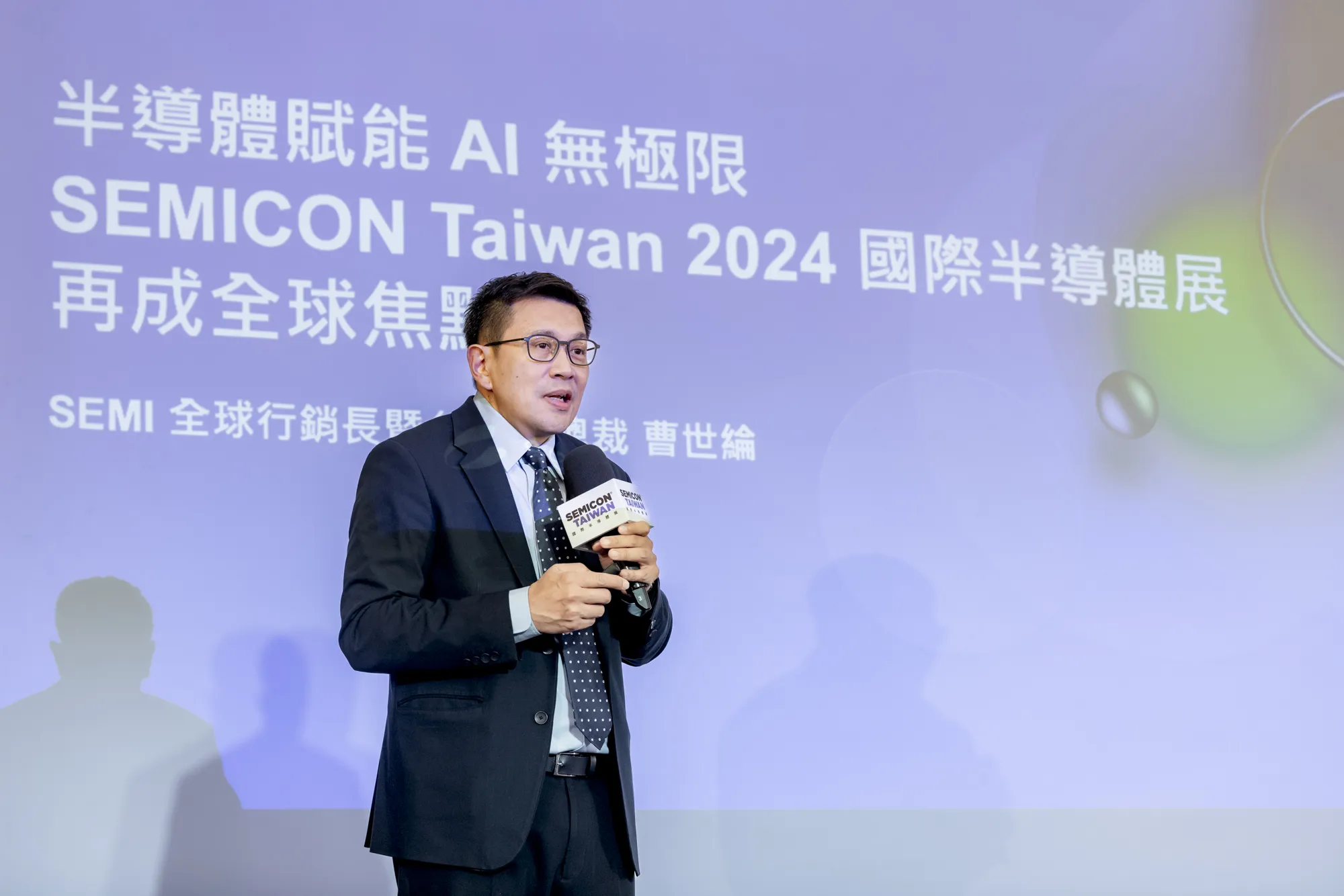
 

SEMI全球行銷長暨台灣區總裁曹世綸表示,3DIC、FOPLP等先進封裝技術正成為實現系統級整合的關鍵路徑。

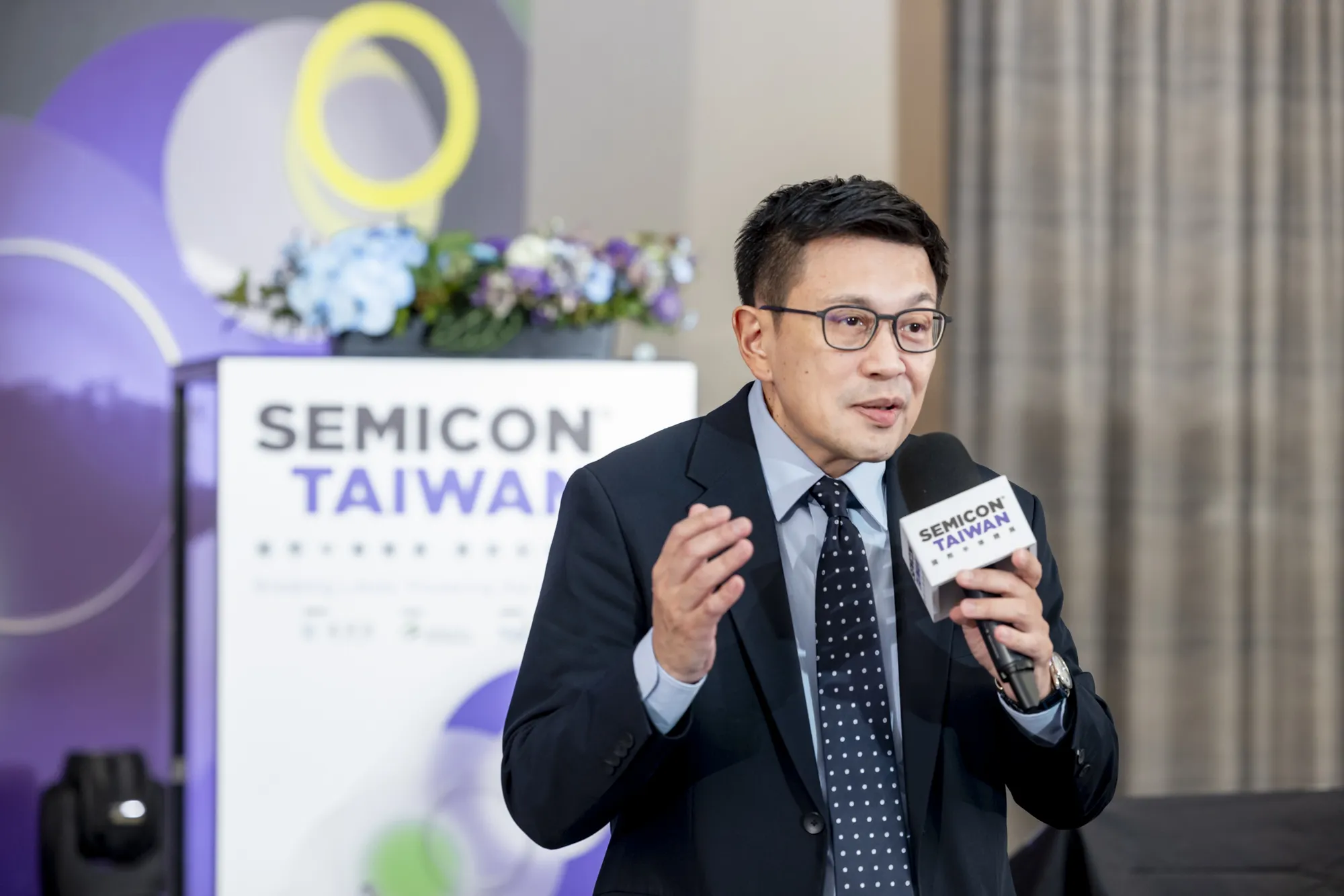
▲Terry Tsao, Global Chief Marketing Officer and President of Taiwan, SEMI


SEMI Promotes Global Collaborative Platform – 3DIC Advanced Manufacturing Alliance

As global supply chains are restructuring and geopolitical tensions rise, Asia is accelerating advanced packaging innovation, with Taiwan emerging as a strategic hub. To drive global collaboration and next-gen system integration, SEMI will officially launch the highly anticipated 3DIC Advanced Manufacturing Alliance (3DICAMA) at SEMICON Taiwan 2025. The alliance marks a key shift from single-chip to system-level solutions, aiming to boost cross-industry collaboration, enhance supply chain resilience, promote standards adoption, and speed up technology commercialization, laying the groundwork for a highly integrated and efficient packaging ecosystem.


World’s Top Advanced Packaging Platform at SEMICON Taiwan 2025

SEMICON Taiwan 2025 will host the Heterogeneous Integration Global Summit (HIGS), FOPLP Innovation Forum, and 3DIC Global Summit, covering critical topics from design and materials to process and supply chain. These high-level forums will map the future of advanced packaging and integration technologies. Industry leaders, including ASE, Broadcom, Lightmatter, MediaTek, Nvidia, Sony, and TSMC, will join HIGS Series to tackle challenges in 3DIC, CPO, and AI packaging. At the FOPLP Innovation Forum, AMD and PTI experts will share the latest innovations and market applications strategies.

 

SEMICON Taiwan 2025將串聯異質整合國際高峰論壇 (HIGS)、FOPLP 創新論壇與3DIC 全球高峰論壇,聚焦設計、材料、製程至供應鏈的全方位議題,勾勒先進封裝與異質整合技術的發展藍圖。

▲SEMICON Taiwan 2025 to Present the World's Most Comprehensive Advanced Packaging Technology Platform


This year’s Heterogeneous Integration Area will expand to three pavilions: 3DIC Advanced Packaging, FOPLP, and Semiconductor Packaging, featuring cutting-edge technologies, tech demonstrations, industry standards, and supply chain collaboration. Leading companies such as Innolux, PTI, Comet, Coherent, E&R Engineering, GP, Lam Research, Manz, Mirle, PDF Solutions, PSK, Shibaura, and Utechzone will showcase state-of-the-art system-level solutions and integration applications, offering attendees key insights and partnership opportunities.


Registration for SEMICON Taiwan 2025 is now open. Apply for FREE visitor codes by August 31 and receive 30% off the International Semiconductor Forum with limited-time early bird rates. Visit the Official website.


About SEMI

SEMI® is the global industry association connecting over 3,000 member companies and 1.5 million professionals worldwide across the semiconductor and electronics design and manufacturing supply chain. We accelerate member collaboration on solutions to top industry challenges through Advocacy, Workforce Development, Sustainability, Supply Chain Management, and other programs. Our SEMICON® expositions and events, technology communities, standards, and market intelligence help advance our members’ business growth and innovations in design, devices, equipment, materials, services, and software, enabling smarter, faster, more secure electronics. Visit  www.semi.org  or join SEMI Facebook, and SEMI LinkedIn, and SEMI Official Line Account.
 

MILPITAS, Calif. – July 7, 2025 – SEMI, the global industry association advancing the electronics manufacturing and design supply chain, today launched the new Wafer Fab Materials Quarterly report in collaboration with Linx Consulting. SEMI recently acquired select assets from Linx Consulting, including market reports and conferences, to amplify its market intelligence capabilities in semiconductor materials and specialty chemicals.

SEMI & LINXThe Wafer Fab Materials Quarterly is a comprehensive report delivering in-depth analysis and forecasts for global wafer fab materials markets. Published quarterly in January, April, July, and October, it equips industry professionals with actionable insights into economic trends, material usage, sales performance, and capacity forecasts. This collaborative effort harnesses SEMI’s extensive industry data and Linx Consulting’s analytical and forecasting expertise to support strategic and operational decision-making.
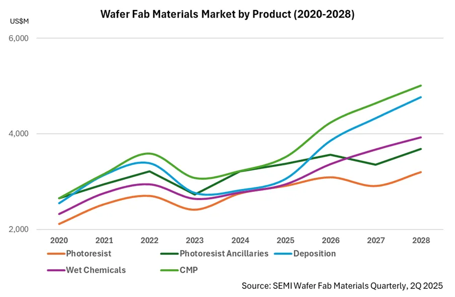

“The launch of this new quarterly materials report complements our market intelligence portfolio, offering deeper insights into the increasingly important materials market,” said Clark Tseng, Senior Director of Market Intelligence at SEMI. “By delivering detailed, forward-looking data every quarter, the Wafer Fab Materials Quarterly helps industry leaders to quickly respond to market shifts and make more informed decisions than annual reports allow.”

Report highlights:

  • Comprehensive Market Coverage: Segmented forecasts for silicon wafers, photoresists, gases, deposition materials, wet chemicals, and CMP materials, with breakdowns by product segment and end-use application.
  • Quarterly Performance Tracking: Exclusive sales data for leading suppliers and semiconductor companies, enabling benchmarking and market share analysis.
  • Capacity and Materials Intensity: Capacity forecasts by product type, region, and wafer size, plus cost-per-wafer insights by process node.
  • Macroeconomic Context: Global indicators like GDP, industrial production, and CPI to frame semiconductor market trends.
  • Industry Overview: Analysis of semiconductor sales, CapEx, silicon MSI, inventory, and utilization rates.

The inaugural 2Q 2025 edition reveals a dynamic transformation in wafer fab materials markets, with the industry demonstrating remarkable resilience through its recovery trajectory. Following the 2023 materials downturn, the sector achieved robust growth in 2024, led by photoresist materials surging 14% after an 11% contraction the previous year. 

The report highlights how technology evolution is driving unprecedented demand for advanced materials, with advanced photoresist now representing over 80% of market revenue and projected to reach 84% by 2028. Chemical mechanical planarization (CMP) materials emerge as the standout growth segment, benefiting significantly from increasing device complexity and layer counts in next-generation semiconductors. With advanced process nodes (≤7nm) capacity growing at a 20% CAGR through 2028, there is increasing demand for innovative material solutions that support atomic-scale precision manufacturing. 

WFM

Delivered in Microsoft Excel and PowerPoint formats, the SEMI Wafer Fab Materials Quarterly report offers historical data from 2020 and forecasts through 2028, allowing users to manipulate data, integrate it into business models, and perform custom analyses. The report supports strategic planning, operational optimization, and technology innovation across the supply chain.

For details about SEMI reports on other semiconductor sectors, visit SEMI Market Data or contact the SEMI Market Intelligence team at [email protected].

About SEMI

SEMI® is the global industry association connecting over 3,000 member companies and 1.5 million professionals worldwide across the semiconductor and electronics design and manufacturing supply chain. We accelerate member collaboration on solutions to top industry challenges through Advocacy, Workforce Development, Sustainability, Supply Chain Management and other programs. Our SEMICON® expositions and events, technology communities, standards and market intelligence help advance our members’ business growth and innovations in design, devices, equipment, materials, services and software, enabling smarter, faster, more secure electronics. Visit www.semi.org, contact a regional office, and connect with SEMI on LinkedIn and X to learn more.

About Linx Consulting

Linx Consulting is a leading provider of market intelligence and consulting services to the semiconductor and electronics industries. Known for its in-depth market reports and high-caliber conferences, Linx Consulting has been a trusted partner to industry leaders for over two decades.

Association Contact

Sherrie Gutierrez/SEMI
Phone: 1.831.889.3800 
Email: [email protected]

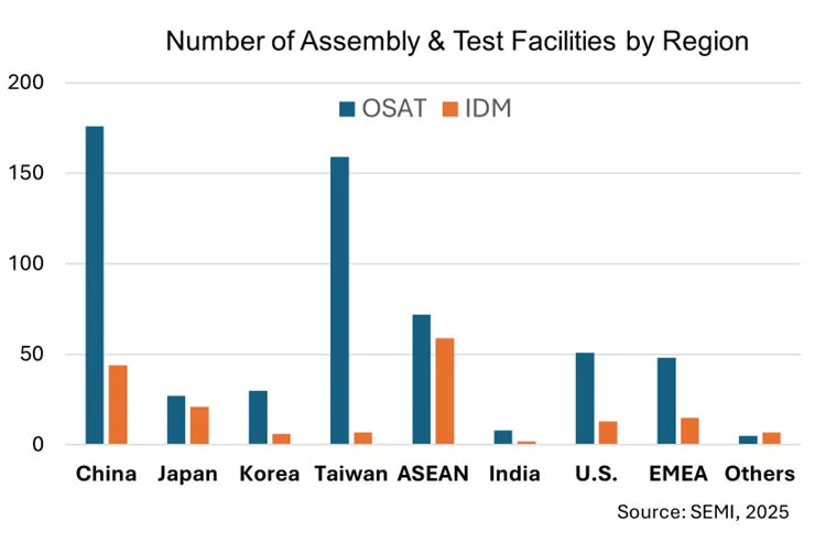
MILPITAS, Calif. – July 1, 2025 – SEMI and TechSearch International today announced the release of the 2025 edition of the Worldwide Semiconductor Assembly & Test Facility Database, the industry’s most comprehensive resource tracking global assembly and test sites operated by integrated device manufacturers (IDMs) and outsourced semiconductor assembly and test providers (OSATs).

The Worldwide Assembly & Test Facility Database remains an indispensable tool for mapping the global semiconductor supply chain, identifying new capacity, and tracking technology adoption across regions. The 2025 report’s expanded content and improved structure further strengthen its value for industry stakeholders seeking actionable intelligence in a rapidly evolving market.

“The 2025 edition of the Worldwide Assembly & Test Facility Database reflects the dynamic growth and increasing complexity of the global semiconductor supply chain,” said Clark Tseng, Senior Director of Market Intelligence at SEMI. “By expanding our coverage and incorporating new data features, we are providing industry stakeholders with a deeper understanding of global packaging and testing capabilities, technology adoption, and regional trends as the market continues to evolve.”

The 2025 edition delivers several significant updates and enhancements:

  • Expanded Coverage: The database now includes 750 facilities worldwide, an increase of 70 new sites compared to the 2024 edition, reflecting ongoing industry investment and expansion.
  • Enhanced Data Structure: New columns have been added to improve data granularity and usability:
    • Each facility is now assigned a unique Facility ID for easier reference and tracking.
    • Additional columns detail device types, including memories, logic/analog ICs, power devices, RF/MEMS chips, and CMOS image sensors, enabling users to identify specialized manufacturing and test capabilities at a glance.
    • The startup year for some facilities is now included, providing insights into the operational history and maturity of each site.
  • Regular Facility Updates: In addition to these new features, the database continues to offer up-to-date information on facility status, ownership, location, plant type, production capabilities, and certification status, supporting strategic decision-making for manufacturers, suppliers, and analysts.
Number of assembly & test facilities

For details about SEMI reports on other semiconductor sectors, visit SEMI Market Data or contact the SEMI Market Intelligence team at [email protected].

About SEMI

SEMI® is the global industry association connecting over 3,000 member companies and 1.5 million professionals worldwide across the semiconductor and electronics design and manufacturing supply chain. We accelerate member collaboration on solutions to top industry challenges through Advocacy, Workforce Development, Sustainability, Supply Chain Management and other programs. Our SEMICON® expositions and events, technology communities, standards and market intelligence help advance our members’ business growth and innovations in design, devices, equipment, materials, services and software, enabling smarter, faster, more secure electronics. Visit www.semi.org, contact a regional office, and connect with SEMI on LinkedIn and X to learn more.

Association Contact

Sherrie Gutierrez/SEMI
Phone: 1.831.889.3800 
Email: [email protected]

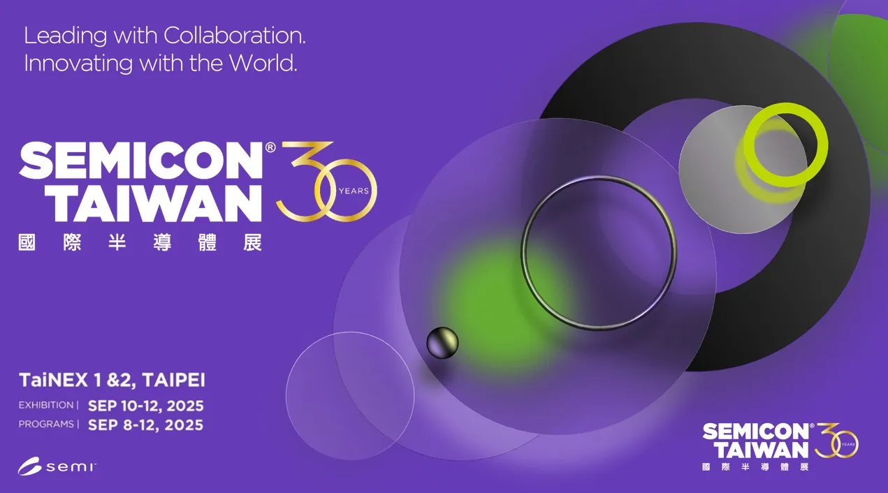
MILPITAS, Calif. – July 8, 2025 – SEMI today announced its 30th annual SEMICON Taiwan event – the premier conference and exhibition for the global semiconductor industry. SEMICON Taiwan 2025 will begin with a series of forums from September 8-9 at the Taipei Nangang Exhibition Center, with the primary exhibition taking place from September 10-12. Themed Leading with Collaboration. Innovating with the World, SEMICON Taiwan will facilitate global industry partnerships and help power the next wave of technological transformation. Registration is open.

SEMICON Taiwan“Global semiconductor equipment shipments hit $32.05 billion USD in Q1 2025, up 21% YoY, driven by strong demand for AI, cloud, high-performance computing, and edge applications,” said Terry Tsao, Global Chief Marketing Officer and President of Taiwan, SEMI. “However, despite robust growth, supply chain and geopolitical challenges remain. As a crucial global semiconductor hub, Taiwan is fully committed to pushing forward with new technologies and standards. SEMICON Taiwan’s theme reflects our drive to foster innovation and strengthen global partnerships to build a resilient and highly connected industry ecosystem.”

SEMICON Taiwan 2025 Highlights and Attractions

Expected Record Attendance

  • SEMICON Taiwan 2025 is on track to break its annual attendance records. With over 100,000 visitors and more than 1,100 companies and industry partners from 56 countries expected to register for the event, attendees will come together to explore the latest semiconductor industry trends, exchange technical knowledge, and foster cross-border collaboration. A record 17 Country Pavilions will provide additional opportunities for industry dialogue and partnerships.

Cutting-Edge Technologies 

Focus on Geostrategy, Talent Development, and Sustainability

  • In response to global supply chain restructuring and geopolitical challenges, this year’s forum will include dedicated sessions that will address supply chain resilience and foster global collaboration. In addition, SEMICON Taiwan will feature SEMI’s signature Workforce Development Pavilion, as well as a 20 Under 40 & Tech Master Forum and hands-on activities to inspire future industry talent.
  • SEMI Taiwan will also include an expanded Green Manufacturing Area to showcase best practices in green manufacturing. This year’s Green Manufacturing Area will include dedicated pavilions for reclaimed water, decarbonization, air pollution control, energy management, and more. 

Industry professionals can apply for free visitor discount codes through August 31. For more details, visit the SEMICON Taiwan website or view the full conference agenda.

About SEMI

SEMI® is the global industry association connecting over 3,000 member companies and 1.5 million professionals worldwide across the semiconductor and electronics design and manufacturing supply chain. We accelerate member collaboration on solutions to top industry challenges through Advocacy, Workforce Development, Sustainability, Supply Chain Management, and other programs. Our SEMICON® expositions and events, technology communities, standards, and market intelligence help advance our members’ business growth and innovations in design, devices, equipment, materials, services, and software, enabling smarter, faster, more secure electronics. Visit www.semi.org, contact a regional office, and connect with SEMI on LinkedIn and X to learn more.

Association Contacts

Sherrie Gutierrez / SEMI Corporate
Phone: 1.831.889.3800 
Email: [email protected]

Peyton Sun / SEMI 
Phone: 03-560-1777 #209
Email: [email protected]

Roselie Chen / Golin
Phone: 0984-349-379
Email: [email protected]

Alice Lin / Golin
Phone: 0919-552-589
Email: [email protected]

BRUSSELS, Belgium – June 30, 2025 – SEMI, the industry association serving the global electronics design and manufacturing supply chain, today released its official position paper on the revision of the European Union’s REACH Regulation. The paper outlines the semiconductor industry’s priorities for ensuring that the revised regulation supports sustainable manufacturing in Europe while protecting the technological resilience and competitiveness of Europe’s semiconductor industry.

“Semiconductors are at the core of Europe’s green and digital transition, and the REACH revision must reflect the unique role our industry plays in enabling this future,” said Laith Altimime, President of SEMI Europe. “This paper highlights how a more tailored, risk-based approach to regulation can ensure continued access to critical materials, foster innovation, and uphold the EU’s leadership in sustainable manufacturing.”

The REACH revision proposal is expected in Q4 2025. With key regulatory decisions approaching, SEMI Europe is calling for a balanced and forward-looking framework that enables both environmental protection and technological progress.

Key recommendations from SEMI Europe include:

  • Introducing sector-specific derogations and realistic transition timelines for complex industrial sectors such as semiconductors.
  • Ensuring restriction decisions are based on full risk assessments that account for real-world use and exposure, rather than hazard alone.
  • Avoiding mandatory polymer registration for proprietary process chemicals already governed under existing frameworks.
  • Applying substance grouping and substitution planning with greater scientific precision, especially for critical-use substances.
  • Clarifying and operationalizing the essential use concept in a transparent, proportionate, and industry-relevant manner.
  • Strengthening nanomaterials regulation through targeted updates to safety data sheets, testing guidelines, and integration of the revised EU definition.

The paper also highlights the importance of ensuring that the REACH revision does not conflict with strategic EU initiatives, including the European Chips Act, and calls for deeper engagement between regulators and high-technology industries in shaping effective, innovation-compatible policy.

“SEMI Europe stands ready to work with EU institutions, regulators, and relevant stakeholders to ensure the REACH revision reflects both scientific evidence and the operational realities of the semiconductor sector,” said Altimime. “By aligning regulatory ambition with industrial capabilities, Europe can achieve its sustainability goals while preserving long-term strategic resilience.”

Read the full position paper.

SEMI Europe Advocacy

Discover how SEMI Europe Advocacy & Public Policy supports the microelectronics industry across sustainability, trade, talent, and R&D—or become involved by contacting [email protected]. 

About SEMI

SEMI® is the global industry association connecting over 3,000 member companies and 1.5 million professionals worldwide across the semiconductor and electronics design and manufacturing supply chain. We accelerate member collaboration on solutions to top industry challenges through Advocacy, Workforce Development, Sustainability, Supply Chain Management, and other programs. Our SEMICON® expositions and events, technology communities, standards, and market intelligence help advance our members’ business growth and innovations in design, devices, equipment, materials, services, and software, enabling smarter, faster, more secure electronics. Visit www.semi.org, contact a regional office, and connect with SEMI on LinkedIn and X to learn more.

Contact Information:

Iranda Chaki / SEMI Europe
Email: [email protected] 

Samer Bahou / SEMI Corporate
Phone: +1 408 943 7870
Email: [email protected]

DRESDEN, Germany — June 24, 2025 — More than 150 global experts are set to convene in Dresden from June 25–27 for the SEMI 3D & Systems Summit 2025 to explore the latest breakthroughs in 3D packaging and heterogeneous integration. Registration is open. 

Themed Heterogeneous Integration: Bolstering Europe’s Resilience, the summit will explore innovations in chiplet architectures, die-to-wafer and wafer-to-wafer hybrid bonding, photonics, and advanced system-level design. From geopolitical dynamics and advanced packaging breakthroughs to high-performance computing and biomedical applications, the program will offer insights into how 3D and heterogeneous integration technologies are reshaping Europe’s semiconductor value chain.

3D systems & summit “The SEMI 3D & Systems Summit opens here in Dresden tomorrow to welcome industry leaders, technology innovators, and future talent to exchange ideas and advance collaboration on technologies critical to Europe’s semiconductor future,” said Laith Altimime, President of SEMI Europe. “This year’s focus on heterogeneous integration reflects our shared commitment to strengthening Europe’s resilience and global competitiveness through innovation, and to investing in the next generation of semiconductor professionals who will drive this transformation.”
A key highlight of this year’s Summit is the NextGen Talent session, designed to connect students and young professionals with industry leaders as Europe works to build a strong pipeline of semiconductor talent. This dedicated session will explore how collaboration between academia and industry can help close critical skill gaps and foster innovation. Program highlights include A Day in the Life talks, providing students with first-hand insights into semiconductor careers, and the panel discussion What Fab Managers Want: Talent, Workforce, and HR Perspectives. Additional activities, including a Student Quiz and Flash Mentoring session, will offer valuable opportunities for emerging talent to engage with experienced professionals and explore meaningful career pathways within the industry.

Participating Mentors

Featured Speakers 

Global Leaders to Present  

3D & Systems Summit presenters include experts from global leaders:  

  • AEMtec GmbH

  • Adeia

  • ASML

  • ASE Group

  • Atotech (MKS)

  • BESI

  • Bosch Semiconductor Manufacturing Dresden

  • CEA-Leti

  • Chipletz

  • Comet

  • Confovis

  • Dresden Chip Academy (SBH Nordost GmbH)

  • EV Group

  • Evatec

  • European Semiconductor Manufacturing Company (ESMC)

  • Fraunhofer Group for Microelectronics

  • Fraunhofer IZM-ASSID 

  • HEIDENHAIN GmbH

  • imec

  • Infineon Technologies GmbH & Co KG

  • Infinitesima

  • Intel

  • KLA

  • Lam Research

  • NXP Semiconductors

  • SET (Smart Equipment Technology)

  • Soitec

  • SPTS Technologies

  • SUSS MicroTec

  • Syenta

  • TechSearch International, Inc.

  • TU Dresden

  • Yole Group

Exhibition and Networking  

The most prominent names in 3D integration microelectronics manufacturing will showcase their latest products and technologies in the new exhibition area. Exhibitors include: AEMtec GmbH, Adeia Inc., ASE Global, ASMPT, Besi, Carl Zeiss (ZEISS Microscopy), Comet, Confovis, cyberTECHNOLOGIES, DISCO HI-TEC Europe, FAMES, Fraunhofer IZM-ASSID, Fraunhofer - Verbund Mikroelektronik (FMD), Heidenhain, Kistler AG, Kontron AIS, NanoFocus AG, PLANOPTIK, Precitec Optronik GmbH, SET (Smart Equipment Technology), Syenta, Wooptix.

This year’s networking reception will take place at the Hilton Dresden Hotel on the first day of the event, and the Networking Dinner Cruise is set on a historic paddle steamer on the Elbe River.

3D Summit Premium Sponsors: 

For more details, please visit the 3D & Systems Summit 2025 website and connect with SEMI Europe on LinkedIn or YouTube @SEMIEurope (#3DSummit).  


About SEMI 

SEMI® is the global industry association connecting over 3,000 member companies and 1.5 million professionals worldwide across the semiconductor and electronics design and manufacturing supply chain. We accelerate member collaboration on solutions to top industry challenges through Advocacy, Workforce Development, Sustainability, Supply Chain Management and other programs. Our SEMICON® expositions and events, technology communities, standards and market intelligence help advance our members’ business growth and innovations in design, devices, equipment, materials, services and software, enabling smarter, faster, more secure electronics. Visit www.semi.org, contact a regional office, and connect with SEMI on LinkedIn and X to learn more.  

Contact Information: 

Sitong He / SEMI Europe  
Phone: +49 151 55462638
Email: [email protected]   

Sherrie Gutierrez / SEMI Corporate 
Phone: +1 831 889 3800  
Email: [email protected] 

MILPITAS, Calif. – June 25, 2025 – SEMI, the industry association serving the global semiconductor and electronics design and manufacturing supply chain, today reported findings from its latest 300mm Fab Outlook report. The report shows global front-end semiconductor suppliers are accelerating expansion efforts to support the surging demand for generative AI applications. 

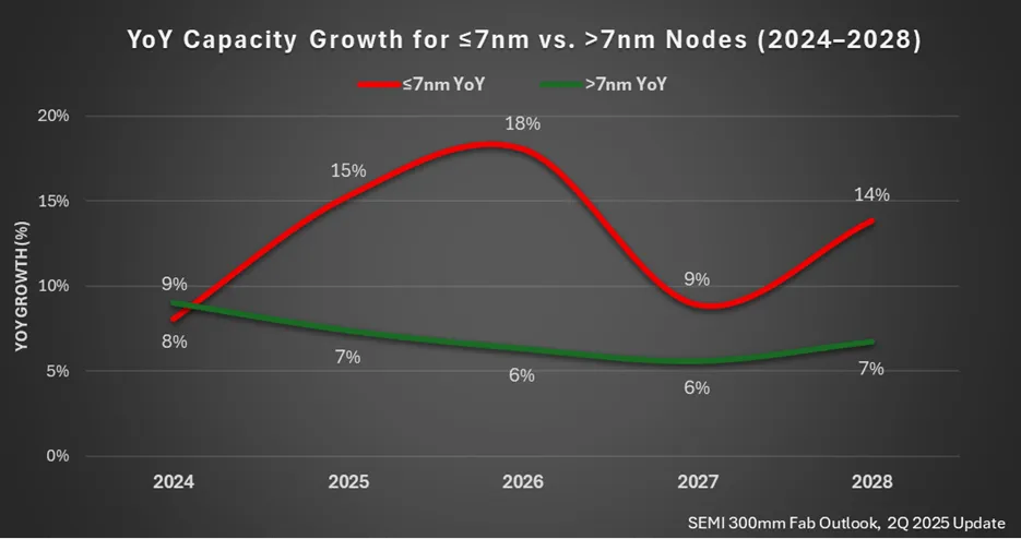
According to the 300mm Fab Outlook report, the global semiconductor manufacturing industry is expected to maintain strong momentum, with capacity projected to grow at a compound annual growth rate (CAGR) of 7% from the end of 2024 through 2028, reaching a record high of 11.1 million wafers per month (wpm).

A key driver of this growth is the continued expansion of advanced process capacity (7nm and below), which is expected to increase by approximately 69% – from 850,000 wpm in 2024 to a historic high of 1.4 million wpm in 2028 – representing a CAGR of around 14%, double the industry average.

“AI continues to be a transformative force in the global semiconductor industry, driving significant expansion of advanced manufacturing capacity,” said SEMI President and CEO Ajit Manocha. “The rapid proliferation of AI applications is stimulating robust investment across the semiconductor ecosystem, underscoring the industry’s pivotal role in fostering technology innovation and meeting the surging demand for advanced chips.”

YoY


AI Continues to Drive Demand for Advanced Nodes

Beyond the demand for increasingly powerful training capabilities to support larger AI model architectures, AI inference has emerged as another critical catalyst for growth. Market expansion is further fueled by AI’s integration into system software for personal assistants and innovative applications.

Moreover, AI is also enabling new breakthroughs in virtual and augmented reality devices, as well as humanoid robotic sectors, which are expected to sustain strong demand for advanced semiconductor technologies over the next several years.

Advanced Process Capacity Expansion Maintains Double-Digit Growth

Advanced process capacity is projected to maintain a robust 14% CAGR from 2025 through 2028, beginning with 982 thousand wpm in 2025, representing 15% YoY growth. The industry is expected to achieve a significant milestone in 2026, surpassing one million wafers for the first time, with capacity reaching 1.16 million wpm.

2nm and below capacity deployment shows even more aggressive scaling throughout the forecast period, with production capacity expanding dramatically from less than 200 thousand wpm in 2025 to over 500 thousand wpm by 2028, reflecting the strong market demand driven by AI applications in advanced manufacturing.

Fab Equipment in Advanced Technology Soar in 2025 and 2027

The semiconductor industry’s investment landscape remains firmly anchored in advanced process technologies. Capital expenditure on advanced process equipment is forecast to surge to over US$50 billion by 2028, representing a substantial 94% increase from the US$26 billion invested in 2024. This trajectory underscores the industry’s resolute commitment to next-generation manufacturing capabilities, reflecting a robust 18% CAGR.

The transition to cutting-edge nodes continues to accelerate, with 2nm technology projected to reach mass production by 2026, followed by the commercial deployment of 1.4 nm technology in 2028. In anticipation of growing market demand, chip manufacturers are strategically expanding production capacity ahead of schedule, with growth rates of 33% in 2025 and 21% in 2027, respectively.

Investment in 2nm and below wafer equipment represents a particularly dramatic expansion, with funding more than doubling from US$19 billion in 2024 to US$43 billion in 2028. A remarkable 120% increase that underscores the industry’s aggressive pursuit of next-generation manufacturing capabilities.

Download a sample of the SEMI 300mm Fab Outlook.

For more information about the report or to subscribe, please contact the SEMI Market Intelligence Team at [email protected]. More details are also available on the SEMI Market Data webpage.  

About SEMI

SEMI® is the global industry association connecting over 3,000 member companies and 1.5 million professionals worldwide across the semiconductor and electronics design and manufacturing supply chain. We accelerate member collaboration on solutions to top industry challenges through Advocacy, Workforce Development, Sustainability, Supply Chain Management and other programs. Our SEMICON® expositions and events, technology communities, standards and market intelligence help advance our members’ business growth and innovations in design, devices, equipment, materials, services and software, enabling smarter, faster, more secure electronics. Visit www.semi.org, contact a regional office, and connect with SEMI on LinkedIn and X to learn more.

Association Contacts

Sherrie Gutierrez/SEMI
Phone: 1.831.889.3800 
Email: [email protected]

Christian G. Dieseldorff/SEMI US
Phone: 1.408.943.7940
Email: [email protected]    

Chih-Wen Liu/SEMI Taiwan
Phone: 886.3.560.1777
Email: [email protected]

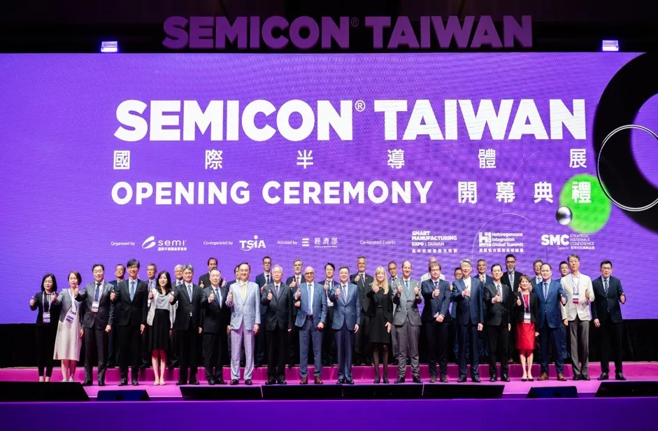
【June 18, 2025 – Hsinchu】SEMI today officially announced the launch of SEMICON Taiwan 2025, the annual premier event for the global semiconductor industry. Marking its 30th anniversary, the exhibition spotlights Taiwan’s rise as a collaborative innovation powerhouse. This year’s edition kicks off with a series of summit forums starting September 8, with the main exhibition officially opening from September 10 - 12 at Taipei Nangang Exhibition Center. Under the theme Leading with Collaboration. Innovating with the World, SEMICON Taiwan will strengthen global ecosystem partnerships and power the next wave of industry innovation.


Growth Amid Challenges: Open Collaboration Defines the New Industry Paradigm

“Global semiconductor equipment shipments hit US$32.05 billion in Q1 2025, up 21% YoY, driven by strong demand for AI, cloud, HPC, and edge applications*,” said Terry Tsao, Global Chief Marketing Officer and President of Taiwan, SEMI. “Even with this robust growth, supply chain and geopolitical challenges remain. As a crucial global semiconductor hub, Taiwan is fully committed to pushing forward with new technologies and standards. Our theme, Leading with Collaboration. Innovating with the World. reflects our drive to foster innovation and strengthen global partnerships. SEMI will continue to work with partners to build a resilient and highly connected ecosystem.”


SEMICON Taiwan 2025 Marks Official Launch

▲SEMICON Taiwan 2025 Marks Official Launch

Terry Tsao, Global Chief Marketing Officer and President of Taiwan, SEMI

▲Terry Tsao, Global Chief Marketing Officer and President of Taiwan, SEMI


Highlights of SEMICON Taiwan 2025

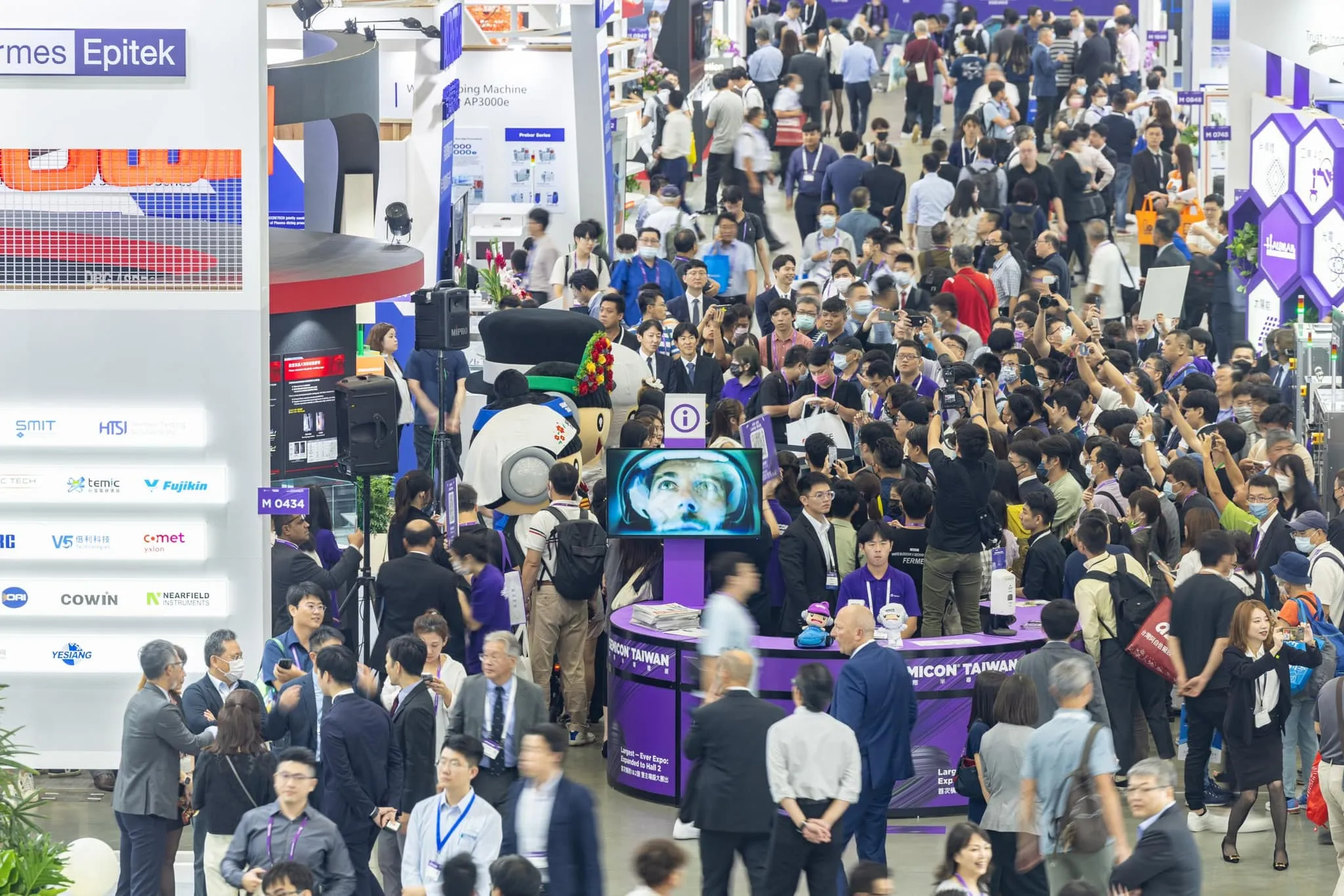
● Significant Scale-Up Aims to Bolster Global Semiconductor Ecosystem Ties: SEMICON Taiwan 2025 is set to break records, bringing together over 1,100 companies and industry partners from 56 countries, with more than 100,000 visitors expected to explore the latest semiconductor trends. For the first time, the event expands into a full International Semiconductor Week, featuring global forums on September 8 – 9 to deepen technical exchange and cross-border collaboration. A record 17 Country Pavilions further highlight Taiwan’s crucial role in the global semiconductor supply chain, providing an enhanced platform for industry dialogue and partnerships.

● Showcasing Cutting-edge Technologies and Delivering the World’s Most Comprehensive Semiconductor Insights: Fueled by soaring AI and HPC demand, the semiconductor industry is entering the ‘Hyper Moore’s Law’ era, advancing chip architectures beyond the nanometer scale into the angstrom era and driving greater system integration and miniaturization in packaging. As a leading innovation platform, SEMICON Taiwan 2025 will spotlight breakthroughs in advanced manufacturing and cutting-edge packaging technologies such as 3DIC, chiplets, and FOPLP. The event will also cover key innovations including silicon photonics, high-bandwidth memory (HBM), and backside power delivery networks (BSPDN), highlighting technologies that are reshaping the industry and defining the future of semiconductors.
As AI investment and cross-sector collaboration grow, the semiconductor ecosystem is moving toward integrated co-creation. SEMICON Taiwan gathers over 200 leading companies and experts in more than 20 forums, offering in-depth industry insights and driving technology into practice.

● Driving Future Competitiveness Through Geostrategy, Talent Development, Sustainability, and Cybersecurity: In response to global supply chain restructuring and geopolitical challenges, this year’s forum will debut Geostrategy as a new theme. International delegations at SEMICON Taiwan will engage in bilateral and multilateral dialogues with Taiwan’s government and industry leaders, while dedicated sessions on semiconductor geostrategy will focus on enhancing supply chain resilience and global collaboration.
As AI talent competition intensifies and net-zero goals advance, SEMICON Taiwan 2025 will bolster industry resilience for the long term. The Workforce Development Pavilion will launch the SEMI 20 UNDER 40 Awards and hands-on activities to inspire future talent, while the High-Tech Facility Pavilion and expanded Green Manufacturing Area will highlight sustainable technologies and ESG leadership.
As a global leader in advanced manufacturing, innovation, and cybersecurity, Taiwan sets industry benchmarks as SEMI advances security frameworks for a safer ecosystem. With a focus on talent, sustainability, and collaboration, SEMICON Taiwan powers the next 30 years of sustainable innovation.

Registration for SEMICON Taiwan 2025 opens on June 18. Industry professionals can apply for free visitor discount codes through August 31. Super early bird registration for the International Semiconductor Forum is also available now, offering an exclusive 30% discount for a limited time. For more details, visit the Official website.
*Source: SEMI Report, June 5, 2025
 

Main Theme of SEMICON Taiwan 2025_Leading with Collaboration. Innovating with the World

▲Main Theme of SEMICON Taiwan 2025_Leading with Collaboration. Innovating with the World

SEMICON Taiwan 2025 Is Set to Break Records With 100,000+ Visitors Expected

▲SEMICON Taiwan 2025 Is Set to Break Records With 100,000+ Visitors Expected


About SEMI

SEMI® is the global industry association for the semiconductor and electronics design and manufacturing supply chain, connecting over 3,000 member companies and 1.5 million professionals worldwide. Through diverse initiatives including policy advocacy, talent development, sustainability, and supply chain management, SEMI facilitates collaboration among members to address critical industry challenges. SEMI’s SEMICON® Taiwan exhibitions and events, technical communities, standardization, and market intelligence to empower members in driving business growth and innovation across design, devices, equipment, materials, services, and software, enabling smarter, faster, and more secure electronic technologies. For more information, visit  www.semi.org  or join SEMI Facebook, and SEMI LinkedIn.

MILPITAS, Calif. – June 24, 2025 – SEMI, the global industry association representing the electronics manufacturing and design supply chain, today announced the strategic acquisition of select assets from Linx Consulting, a leading market intelligence and consulting firm to the semiconductor, display, photovoltaic, MEMS, energy, and nanotechnology industries. As part of the acquisition, SEMI will integrate Linx Consulting’s market reports and conferences, such as the Surface Preparation and Cleaning Conference (SPCC) and the Electronic Specialty Gases & Systems (ESGS), into its product portfolio. The acquisition of these assets strengthens SEMI Market Intelligence in specialty materials and manufacturing processes, offering deeper insights to its global members and the broader industry.

“Acquiring Linx Consulting market reports marks a significant milestone in our mission to provide comprehensive and actionable market insights to our global members,” said Clark Tseng, Senior Director of Market Intelligence at SEMI. “Linx Consulting’s expertise, particularly in semiconductor and electronics materials market analysis, and established conferences will greatly enhance our ability to serve the industry.”

Integrating Linx Consulting’s renowned industry reports and market forecasts with SEMI’s extensive global network and resources will deliver unparalleled market intelligence and analysis to the semiconductor and electronics materials sectors. Going forward, customers can expect the same high-quality intelligence and insightful conferences they have relied on from Linx Consulting.

“There is great synergy with SEMI, and we believe they are the most qualified organization to further develop and enhance our market reports and conferences with their trusted team and global influence,” said Mark Thirsk, Managing Partner at Linx Consulting. “We are confident that this transition will bring even greater value to our clients.”

“We are dedicated to ensuring a seamless transition and maintaining the high standards of quality and service that our customers expect,” said Mike Corbett, Managing Partner at Linx Consulting. “As such, we will carefully manage this transition to ensure continuity and uphold our commitment to excellence.”

During the Strategic Materials Conference (SMC) 2025 in San Jose, an annual gathering of materials and supply chain experts in the semiconductor ecosystem, SEMI launched a new “Wafer Fab Materials Quarterly” report in collaboration with Linx Consulting. This report equips industry professionals with actionable insights into economic trends, material usage, sales performance, and capacity forecasts. The report will be available in July 2025. 

For details about SEMI reports on other semiconductor sectors, visit SEMI Market Data or contact the SEMI Market Intelligence team at [email protected].

About SEMI

SEMI® is the global industry association connecting over 3,000 member companies and 1.5 million professionals worldwide across the semiconductor and electronics design and manufacturing supply chain. We accelerate member collaboration on solutions to top industry challenges through Advocacy, Workforce Development, Sustainability, Supply Chain Management and other programs. Our SEMICON® expositions and events, technology communities, standards and market intelligence help advance our members’ business growth and innovations in design, devices, equipment, materials, services and software, enabling smarter, faster, more secure electronics. Visit www.semi.org, contact a regional office, and connect with SEMI on LinkedIn and X to learn more.

About Linx Consulting

Linx Consulting is a leading provider of market intelligence and consulting services to the semiconductor and electronics industries. Known for its in-depth market reports and high-caliber conferences, Linx Consulting has been a trusted partner to industry leaders for over two decades.

Association Contact

Sherrie Gutierrez/SEMI
Phone: 1.831.889.3800 
Email: [email protected]

Brussels, Belgium – June 19, 2025 – A pan-European consortium dedicated to developing sustainable processes and technologies for the semiconductor manufacturing industry today announced the launch of the GENESIS project. This integrated, large-scale initiative aims to enable Europe’s chip industry to meet its sustainability goals—from materials development to final waste treatment.

Genesis

Coordinated by CEA-Leti, the three-year project brings together 58 partners spanning the entire European semiconductor value chain, from large enterprises and subject matter experts (SMEs) to research institutes, universities, and industry associations. GENESIS will drive innovative solutions in emission control, eco-friendly materials such as alternatives to per- and polyfluoroalkyl substances (PFAS), waste minimization, and raw material reuse, directly aligned with the European Green Deal and European Chips Act.

“GENESIS partners are committed to fruitful and constructive collaboration throughout the duration of the project to deliver lasting impact on the European semiconductor ecosystem,” said Laurent Pain, Sustainable Electronics Program Director at CEA-LETI, and Coordinator of the GENESIS project.

SEMI Europe will oversee the dissemination of communication and promotion of activities to raise awareness and understanding of the importance of sustainable semiconductor manufacturing technologies across both industry and academia.

SEMI“The European semiconductor industry recognizes the urgency of seeking alternatives to substances of high concern, and reducing greenhouse gas emissions,” said Laith Altimime, President of SEMI Europe. “With semiconductor demand rising, the European Commission's funding of crucial initiatives such as GENESIS drives sustainable innovative solutions.”
The GENESIS consortium will focus on scientific research to facilitate the industry's transition toward sustainable manufacturing throughout the project’s three-year term. Additionally, the initiative will deliver added value through knowledge sharing, job creation, and positive socioeconomic impacts across the European regions represented by project partners.

45 Sustainability Innovations Driven by Four Strategic Pillars

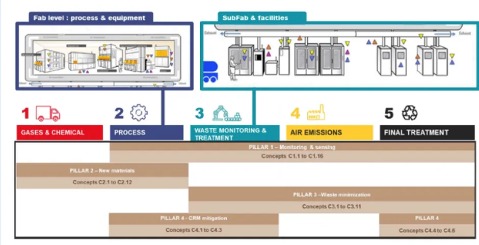
Pain noted that the GENESIS project team expects to deliver approximately 45 sustainability-driven innovations covering the semiconductor lifecycle, guided by four strategic pillars that form the technological foundation of GENESIS’s vision for a green European semiconductor industry:

  • Pillar 1 – Monitoring & Sensing: Real-time emissions tracking, traceability, and process feedback systems,
  • Pillar 2 – New Materials: PFAS-free chemistries and low-GWP alternatives for advanced semiconductor processes,
  • Pillar 3 – Waste Minimization: Innovations in recycling (solvent, gas, slurries), reuse, and sustainable replacements, and
  • Pillar 4 – Critical Raw Materials Mitigation: Strategies to reduce dependency on CRM and strengthen resource security.

Complimenting these pillars, the project’s objectives establish an overall framework that includes deploying sensor-integrated abatement systems to reduce PFAS and greenhouse gas emissions. It also aims to position Europe as a leader in green semiconductor innovation by aligning supply-chain practices with environmental regulations.

A Green Fit for Europe’s Chips Agenda

“The launch of the GENESIS project marks a critical step toward aligning Europe’s semiconductor ambitions with its climate commitments,” said Anton Chichkov, head of programs at Chips Joint Undertaking (Chips JU), a public-private partnership created to bolster Europe's semiconductor industry by fostering collaboration between the EU, member states, and the private sector. 

“As chips become the backbone of everything from AI to energy systems, their environmental footprint is rapidly growing,” said Chichkov. “GENESIS responds to this urgent challenge by pioneering sustainable alternatives in materials, waste reduction, and resource efficiency. Through this initiative, Europe is not only investing in cleaner technologies—it’s positioning itself as a global leader in green semiconductor manufacturing.”

With a budget of close to €55 million, the GENESIS project is co-funded through the Chips Joint Undertaking by the European Commission, participating EU member states, and the Swiss State Secretariat for Education, Research and Innovation (SERI).

The Five Critical Stages in Chip-Making Lifecycle Addressed by GENESIS

The GENESIS integrated roadmap outlines five critical stages in the semiconductor manufacturing lifecycle—materials (PFAS-free alternatives & gases and chemicals, processes, waste monitoring & treatments, air emissions, and final treatments—where environmental impact can be minimized.

This structured approach guides the project’s efforts to reduce emissions, eliminate harmful substances, and enable material recovery through innovation in sensing, materials, waste reduction, and raw material reuse.

About GENESIS

GENESIS (GENErate a Sustainable Industry for Semiconductors) is a pan-European project co-funded by the EU, Chips JU, Member States, and the Swiss State Secretariat for Education, Research and Innovation (SERI). Coordinated by CEA-Leti, it includes 58 partners from across Europe, focused on leading semiconductor manufacturing into a circular economy model, which aims to minimize waste and maximize resource reuse, and a low-impact, innovation-driven industry. https://www.genesiseu.eu/ 

About SEMI

SEMI® is the global industry association connecting over 3,000 member companies and 1.5 million professionals worldwide across the semiconductor and electronics design and manufacturing supply chain. We accelerate member collaboration on solutions to top industry challenges through Advocacy, Workforce Development, Sustainability, Supply Chain Management, and other programs. Our SEMICON® expositions and events, technology communities, standards, and market intelligence help advance our members’ business growth and innovations in design, devices, equipment, materials, services, and software, enabling smarter, faster, more secure electronics. Visit www.semi.org, contact a regional office, and connect with SEMI on LinkedIn and X to learn more.

Association Contacts

Jatin Mendiratta / SEMI Europe
Phone: +49 160 402 8899
Email: [email protected]

Samer Bahou / SEMI Corporate
Phone: +1 408 943 7870
Email: [email protected]