downloadGroupGroupnoun_press release_995423_000000 copyGroupnoun_Feed_96767_000000Group 19noun_pictures_1817522_000000Member company iconResource item iconStore item iconGroup 19Group 19noun_Photo_2085192_000000 Copynoun_presentation_2096081_000000Group 19Group Copy 7noun_webinar_692730_000000Path
Skip to main content
Default Banner Image

SEMI Press Release

ID
semi-press-release

MILPITAS, Calif. and WEST LAFAYETTE, Ind. — May 21, 2025 — SEMI, the industry association serving the global semiconductor and electronics design and manufacturing supply chain, today announced it has partnered with Purdue University to launch an online course series focused on artificial intelligence (AI) and data analysis techniques for the semiconductor industry. Available through the SEMI University learning platform, the courses were developed to equip semiconductor professionals to integrate AI and data-driven approaches in today’s competitive industry landscape. 

The full list of 10 online, self-paced SEMI U AI and data analysis courses in partnership with Purdue University are now available. The courses are taught by industry experts and offer a certificate from Purdue upon successful completion of each course module.

“As global demand for semiconductors steadily grows over time, SEMI U is supporting the industry’s workforce needs through its flexible learning platform,” said Shari Liss, Vice President of Global Workforce Development and Initiatives at SEMI. “The rapid evolution of the industry warrants both extensive workforce development efforts as well as AI automation for existing operations. Our partnership with Purdue University, a globally recognized leader in semiconductor engineering and technology education, allowed us to tackle both considerations with these courses that teach essential skills in AI, machine learning, and data analytics.”

“There’s an immediate need for semiconductor-focused learning opportunities as manufacturing expands in the United States,” said Dimitrios Peroulis, Purdue University Senior Vice President for Partnerships and Online. “Staffing new facilities with capable talent requires education that keeps pace with the direction of the industry. This platform of SEMI U courses offers industry professionals and students an accessible way to gain valuable, on-demand training in one of the world’s fastest-growing sectors, as well as important related fields such as AI and data analytics and analysis.”

SEMI U’s online series with Purdue University includes: 

About SEMI University and the SEMI Workforce Development Program

The SEMI University learning platform offers more than 800 online courses specifically created for the semiconductor industry, providing an easy-to-use online training program in multiple languages for employees ranging from recently hired facility operators to experienced technicians, engineers and non-technical staff. 

SEMI has offered in-person training and technology trend updates more than 50 years, and it hosts webinars covering SEMI standards, market dynamics and semiconductor manufacturing and design best practices. SEMI University builds on this experience and adds to the association’s holistic Workforce Development program offered by the SEMI Foundation. The non-profit arm of SEMI, the SEMI Foundation drives initiatives to increase awareness of semiconductor industry careers, connect member companies with university students for mentoring and internships, attract and train military veterans, and develop a more diverse and inclusive workforce.

About SEMI

SEMI® is the global industry association connecting over 3,000 member companies and 1.5 million professionals worldwide across the semiconductor and electronics design and manufacturing supply chain. We accelerate member collaboration on solutions to top industry challenges through Advocacy, Workforce Development, Sustainability, Supply Chain Management and other programs. Our SEMICON® expositions and events, technology communities, standards and market intelligence help advance our members’ business growth and innovations in design, devices, equipment, materials, services and software, enabling smarter, faster, more secure electronics. Visit www.semi.org, contact a regional office, and connect with SEMI on LinkedIn and X to learn more.  

About Purdue University

Purdue University is known for its excellence, scale, and impact in semiconductor education and research. Purdue leads the 33-university SCALE network, which is developing a semiconductor workforce for the defense sector. Purdue’s Semiconductor Degrees Program, guided by 40 senior semiconductor leaders, is developing the semiconductor workforce for the commercial sector. A strong, critical mass of researchers spans the full stack of semiconductors R&D, from materials and devices, to circuits, systems, architecture, and advanced packaging integration. Led by the Atalla Institute for Advanced System Integration and Packaging, the Birck Nanotechnology Center, the Center for Secure Microelectronics Ecosystems, the Institute for CHIPS and AI, and supported by the nanoHUB infrastructure for data services and AI, Purdue plays an active role in many national R&D programs.

Association Contact

Sherrie Gutierrez/SEMI Corporate
Phone: 1.831.889.3800
Email: [email protected]

MILPITAS, Calif. – May 19, 2025 – According to the Q1 2025 Semiconductor Manufacturing Monitor (SMM) Report released by SEMI in collaboration with TechInsights, the global semiconductor manufacturing industry entered 2025 with typical seasonal patterns. However, looming tariff threats and evolving supply chain strategies are expected to create atypical seasonality for several industry segments as the year progresses.

Despite heightened trade policy risks, current data for the first quarter of 2025 indicate that electronics and integrated circuit (IC) sales have not been directly impacted by the newly announced tariffs. Electronics sales declined 16% quarter-over-quarter (QoQ) in Q1 2025 and remained flat year-over-year (YoY), consistent with traditional seasonal patterns. IC sales contracted by 2% QoQ but posted a robust 23% YoY increase, reflecting ongoing investment in AI and high-performance computing infrastructure.

semi & techinsights“While the first quarter of 2025 did not see a direct impact from new tariffs on electronics and IC sales, the uncertainty around global trade policies is prompting some companies to accelerate shipments and others to pause investments,” said Clark Tseng, Senior Director of Market Intelligence at SEMI. “This push-pull dynamic could lead to atypical seasonality for the remainder of the year as the industry adapts to shifting supply chain and tariff landscapes.”
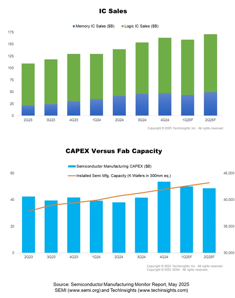

Semiconductor capital expenditures (CapEx) declined 7% QoQ but surged 27% YoY, as manufacturers continued to invest heavily in leading-edge logic, high-bandwidth memory (HBM) and advanced packaging to support AI-driven applications. Memory-related CapEx soared 57% YoY in Q1 2025, while non-memory CapEx expanded by 15% YoY, underscoring the industry’s focus on innovation and resilience.

Wafer fab equipment (WFE) spending rose 19% year-over-year in Q1 2025 and is projected to increase another 12% in Q2, driven by strong investments in advanced logic and memory production to support the rapid adoption of AI semiconductors. Test equipment billings surged 56% year-over-year in Q1 and are expected to grow by 53% in Q2, reflecting the heightened complexity and stringent performance requirements of AI and HBM chip testing. Assembly and packaging equipment also registered double-digit growth, benefiting from the industry’s push toward higher-density integration and advanced packaging solutions.

“The WFE market is poised for steady growth driven by government investments and semiconductor advancements, particularly in AI and emerging technologies,” said Boris Metodiev, Director of Market Analysis at TechInsights. “However, geopolitical uncertainties, including export restrictions and potential tariffs, pose significant risks that could impact this positive trajectory.”

Aligned with the growth in capital equipment investments, global installed wafer fab capacity is on the rise and is projected to surpass 42.5 million wafers per quarter (in 300mm wafer equivalents), reflecting a 2% QoQ and 7% YoY increase in Q1 2025. China continues to lead all regions in capacity expansion, though the pace of growth is expected to moderate in the coming quarters. Notably, Japan and Taiwan are experiencing the strongest quarterly capacity gains, driven by significant investments in power semiconductor manufacturing in Japan and the ramp-up of a leading-edge foundry in Taiwan.

Looking ahead, SEMI and TechInsights expect the industry to experience atypical seasonal patterns in 2025 as companies navigate the dual challenges of trade policy uncertainty and supply chain adaptation. While demand for AI and data center technologies remains a bright spot, other segments may see delayed investment or demand shifts as the market responds to evolving tariff and geopolitical uncertainties.


The Semiconductor Manufacturing Monitor (SMM) report provides end-to-end data on the worldwide semiconductor manufacturing industry. The report highlights key trends based on industry indicators including capital equipment, fab capacity, and semiconductor and electronics sales, and includes a capital equipment market forecast. The SMM report also contains two years of quarterly data and a one-quarter outlook for the semiconductor manufacturing supply chain including leading IDM, fabless, foundry, and OSAT companies. An SMM subscription includes quarterly reports. 

Download a sample Semiconductor Manufacturing Monitor report.  

For more information on the report or to subscribe, please contact the SEMI Market Intelligence Team at [email protected]. Details on SEMI market data are available at SEMI Market Data.  

About SEMI

SEMI® is the global industry association connecting over 3,000 member companies and 1.5 million professionals worldwide across the semiconductor and electronics design and manufacturing supply chain. We accelerate member collaboration on solutions to top industry challenges through Advocacy, Workforce Development, Sustainability, Supply Chain Management and other programs. Our SEMICON® expositions and events, technology communities, standards and market intelligence help advance our members’ business growth and innovations in design, devices, equipment, materials, services and software, enabling smarter, faster, more secure electronics. Visit www.semi.org, contact a regional office, and connect with SEMI on LinkedIn and X to learn more.

Association Contact

Sherrie Gutierrez/SEMI
Phone: 1.831.889.3800 
Email: [email protected]

MILPITAS, Calif. — May 14, 2025 — SEMI today announced the election of a new member to the SEMI North America Advisory Board (NAAB), Rosemary Steen Hoffman, Chief Executive Officer, SACHEM, Inc., a premier supplier of high-purity, precision-based chemistries.

SEMIThe Board appointment took effect on April 14, 2025. Members serve a three-year term. The principal advocate for member companies located in North America, the NAAB provides guidance on SEMI Americas programs designed to advance their business interests and address significant challenges in the electronics manufacturing and design supply chain. 

“We are thrilled to welcome Rosemary Steen Hoffman to the SEMI North America Advisory Board,” said Joe Stockunas, President of SEMI Americas. “With her exceptional leadership and over 30 years of experience in the global chemical industry, Rosemary brings a proven track record of driving innovation, growth, and operational excellence, offering valuable insight and a unique perspective to the NAAB.”

Prior to her role as CEO of SACHEM, Hoffman held key leadership positions in the organization, including Chief Operating Officer and Vice President for Sales and Marketing. She is a transformative leader known for building and inspiring high-performing teams while fostering a culture of innovation, accountability, and continuous improvement. Beyond her professional achievements, Hoffman is deeply committed to community service and philanthropy, currently serving on the Board of Directors for Ascension Seton Hospital and previously for Caritas in Austin. She holds an MBA from Anderson School of Business at UCLA and a B.S. in Chemical Engineering from Pennsylvania State University.

About SEMI

SEMI® is the global industry association connecting over 3,000 member companies and 1.5 million professionals worldwide across the semiconductor and electronics design and manufacturing supply chain. We accelerate member collaboration on solutions to top industry challenges through Advocacy, Workforce Development, Sustainability, Supply Chain Management and other programs. Our SEMICON® expositions and events, technology communities, standards and market intelligence help advance our members’ business growth and innovations in design, devices, equipment, materials, services and software, enabling smarter, faster, more secure electronics. Visit www.semi.org, contact a regional office, and connect with SEMI on LinkedIn and X to learn more.  

Association Contact

Sherrie Gutierrez/SEMI Corporate
Phone: 1.831.889.3800
Email: [email protected] 

Seoul, Korea. — May 12, 2025 — The Strategic Materials Conference (SMC) Korea 2025 is set to convene on May 14 at the Suwon Convention Center in Gyeonggi-do, South Korea, bringing together leading experts and innovators to highlight the critical role of materials innovation in addressing the performance, efficiency, and scalability requirements of AI-enabled semiconductor devices. Registration is open.

smc korea 2025Themed Empowering the AI Era: Advancements in Next-Generation Memory and Materials, SMC Korea 2025 will feature 9 global visionaries presenting on advanced materials, technology trends, and market forecasts. A panel discussion and networking opportunities will round out the day’s agenda, providing a platform for deep cross-industry collaboration.

SMC Korea 2025 will also feature the following sessions:

  • 3D DRAM/CFET – Experts from Samsung Electronics, imec, Hanyang University, and Air Liquide will share insights into the materials innovations driven by the advancement of next-generation memory semiconductor technologies such as 3D DRAM and CFET.
  • The Future of Semiconductor Materials – Visionaries from Applied Materials, Linx Consulting, Entegris, Chipmetrics and SK hynix will discuss the technological innovation roadmap for semiconductor materials required in advanced manufacturing processes for high bandwidth memory (HBM) and other leading-edge technologies.

SMC Korea 2025 Sponsors

  • Dongwoo Fine-chem
  • JSR Electronic Materials Korea
  • Huntsman Performance Products
  • UP Chemica
  • DuPont Electronics & Industrial
  • Dongjin Semichem
  • SK trichem
  • TEMC
  • Entegris
  • Air Liquide Solutions Korea

About SEMI

SEMI® is the global industry association connecting over 3,000 member companies and 1.5 million professionals worldwide across the semiconductor and electronics design and manufacturing supply chain. We accelerate member collaboration on solutions to top industry challenges through Advocacy, Workforce Development, Sustainability, Supply Chain Management and other programs. Our SEMICON® expositions and events, technology communities, standards and market intelligence help advance our members’ business growth and innovations in design, devices, equipment, materials, services and software, enabling smarter, faster, more secure electronics. Visit www.semi.org, contact a regional office, and connect with SEMI on LinkedIn and X to learn more.  

Association Contacts

Jaegwan Shim/SEMI Korea
Phone: 82+2.531.7804
Email: [email protected] 

Sherrie Gutierrez/SEMI Corporate
Phone: 1.831.889.3800
Email: [email protected] 

MUNICH, Germany ─ May 1, 2025 ─ SEMI Europe announced the opening of the call for abstracts for SEMICON Europa 2025, to be held November 18-21 at Messe München in Munich, Germany. Selected speakers will share their expertise at the Advanced Packaging Conference (APC), MEMS & Imaging Sensors Summit, and during presentations on the show floor. 

SEMICON EuropaEurope’s premier event connecting the entire electronics design and manufacturing supply chain, SEMICON Europa 2025 will gather industry experts and innovators to explore how international collaboration is driving technological innovation, economic resilience, and sustainability across Europe’s semiconductor ecosystem. The exhibition and conference will be co-located with productronica.  

Call for Abstracts

Advanced Packaging Conference (APC) ─ Key Enabler for System Performance

Advanced packaging technologies—including 2.5D and 3D stacking, chiplet integration, and heterogeneous packaging—are revolutionizing system performance by delivering greater processing power and energy efficiency. Innovations in advanced materials and interconnects are further reducing signal loss and latency, enabling high-performance computing and AI at scale. Abstracts are invited on key topics including advanced materials and processes for packaging, power and thermal management in 2.5D/3D packaging, packaging innovations for silicon photonics, and testing inspection and metrology.

MEMS & Imaging Sensors Summit  ─ Industry Meets Innovative Ideas

Entrepreneurs, startups, graduates, and newcomers will showcase their research and early-stage products. Topics of interest include new applications and use cases for MEMS and sensors, advancements in technology and materials, smart MEMS and AI integration, MEMS-photonics co-integration, alternative imaging sensor architectures, and foundry offers for start-ups. 

Pre-recorded Innovation Presentations ─ Global Collaborations for European Economic Resilience

SEMI Europe will also highlight microelectronics and semiconductors innovations in short pre-recorded messages, pitches and product announcements that will be aired on SEMICON Europa 2025 main stages during networking sessions and on the final day of the exhibition. Projects of interest include sustainability and green technologies, diversity and inclusion, semiconductor advancements in aerospace, defense and automotive applications, as well as smart manufacturing, cybersecurity and more. 

Presentation abstracts, biographies, and headshots must be submitted in English through the SEMICON Europa 2025 Call for Abstracts portal by Friday, June 20, 2025. Selected presenters will be notified in August 2025. 

For more details, please visit the SEMICON Europa 2025 website and connect with SEMI Europe on LinkedIn or YouTube @SEMIEurope (#SEMICONEuropa). 

SEMICON Europa Premier Sponsors 

  • Platinum: MANN+HUMMEL, Merck KGaA, Darmstadt, Germany
  • Gold: Edwards
  • Event: CTP, MKS-Atotech, INFICON, and SCREEN

About SEMI 

SEMI® is the global industry association connecting over 3,000 member companies and 1.5 million professionals worldwide across the semiconductor and electronics design and manufacturing supply chain. We accelerate member collaboration on solutions to top industry challenges through Advocacy, Workforce Development, Sustainability, Supply Chain Management and other programs. Our SEMICON® expositions and events, technology communities, standards and market intelligence help advance our members’ business growth and innovations in design, devices, equipment, materials, services and software, enabling smarter, faster, more secure electronics. Visit www.semi.org, contact a regional office, and connect with SEMI on LinkedIn and X to learn more.  

Contact Information: 

Sitong He / SEMI Europe  
Phone: +49 151 55462638
Email: [email protected]   

Sherrie Gutierrez / SEMI Corporate 
Phone: +1 831 889 3800  
Email: [email protected] 

DRESDEN, Germany — April 30, 2025 — Leading experts in 3D integration and systems for semiconductor manufacturing applications will gather at the annual SEMI 3D & Systems Summit, June 25-27, 2025, in Dresden. The Summit will offer insights into the latest heterogeneous integration innovations that are strengthening Europe’s semiconductor resilience and powering the next generation of intelligent systems. Registration is open.  

3d system summitThemed Heterogenous Integration: Bolstering Europe's Resilience, this year’s Summit will feature an expanded program covering geopolitical dynamics, market trends, chiplet design, as well as the latest advancements in chiplet applications and hybrid bonding techniques.

“We look forward to welcoming industry leaders, innovators, and researchers to showcase their latest technologies and developments at the 3D & Systems Summit,” said Laith Altimime, President of SEMI Europe. “As Europe advances in chiplet architectures, hybrid bonding, and co-packaged optics, the Summit provides a unique platform to drive collaboration and highlight the innovations shaping the future of semiconductors.”

3D & Systems Summit Sessions 

NextGen Talent: Empowering Careers, Driving Growth

Featuring insights from semiconductor leaders, educators, and students, this session will highlight best practices for attracting, developing, and retraining top talent. Experts will discuss strategies that foster innovation, bridge talent gap, and create meaningful career opportunities—key to securing Europe’s continued leadership in the semiconductor industry.

Session 1: Geopolitical Dynamics and Market Trends

Executive leaders will examine how geopolitical dynamics are reshaping the semiconductor industry, highlighting Europe’s strategic role amid global demand shifts and supply chain disruptions.

Session 2: Chiplet Applications: System Level Architectures

Industry experts will explore the diverse applications of chiplet technology in various fields, highlighting the conceptual aspects of design and 3D integration.

Session 3: Hybrid Bonding - Die to Wafer

Specialists will focus on die-to-wafer hybrid bonding and its role in enabling advanced 3D integration, with insights into scalability, cost-effectiveness, and the roadmap for industry adoption.

Session 4: Hybrid Bonding - Wafer to Wafer

Experts will discuss wafer-to-wafer hybrid bonding technologies and examine the current state of these technologies as well as the technical and market challenges they face. 

Session 5: Photonics and Co-Package Optics

Industry leaders will share insights into the integration of photonics and co-package optics, and how these advancements can drive innovation and efficiency across diverse industries.

Session 6: European Readiness: Design, Materials, Manufacturing

Visionaries will explore the design, materials, and manufacturing scalability of technologies, highlighting key challenges, cost-effective factors, and innovative solutions for advancing 3D integrated circuits and chiplet production.

Global Leaders to Present 

3D & Systems Summit presenters include experts from these global leaders:   

  • Adeia

  • ASML

  • Besi

  • Bosch

  • CEA-Leti

  • Confovis

  • ETEL S.A.

  • European Semiconductor Manufacturing Company (ESMC)

  • EV Group

  • Fraunhofer

  • imec

  • Infinitesima

  • Intel

  • KLA

  • Lam Research

  • NXP Semiconductors

  • RANOVUS

  • SUSS MicroTec

  • TechSearch International

  • Yole Group

Exhibition and Business Networking 

The 3D & Systems Summit will also feature business-to-business matchmaking and networking for participants to explore new partnerships and other business opportunities.  

To reserve an exhibition space, contact [email protected]. 

This year’s networking reception will take place at the Hilton Dresden on the first day of the event, and the annual networking dinner will be held on the Elbe River cruise. 

Networking dinner registration is reserved exclusively for 3D & Systems Summit 2025 participants. Guests may register their spouse for dinner through the registration link.   

3D Summit premium sponsors: Adeia, ASE, Comet, Confovis, CTP, EV Group, HEIDENHAIN, imec, Lam Research, MKS Atotech

For more details, please visit the 3D & Systems Summit 2025 website and connect with SEMI Europe on LinkedIn or YouTube @SEMIEurope (#3DSummit).  

About SEMI 

SEMI® is the global industry association connecting over 3,000 member companies and 1.5 million professionals worldwide across the semiconductor and electronics design and manufacturing supply chain. We accelerate member collaboration on solutions to top industry challenges through Advocacy, Workforce Development, Sustainability, Supply Chain Management and other programs. Our SEMICON® expositions and events, technology communities, standards and market intelligence help advance our members’ business growth and innovations in design, devices, equipment, materials, services and software, enabling smarter, faster, more secure electronics. Visit www.semi.org, contact a regional office, and connect with SEMI on LinkedIn and X to learn more.  

Contact Information: 

Sitong He / SEMI Europe  
Phone: +49 151 55462638
Email: [email protected]   

Sherrie Gutierrez / SEMI Corporate 
Phone: +1 831 889 3800  
Email: [email protected] 

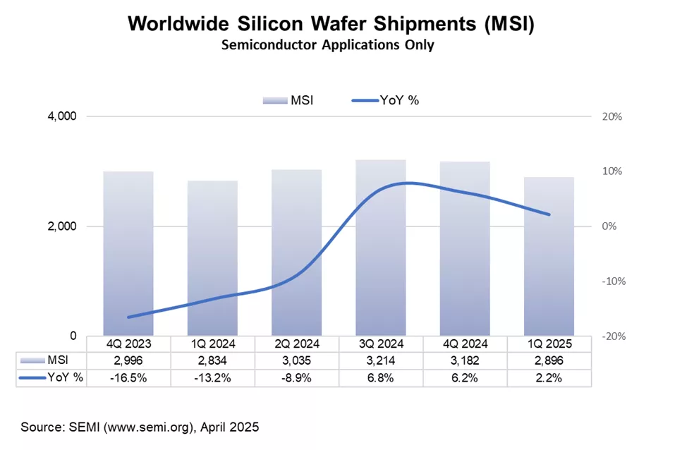
MILPITAS, Calif. — April 29, 2025 — Worldwide silicon wafer shipments increased 2.2% year-on-year (YoY) to 2,896 million square inches (MSI) from the 2,834 MSI recorded during the same quarter of 2024, the SEMI Silicon Manufacturers Group (SMG) reported in its quarterly analysis of the silicon wafer industry. Sequentially, shipments contracted 9.0% quarter-over-quarter from the 3,182 MSI recorded during the fourth quarter of last year impacted, primarily, by seasonality and accumulated inventory levels throughout the supply chain. 

SEMI“Q1 2025 silicon shipments indicated a 6% YoY growth in 300mm but showed a decline in 200mm and below wafer sizes,” said Lee Chungwei (李崇偉), Chairman of SEMI SMG and Vice President and Chief Auditor at GlobalWafers. “Despite an incremental increase in 300mm wafer shipments, demand for legacy devices remains weak, with inventory adjustments also contributing to a slowdown in shipments.”

 

Data cited in this release include polished silicon wafers, including those used as virgin test wafers, as well as epitaxial silicon wafers, and non-polished silicon wafers shipped by the wafer manufacturers to end users.


Silicon wafers are the fundamental building material for the majority of semiconductors, which are vital components of all electronic devices. The highly engineered thin disks are produced in diameters of up to 300mm and serve as the substrate material on which most semiconductors are fabricated.

The SMG is a sub-committee of the SEMI Electronic Materials Group (EMG) and is open to SEMI members involved in manufacturing polycrystalline silicon, monocrystalline silicon or silicon wafers (e.g., as cut, polished, epi). The SMG facilitates collective efforts on issues related to the silicon industry including the development of market information and statistics about the silicon industry and the semiconductor market.

For more information, visit SEMI Worldwide Silicon Wafer Shipment Statistics.

About SEMI

SEMI® is the global industry association connecting over 3,000 member companies and 1.5 million professionals worldwide across the semiconductor and electronics design and manufacturing supply chain. We accelerate member collaboration on solutions to top industry challenges through Advocacy, Workforce Development, Sustainability, Supply Chain Management and other programs. Our SEMICON® expositions and events, technology communities, standards and market intelligence help advance our members’ business growth and innovations in design, devices, equipment, materials, services and software, enabling smarter, faster, more secure electronics. Visit www.semi.org, contact a regional office, and connect with SEMI on LinkedIn and X to learn more.

Association Contact

Sherrie Gutierrez/SEMI
Phone: 1.831.889.3800 
Email: [email protected] 

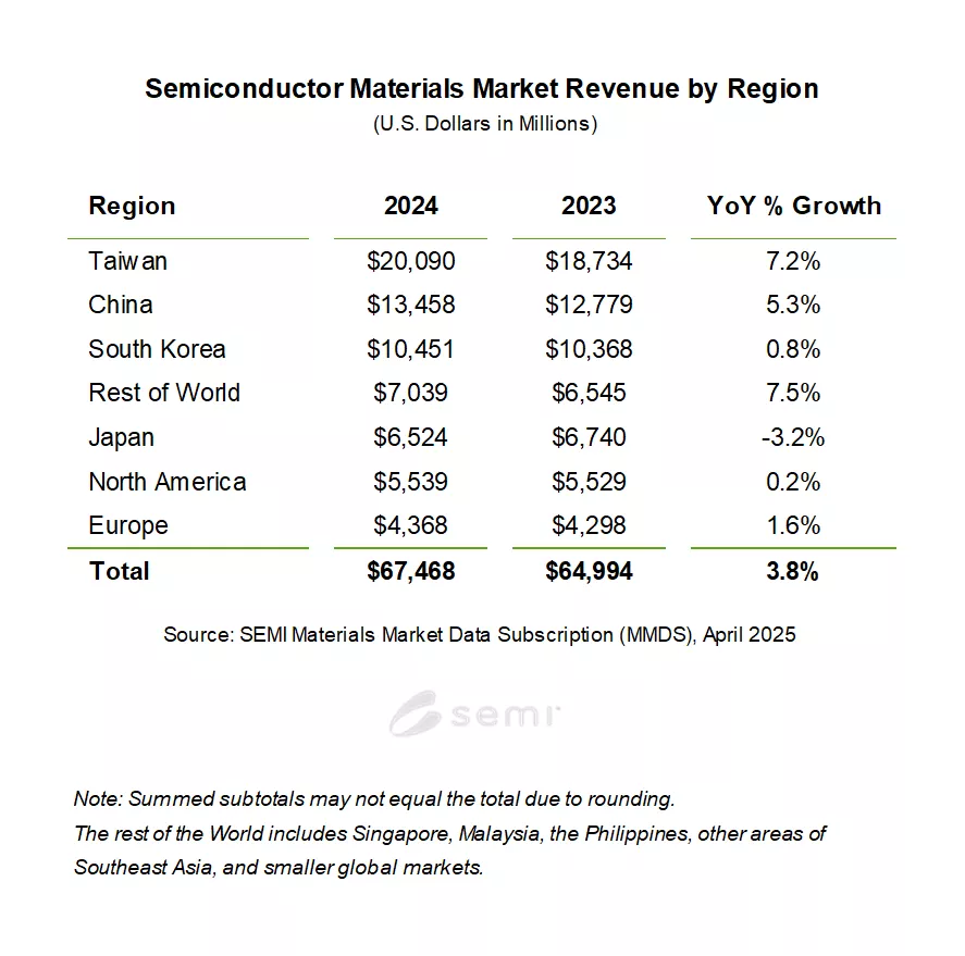
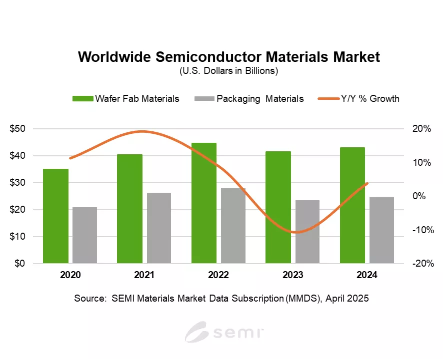
MILPITAS, Calif. — April 28, 2025 — Global semiconductor materials market revenue increased 3.8% to $67.5 billion in 2024, SEMI, the global industry association representing the electronics design and manufacturing supply chain, reported today in its Materials Market Data Subscription (MMDS). The recovery of the overall semiconductor market as well as the increasing demand for advanced materials for high-performance compute and high-bandwidth memory manufacturing supported 2024 materials revenue growth. 

SEMIWafer fabrication materials revenue increased 3.3% to $42.9 billion in 2024, while packaging materials revenue grew 4.7% to $24.6 billion last year. The chemical mechanical planarization (CMP), photoresist, and photoresist ancillaries segments experienced strong double-digit growth driven by increased complexity and number of processing steps required for advanced DRAM, 3D NAND flash and leading-edge logic integrated circuits (ICs). All semiconductor materials segments, except for silicon and silicon-on-insulator (SOI), registered year-on-year increases. The demand for silicon, particularly in the trailing edge segment, remained weak in 2024 as the industry continued to work through excess inventory, resulting in a 7.1% decline in silicon revenue in 2024. 
Taiwan, with $20.1 billion in revenue, was the world's largest consumer of semiconductor materials for the 15th consecutive year. China, at $13.5 billion in revenue, continued to register year-over-year growth, ranking second in 2024, while Korea followed as the third largest consumer with $10.5 billion in revenue. All regions, except for Japan, posted single-digit increases in 2024.  

The Materials Market Data Subscription (MMDS) from SEMI provides annual revenue with 10 years of historical data and a two-year forecast. The annual subscription includes quarterly updates for the materials segment and reports revenue for seven market regions (North America, Europe, Japan, Taiwan, South Korea, China and Rest of World). The report also features detailed historical data for silicon shipments and revenues for photoresist, photoresist ancillaries, process gases and lead frames.

For more information about the report or to subscribe, please contact the SEMI Market Intelligence Team at [email protected]. More details are also available on the SEMI Market Data webpage.  

Download a sample of the MMDS report. 

About SEMI

SEMI® is the global industry association connecting over 3,000 member companies and 1.5 million professionals worldwide across the semiconductor and electronics design and manufacturing supply chain. We accelerate member collaboration on solutions to top industry challenges through Advocacy, Workforce Development, Sustainability, Supply Chain Management and other programs. Our SEMICON® expositions and events, technology communities, standards and market intelligence help advance our members’ business growth and innovations in design, devices, equipment, materials, services and software, enabling smarter, faster, more secure electronics. Visit www.semi.org, contact a regional office, and connect with SEMI on LinkedIn and X to learn more.

Association Contact

Sherrie Gutierrez/SEMI
Phone: 1.831.889.3800 
Email: [email protected] 

MILPITAS, Calif. — April 15, 2025 — The 36th annual Advanced Semiconductor Manufacturing Conference (ASMC) 2025 will be held May 5-8, 2025, in Albany, New York, bringing together leaders in semiconductor manufacturing to explore cutting-edge advancements driving high-volume production and AI-powered innovation. Hosted by SEMI, this premier technical conference will feature more than 25 hours of programming, including technical and poster sessions, keynote talks, a panel discussion, a tutorial, and networking opportunities. Registration is now open.

asmcASMC 2025 will feature over 120 speakers addressing critical topics such as yield enhancement and methodologies, advanced metrologies, advanced process control, and advanced equipment processes and materials. The conference is co-chaired by Katie Lutker-Lee, Process Engineer at TEL Technology Center America and Samira Bagheri, Operations Manager at EMD Electronics.

ASMC 2025 Keynotes and Tutorial

Powering AI: Rising to the Challenge

  • Pavel Freundlich, Vice President & Chief Technology Officer of the Power Solutions Group, onsemi

Strategic Directions for Electronics Packaging

  • Subramanian S. Iyer, Distinguished Professor, UCLA 

Market Update

  • Robert Maire, President, Semiconductor Advisors

Materials Intelligence: Enabling the Future of Technology

  • Lu Gan, Senior Director, Head of Technology Strategy & Roadmap, EMD Electronics

ASMC 2025 Panel Discussion “High Volume Manufacturing in the Age of AI” 

Moderator:

  • Marie Tripp, Vice President, UNISERS

Panelists:

  • Deepa Desai, Director, Offering and Development Leader, IBM Semiconductor
  • Jason Komorowski, Senior Automation and Analytics Engineer, Intel
  • Pawitter Mangat, Vice President & Master Innovator, GlobalFoundries
  • Ross Kunz, Data Scientist, Idaho National Laboratory
  • Safa Kutup Kurt, Global Head of Plant Operations & Digital Transformation, EMD Electronics

ASMC 2025 technical and poster sessions will cover topics including:

  • Advanced Equipment Processes and Materials
  • Advanced Metrology
  • Advanced Process Control
  • Big Data Management and Machine Learning
  • Contamination Free Manufacturing
  • Defect Inspection and Reduction
  • Equipment Optimization
  • Factory Automation
  • Industrial and Factory Automation Design and Manufacturing Sustainability
  • Novel Devices and Advanced Patterning
  • Smart Manufacturing
  • Workforce Development
  • Yield Enhancement/Methodologies

Two programs will take place in conjunction with ASMC 2025

  • SEMI University (SEMI U) Workshop – May 5
    • Held for the first time in the Northeast, SEMI U will offer two in-person, instructor-led trainings: “Understanding Semiconductor Technology & Business” and “Advanced IC Packaging & Assembly.”
    • ASMC attendees receive a $100 discount on SEMI U registration.
  • Women in Semiconductors (WiS) – May 8
    • Open to all industry professionals, the WiS program will focus on actionable strategies to support career development and open internal growth opportunities.
    • ASMC registrants receive complimentary registration. 

For full conference details, please visit the ASMC website or contact Taylor Zhao at [email protected].

About SEMI

SEMI® is the global industry association connecting over 3,000 member companies and 1.5 million professionals worldwide across the semiconductor and electronics design and manufacturing supply chain. We accelerate member collaboration on solutions to top industry challenges through Advocacy, Workforce Development, Sustainability, Supply Chain Management and other programs. Our SEMICON® expositions and events, technology communities, standards and market intelligence help advance our members’ business growth and innovations in design, devices, equipment, materials, services and software, enabling smarter, faster, more secure electronics. Visit www.semi.org, contact a regional office, and connect with SEMI on LinkedIn and X to learn more.

Association Contact

Sherrie Gutierrez/SEMI
Phone: 1.831.889.3800
Email: [email protected]

TSMC and ASE Join Forces with 100+ Companies to Drive Silicon Photonics Technology Integration

【April 11, 2025 – Hsinchu】The SEMI Silicon Photonics Industry Alliance (SiPhIA) held the Bridging Light & Silicon: SEMI SiPhIA SIGs Kick-off & Seminar today, announcing the official launch of three Special Interest Groups (SIGs) aimed at integrating expertise from various sectors to formulate industry standards and accelerate technological innovation and commercialization. Mr. K.C. Hsu, Vice President of TSMC, and Dr. C.P. Hung, Vice President of ASE, attended as co-chairs of SEMI SiPhIA and delivered speeches to guide the SIGs. The seminar gathered over 200 industry leaders and experts to discuss the development of silicon photonics technology and the layout of global supply chain.

Silicon photonics has become a key technology driving the development of artificial intelligence (AI) due to its advantages in high-speed data transmission, high bandwidth, low power consumption, and high integration. However, it still faces challenges in manufacturing processes, packaging and testing to meet the rapidly increasing demand for data transmission. These challenges include shrinking chip sizes, reducing costs, minimizing energy loss in photonic integrated circuits, integrating photonic chips with advanced packaging, and developing effective solutions for heat dissipation. To overcome these challenges, SEMI SiPhIA established three SIGs to accelerate breakthroughs and commercialization of silicon photonics technology.

"The SEMI Silicon Photonics Alliance, centered on Taiwan's semiconductor industry, brings together over 110 leading domestic and international companies to develop the world's largest and most comprehensive international platform for silicon photonics technology collaboration," said Terry Tsao, Global Chief Marketing Officer and President of Taiwan, SEMI. “The alliance spans the entire supply chain, integrating cross-enterprise and cross-disciplinary expertise to fuel global innovation. Additionally, it has launched three SIGs focused on driving innovative technology breakthroughs and accelerating standardization efforts to jointly address the challenges posed by technological fragmentation.”

The Three SIGs Integrating Industry and Research to Establish a Complete Ecosystem, Focusing on Technological Breakthroughs and Commercialization

SEMI established the SiPhIA in September 2024 to advance silicon photonics technology. The alliance has formed three SIGs, spanning the entire industry ecosystem from system design and component manufacturing to packaging and testing.

  • SIG 1:System, Subsystems, and Silicon Photonics Technology Development, focusing on the future development trends in silicon photonics technology, including the design, manufacturing, and integration of silicon photonics chips, forming a complete silicon photonics ecosystem.
  • SIG 2:Advanced Packaging and Testing, focusing on heterogeneous integration and co-packaged optical application packaging and testing technologies, driving optical-electronic integration.
  • SIG 3:Equipment and Others, dedicated to developing and providing key equipment and technologies needed for the silicon photonics industry, focusing on process automation, including assembly, inspection technologies, and related equipment and innovative applications.

"TSMC will collaborate with the industry to develop a comprehensive roadmap for silicon photonics co-packaging solutions and work diligently to put it into practice," said K.C. Hsu, Vice President of TSMC and Co-Chair of SEMI SiPhIA. “We aim to overcome the technical bottlenecks by collaborating with alliance members through SIGs on cross-group projects to address specific technological challenges or application scenarios.”

"ASE has been deeply involved in silicon photonics technology development for over 15 years," said C.P. Hung, Vice President of ASE and Co-Chair of SEMI SiPhIA. “We will collaborate with alliance members through regular cross-group SIGs meetings and establish a shared database to ensure that the technological development strategies of different SIGs align with market demands and facilitate cooperation.”

"SEMI SiPhIA has successfully connected the industry and research sectors," said Wei-Chung Lo, Deputy General Director of Electronic and Optoelectronic System Research Laboratories at ITRI and Vice President of the SEMI SiPhIA. “ITRI has long been committed to silicon photonics technology research and development and plays a bridging role within the alliance, promoting the integration of research outcomes with industry demands to accelerate technology commercialization.

Outlook for Silicon Photonics Technology Development Roadmap for 2024 to 2027: Advancing from 2D to 3D Structures to Significantly Improve Energy Efficiency and Meet AI and Data Center Demands

Silicon photonics technology is regarded as a key technology for next-generation signal transmission. By integrating optical components onto silicon chips, this technology significantly enhances data transmission rates and reduces power consumption, addressing the growing demands for higher bandwidth and lower latency in data centers, 5G networks, high-performance computing, and other applications. The key discussion points of the SEMI SiPhIA include the 2024-2027 silicon photonics technology blueprint. It is expected that the technology will gradually evolve from 2D planar structures to 2.5D and 3D structures, significantly reducing energy consumption. As integration increases and energy efficiency improves, it will effectively meet the growing demands of high-speed data centers and AI computing.

Taiwan has laid a solid industrial foundation with its complete supply chain ecosystem and advanced packaging technology in the semiconductor industry. SEMI will continue to build various open platforms and integrate cross-disciplinary expertise to assist the industry in formulating clear development strategies and collaboratively promoting technological innovation.

About SEMI SiPhIA

The SEMI Silicon Photonics Industry Alliance (SEMI SiPhIA), launched by SEMI in 2024, serves as a vital platform for connecting the silicon photonics industry. It is dedicated to advancing technological innovation and application development, promoting the establishment of industry standards, and enabling key technological breakthroughs. Through knowledge sharing, resource integration, and technical exchange, SEMI SiPhIA strengthens collaboration among industry, government, academia, and research institutions, fostering a globally competitive silicon photonics ecosystem.

With the rapid advancement of AI and emerging technologies, the demand for high-speed data processing and transmission is surging—making silicon photonics a critical force driving industry upgrades. Since its founding, SEMI SiPhIA has attracted more than 110 industry partners and has actively promoted cooperation and innovation across the value chain. Looking ahead, SEMI SiPhIA will further deepen global supply chain integration, broaden international collaboration, and work closely with industry partners to co-create innovative solutions that fuel the sustainable growth of the entire industry.

About SEMI

Founded in 1970, SEMI operates 10 major offices globally and established the SEMI Taiwan in 1996. It connects over 3,000 member companies and 1.5 million professionals worldwide across the semiconductor and electronics design and manufacturing supply chain. Since its inception, SEMI Taiwan has annually hosted SEMICON® Taiwan, international summits, and various major technical forums, enhancing Taiwan's international influence and competitiveness. SEMI upholds the principles of objectivity and neutrality, acting as a semiconductor industry think tank for Taiwanese member companies. It fosters deep global exchanges among industry, government, academia, and research sectors, promoting Taiwan's semiconductor industry to align with global standards, and establishing a two-way communication platform.

SEMI Taiwan currently hosts 18 technical committees to drive industry growth and innovation in design, devices, equipment, materials, services, and software. It provides comprehensive market intelligence, standardization, policy advocacy, talent cultivation, sustainability development, supply chain management, and program assistance to empower members in facing industry challenges. For more information, visit www.semi.org or join SEMI Facebook and SEMI LinkedIn.

Media Contacts

SEMIElma Fang[email protected] 03-560-1777 #211
SEMIPeyton Sun[email protected] 03-560-1777 #209