
downloadGroupGroupnoun_press release_995423_000000 copyGroupnoun_Feed_96767_000000Group 19noun_pictures_1817522_000000Member company iconResource item iconStore item iconGroup 19Group 19noun_Photo_2085192_000000 Copynoun_presentation_2096081_000000Group 19Group Copy 7noun_webinar_692730_000000Path
Skip to main content
Default Banner Image

SEMI Press Release

ID
semi-press-release

MILPITAS, Calif. – October 14, 2025 – The SEMI Foundation today announced the official opening of the Regional Node Request for Proposals (RFP) for the National Network for Microelectronics Education (NNME), a national initiative funded by the U.S. National Science Foundation (NSF) to accelerate, expand, and improve microelectronics talent development across the United States.

The RFP represents the second step in the NNME’s national rollout, following a successful Letter of Interest (LOI) period that drew nearly 300 letters from organizations across the country: a response that reflects nationwide momentum and shared commitment to building a strong and highly skilled U.S. semiconductor workforce. 

Building on that momentum, the RFP marks the next phase in identifying and supporting regional ecosystems that are ready to lead and scale workforce development efforts aligned with the growing talent needs of the industry. The SEMI Foundation serves as the NNME’s Hub Operator, and expects to support up to eight Regional Nodes, each with potential funding of up to $20 million over five years, to establish and share the gold standard for microelectronics education and workforce training across America. The RFP is now available at www.NNME.org. Proposals are due by December 22, 2025, and awards will be announced in early 2026.

“The NNME is a once-in-a-generation opportunity to align education, workforce, and industry in service of one of our nation’s most critical technology sectors,” said Michelle Williams, Executive Director at the SEMI Foundation. “With the RFP now open, we’re building on the incredible response to the LOI process and moving one step closer to creating the regional and national infrastructure that will power America’s semiconductor workforce for decades to come.”

In alignment with the RFP, selected Regional Nodes will:

  1. Design and deliver industry-aligned training programs that integrate cutting-edge technologies and track learner outcomes.
  2. Develop strong regional partnerships among education, workforce, and industry to expand access and opportunity.
  3. Build local workforce pipelines that connect education to high-demand semiconductor careers.
  4. Facilitate work-based learning opportunities such as internships, apprenticeships, and applied learning experiences.
  5. Contribute to shared infrastructure that provides hands-on access to industry-standard tools and facilities.
  6. Lead public outreach and awareness efforts to inspire future talent and strengthen community engagement.
  7. Coordinate and leverage existing initiatives across federal, state, local, and industry partners to ensure national alignment and impact.

Each selected Node will serve as a regional innovation hub, leading workforce efforts that align education and industry to create long-term, scalable impact.

“At the heart of the NNME is a simple but transformative idea: that our nation’s competitiveness depends on collaboration,” said Shari Liss, Vice President of Workforce Development and Initiatives at SEMI and the SEMI Foundation. “We’re excited to see how local ecosystems across the country will come together through this process to innovate, share, and drive measurable impact for communities and the industry.”

To support interested applicants, the SEMI Foundation will host an informational webinar on October 16, 2025, at 3 p.m. ET, providing an overview of the RFP, eligibility requirements, and submission guidance.

About the SEMI Foundation 

The SEMI Foundation’s mission is to support economic opportunity for workers and the sustained growth of the microelectronics industry through creating pathways and opportunities for job seekers and tools and systems for semiconductor companies to attract, develop, retain, and advance a diverse and skilled workforce. Visit the SEMI Foundation online to learn more, and follow the SEMI Foundation on LinkedIn.

About SEMI 

SEMI® is the global industry association connecting over 3,000 member companies and 1.5 million professionals worldwide across the semiconductor and electronics design and manufacturing supply chain. We accelerate member collaboration on solutions to top industry challenges through Advocacy, Workforce Development, Sustainability, Supply Chain Management and other programs. Our SEMICON® expositions and events, technology communities, standards and market intelligence help advance our members’ business growth and innovations in design, devices, equipment, materials, services and software, enabling smarter, faster, more secure electronics. Visit www.semi.org, contact a regional office, and connect with SEMI on LinkedIn and X to learn more.  

About the U.S. National Science Foundation (NSF)

The U.S. National Science Foundation (NSF) is an independent federal agency that supports science and engineering across all 50 states and U.S. territories. Established by Congress in 1950, the Foundation’s mission is to promote the progress of science, advance the nation’s health, prosperity, and welfare, and secure the national defense. NSF fulfills this mission primarily by awarding competitive grants to fund research, education, and innovation. Its investments account for roughly 25% of all federal support to U.S. colleges and universities for basic research—work driven by curiosity and discovery—and increasingly, for solutions-oriented research that advances progress and opportunity for the American people.

 

SEMICON West – PHOENIX – October 9, 2025 – SEMI and Semiconductor Digest today announced that the LFC-7650 Series Ultrasonic Flow Controller from Malema, Part of PSG, a Dover Company (Booth 665) has won the Best of West award to be presented at SEMICON West 2025, October 7-9 at the Phoenix Convention Center (PCC) in Phoenix, Arizona. 

Presented by SEMI and Semiconductor Digest each year, the Best of West award recognizes innovative new products or services that are significantly advancing the electronics manufacturing supply chain or a particular manufacturing capability. 

The Malema LFC-7650 Series Ultrasonic Flow Controller with integrated pressure transducer and state-of-the-art control algorithm provides ±1% metering accuracy with superior performance and repeatable control in all operating conditions. Offering a wide range of flow control from 50–4,000 mL/min, these closed-loop flow control modules are ideal for wet clean tools and post-CMP cleaning applications. 

The LFC-7650 Series, made of all polytetrafluoroethylene (PTFE)/perfluoroalkoxy (PFA) wetted part construction to ensure compatibility with Ultra High Purity (UHP) liquid chemicals and Deionized (DI) water, features ultrasonic technology suitable as a drop-in upgrade for competing differential pressure flow controllers. The Digital Signal Processing (DSP) technology used in the LFC-7650 Series ensures reliable performance even with a certain degree of bubbles present in process fluids. This flow controller also eliminates the issue of measurement drifts caused by environmental and temperature changes. 

“Malema’s LFC-7650 Flow Controller is a game-changer for precision chemical delivery in semiconductor manufacturing, setting new benchmarks for accuracy, reliability and smart process control,” said Pete Singer, Editor-in-Chief of Semiconductor Digest. “Congratulations to Malema for winning the Best of West competition.” 

The Best of West Award winner will be honored at SEMICON West 2025 today at 1 p.m. MST at the Smart Mobility/Smart MedTech Theater in the North Building, Level 300 of the PCC.

About Semiconductor Digest

Through a mix of news, contributed articles and staff-written articles, Semiconductor Digest (www.semiconductor-digest.com), is dedicated to providing global information about the design, manufacturing, packaging and testing of semiconductors and other types of electronic devices, including MEMs, LEDs, displays, power electronics, optoelectronics/photonics, biomedical devices, solar cells, thin film batteries and flexible electronics. Semiconductor Digest consists of a website, magazine and topic-focused newsletters.

About SEMI

SEMI® is the global industry association connecting over 3,000 member companies and 1.5 million professionals worldwide across the semiconductor and electronics design and manufacturing supply chain. We accelerate member collaboration on solutions to top industry challenges through Advocacy, Workforce Development, Sustainability, Supply Chain Management and other programs. Our SEMICON® expositions and events, technology communities, standards and market intelligence help advance our members’ business growth and innovations in design, devices, equipment, materials, services and software, enabling smarter, faster, more secure electronics. Visit www.semi.org, contact a regional office, and connect with SEMI on LinkedIn and X to learn more.


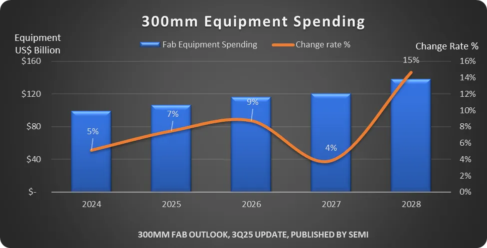
SEMICON West – PHOENIX — October 8, 2025 — Global 300mm fab equipment spending is expected to reach $374 billion from 2026 to 2028, SEMI reported today in its latest 300mm Fab Outlook. This robust investment reflects fab regionalization and surging AI chip demand for data centers and edge devices, while underscoring the growing commitment to semiconductor self-sufficiency across key regions through localized industrial ecosystems and supply chain restructuring.

SEMIWorldwide 300mm fab equipment spending is expected to surpass $100 billion for the first time in 2025, growing 7% to $107 billion. The report projects investment will increase 9% to $116 billion in 2026, 4% to $120 billion in 2027, and 15% to $138 billion in 2028.

“The semiconductor industry is entering a pivotal era of transformation, driven by unprecedented demand for AI-enabled technologies and a renewed focus on regional self-sufficiency,” said Ajit Manocha, President and CEO of SEMI. “Strategic global investments and collaboration are driving robust, advanced supply chains and faster deployment of next-generation semiconductor manufacturing technologies. The global expansion of 300mm fabs will enable progress in data centers, edge devices, and the digital economy.”


Segment Growth

The Logic & Micro segment is projected to lead equipment expansion with $175 billion in total investments from 2026 to 2028. Foundries are expected to be the primary drivers of this growth, fueled by sub-2nm capacity build-outs. Key enablers include advanced technologies such as gate-all-around (GAA) architecture and backside power delivery, which are essential to enhancing chip performance and power efficiency for increasingly demanding AI workloads. More advanced 1.4nm process technology is expected to enter volume production by 2028-2029. Additionally, AI performance improvements are anticipated to drive massive growth in edge-devices including automotive electronics, IoT applications, and robotics. Beyond advanced processes, demand across all nodes and various electronics devices is expected to surge significantly, fueling mature process equipment investment.

The Memory segment is projected to rank second with $136 billion in spending over the three-year period, marking the beginning of a new growth cycle for the segment. DRAM-related equipment investment is expected to exceed $79 billion from 2026 to 2028, with 3D NAND investment reaching $56 billion over the same period. AI training and inference have driven comprehensive demand increases across various types of memory. AI training requires greater data transmission bandwidth and extremely low latency, significantly boosting high bandwidth memory (HBM) demand. Moreover, model inference generates higher quality and more diverse AI digital content, creating substantial demand for end storage capacity and driving 3D NAND Flash requirements. This robust demand has sustained elevated levels of supply chain investment in memory over the medium to long term, helping to mitigate potential downturns from traditional memory cycle fluctuations.

Analog-related segments’ anticipated investment is projected to exceed $41 billion over the next three years.

Including Compound semiconductors, the power-related segment is expected to invest $27 billion from 2026 to 2028.

Regional Growth

China is expected to continue to lead in 300mm equipment spending with $94 billion in projected investments from 2026 to 2028, sustained by national self-sufficiency policies. 

Korea is projected to rank second in global 300mm equipment spending over the three-year period with $86 billion invested, supporting industries worldwide in generative AI demand. 

Taiwan is expected to invest $75 billion in 300mm equipment over the three years, ranking third. Investment will concentrate primarily on 2nm and sub-2nm capacity to maintain dominance in advanced foundry capacity and technology leadership.

The report projects Americas to invest $60 billion from 2026 to 2028, rising to fourth position. U.S. suppliers are expanding advanced process capacity to meet surging AI application demands while catalyzing domestic industrial and investment upgrades to maintain global technology development leadership.

Japan, Europe & Middle East, and Southeast Asia are projected to invest $32 billion, $14 billion, and $12 billion, respectively, over the three-year period. Policy incentives aimed at alleviating critical semiconductor supply concerns are expected to increase equipment investment by more than 60% in these regions by 2028 compared to 2024.

Part of the SEMI Fab Forecast database, the SEMI 300mm Fab Outlook lists 391 facilities and lines globally. The report reflects 173 updates and nine new fabs/lines projects since its last publication in January 2025.

For more information on the report or to subscribe to SEMI market data, visit SEMI Market Data or contact the SEMI Market Intelligence Team (MIT) at [email protected].

About SEMI

SEMI® is the global industry association connecting over 3,000 member companies and 1.5 million professionals worldwide across the semiconductor and electronics design and manufacturing supply chain. We accelerate member collaboration on solutions to top industry challenges through Advocacy, Workforce Development, Sustainability, Supply Chain Management and other programs. Our SEMICON® expositions and events, technology communities, standards and market intelligence help advance our members’ business growth and innovations in design, devices, equipment, materials, services and software, enabling smarter, faster, more secure electronics. Visit www.semi.org, contact a regional office, and connect with SEMI on LinkedIn and X to learn more.


Phoenix, Ariz. – October 8, 2025 – SEMI, the industry association serving the global semiconductor and electronics design and manufacturing supply chain, today announced Erich Thallner, President and Co-founder of EV Group (EVG), as its first SEMI Americas Catalyst Award recipient at SEMICON West 2025. This new award will be presented annually to individuals and organizations whose visionary leadership, technical excellence, and collaborative nature have uplifted the semiconductor industry. 

SEMISince founding EVG in 1980, Thallner has been instrumental in perfecting the company’s tight product development process, resulting in numerous innovations that have transformed the global industry. His consistent and strategic R&D investments have also positioned the company to quickly transition products from development and small-scale manufacturing to high-volume production. 

“Several important technologies would not have been realized without Erich's forward-thinking leadership,” said Joe Stockunas, President of SEMI Americas. “In an industry that constantly requires new innovations to keep up with rising chip demand, Erich’s commitment and ability to spot trends early have been fundamental for industry-wide advancement. SEMI is proud to honor Erich as our first SEMI Americas Catalyst Award recipient – his 45 years of dedicated industry service have set the bar high.” 

Thallner Thallner has led EVG to multiple groundbreaking and original discoveries, including the first double-sided mask aligner for MEMS commercialization, the first temporary bonding and debonding solution, and the first automated wafer bonding system for 300-mm wafers, among several others. 

Additionally, Thallner played a pivotal role in establishing EVG’s presence in the United States. Headquartered in St. Florian am Inn, Austria, the company brought its sales, technical equipment support, and process services to Arizona in 1994, decades before most others would follow suit. EVG has since expanded its North American presence to both Oregon and New Mexico and aligned with Arizona State University to support its Flexible Electronics and Display Center (FEDC). 

“I am deeply honored to accept the SEMI Americas Catalyst Award,” said Erich Thallner. “As a long-standing SEMI member, EVG shares the goals of this leading industry association to help the semiconductor supply chain members grow their business and address top challenges worldwide. In line with our Triple-i philosophy of ‘invent - innovate – implement’, we enable our customers, including our strategic partners in North America, to successfully realize their product ideas. Our North America subsidiary has played a pivotal role in this effort for more than 30 years.”

About SEMI

SEMI® is the global industry association connecting over 3,000 member companies and 1.5 million professionals worldwide across the semiconductor and electronics design and manufacturing supply chain. We accelerate member collaboration on solutions to top industry challenges through Advocacy, Workforce Development, Sustainability, Supply Chain Management and other programs. Our SEMICON® expositions and events, technology communities, standards and market intelligence help advance our members’ business growth and innovations in design, devices, equipment, materials, services and software, enabling smarter, faster, more secure electronics. Visit www.semi.org, contact a regional office, and connect with SEMI on LinkedIn and X to learn more. 


SEMICON West – PHOENIX – October 7, 2025 – SEMI and Semiconductor Digest today announced finalists for the Best of West award to be presented at SEMICON West 2025, October 7-9 at the Phoenix Convention Center (PCC) in Phoenix, Arizona. The Best of West Award winner will be announced at SEMICON West 2025 on Thursday, October 9 at 1 p.m. MST at the Smart Mobility/Smart MedTech Theater in the North Building, Level 300 of the PCC.

SEMICON WestPresented by SEMI Americas and Semiconductor Digest each year, the Best of West award recognizes innovative new products or services that are significantly advancing the electronics manufacturing supply chain or a particular manufacturing capability. 

The following Best of West 2025 finalists will showcase their products on the SEMICON West 2025 show floor:

Qnity, DuPont Electronics: Kalrez® 9400 – Booth 961

Kalrez® 9400 from DuPont™ is a next-generation perfluoroelastomer (FFKM) sealing solution specifically designed to meet the demanding requirements of advanced dry strip and etch processes in semiconductor manufacturing. As plasma chemistries evolve to include higher concentrations of reactive oxygen and hydrogen radicals, traditional sealing materials face accelerated erosion, particle generation, and reduced service life. Kalrez® 9400 addresses these challenges with a unique formulation that balances low erosion rates, minimal particle shedding, and superior thermal and mechanical stability.

Malema, Part of PSG, a Dover Company: LFC-7650 Series Ultrasonic Flow Controller – Booth 665

The Malema LFC-7650 Series Ultrasonic Flow Controller with integrated pressure transducer and state-of-the-art control algorithm provides ±1% metering accuracy with superior performance and repeatable control in all operating conditions. Offering a wide range of flow control from 504,000 mL/min, these closed-loop flow control modules are ideal for wet clean tools and post-CMP cleaning applications. 

Teradyne, Inc.: Magnum 7H – Booth 5645

With the proliferation of AI, high bandwidth memory (HBM) has become an integral part of AI processors due to its ability to handle the massive data processing and complex computations required by modern AI models. Teradyne Magnum 7H, a next-generation memory tester, is designed to meet the rigorous demands of testing HBM devices, integrated with GPUs and accelerators in high-performance, generative AI servers.

About Semiconductor Digest

Through a mix of news, contributed articles and staff-written articles, Semiconductor Digest (www.semiconductor-digest.com), is dedicated to providing global information about the design, manufacturing, packaging and testing of semiconductors and other types of electronic devices, including MEMs, LEDs, displays, power electronics, optoelectronics/photonics, biomedical devices, solar cells, thin film batteries and flexible electronics. Semiconductor Digest consists of a website, magazine and topic-focused newsletters.

About SEMI

SEMI® is the global industry association connecting over 3,000 member companies and 1.5 million professionals worldwide across the semiconductor and electronics design and manufacturing supply chain. We accelerate member collaboration on solutions to top industry challenges through Advocacy, Workforce Development, Sustainability, Supply Chain Management and other programs. Our SEMICON® expositions and events, technology communities, standards and market intelligence help advance our members’ business growth and innovations in design, devices, equipment, materials, services and software, enabling smarter, faster, more secure electronics. Visit www.semi.org, contact a regional office, and connect with SEMI on LinkedIn and X to learn more.


MUNICH, Germany — October 3, 2025 — Semiconductor industry experts will convene at SEMICON Europa 2025, November 18-21 at Messe München in Munich, to explore the latest trends and innovations in advanced packaging and fab management. The Advanced Packaging Conference (APC), Fab Management Forum (FMF) and MEMS and Imaging Sensors Summit (MEMS) at SEMICON Europa will each focus on driving sustainable solutions to meet the evolving demands of the semiconductor market. Co-located with productronica, SEMICON Europa is the region’s premier event connecting the entire electronics design and manufacturing supply chain. Registration is open for APC, FMF, and MEMS. 

SEMICON Europa“Global collaboration is of strategic importance to advancing Europe’s economic resilience and competitiveness,” said Laith Altimime, President of SEMI Europe. “The Advanced Packaging Conference, Fab Management Forum, and MEMS and Imaging Sensors Summit provide critical platforms for bringing together industry experts, innovators, and decision makers to ensure continued and sustainable growth throughout the European microelectronics supply chain.”

“We are entering a pivotal era where AI demands a radical rethinking of hardware innovation. At imec, we believe Europe’s strength lies in its ability to align research, industry, and policy around shared semiconductor roadmaps,” said Luc Van den hove, President and CEO of imec. “Our collaborative efforts, such as the NanoIC pilot line and our joint high NA EUV lithography research lab, demonstrate how collaboration can accelerate technology innovation to advance the development and adoption of next-generation technologies that impact industries on a broader scale. SEMICON Europa offers a unique opportunity to spotlight how collaborative innovation is shaping Europe’s semiconductor future—strengthening our competitiveness and reinforcing leadership across the entire value chain.”

Advanced Packaging Conference ─  
Advanced Packaging: Key Enabler for System Performance

The APC will spotlight innovations such as 2.5D and 3D stacking, chiplet integration, and heterogeneous packaging that are driving next-generation electronics. By improving power efficiency, thermal management, and system performance while enabling breakthroughs in high-performance computing and AI, advanced packaging is proving to be a critical enabler of superior performance, energy efficiency, and reliability.

This year’s APC will focus on:   

  • Market Insights in an Evolving Geopolitical Landscape
  • Advanced Materials and Processes for Wafer- and Panel-Level Packaging
  • Packaging Innovations for Silicon Photonics
  • Reliability and Yield Optimization with Digital Twin and AI
  • Advances in Testing, Inspection, and Metrology

Speakers include experts from 3D-Micromac AG, Advantest Europe, BESI Austria GmbH, Comet, Dassault Systèmes, DELO Industrial Adhesives, ESPAT-Consulting, Excillum AB, Fraunhofer IZM, GlobalFoundries, Henkel Electronic Materials, imec VZW, Lam Research, Lidrotec GmbH, NXP Semiconductors, Onto Innovation, RoodMicrotec GmbH, Shellback Semiconductor Equipment, and Siemens EDA.

The conference is sponsored by ASE, MKS | Atotech, Deaxo, Exyte, SUSS, Techno Horizon

Fab Management Forum ─  
Europe’s Fab Resilience Through Collaboration 

Collaborative innovation can strengthen Europe’s semiconductor manufacturing ecosystem. This year’s FMF will feature discussions on strategies to enhance fab efficiency and performance through cutting-edge technologies while maintaining sustainability. Attendees will gain insights into fostering partnerships that drive both competitiveness and long-term sustainability in semiconductor production.

FMF topics will focus on:  

  • Competitive Fab Strategies for Europe
  • Collaboration for European Supply Chain Resilience
  • Smart Factories Powered by Automation and AI
  • Disruptive Technologies Reshaping Fabs

Speakers include experts from ACCRETECH, Air Liquide, Bosch, Comet, Dorfner Anzaplan GmbH, Inficon, Infineon Technologies, Neura Robotics, Nippon Gases, Planimize, Semilab, SEMI, Siemens, STMicroelectronics, Swansea University, and X-Fab. 

The conference is sponsored by ACCRETECH, Anzaplan Dorfner Group, Comet, Deaxo, Exyte, INFICON, Planimize, Semilab, Spanish Society for Technological Transformation, Siemens, and VAT.

MEMS & Imaging Sensors Summit ─
Sensing (R)evolution: Sustaining Europe's Leadership

The summit will showcase how the latest MEMS and imaging technologies are enabling next-level value creation across industries. Explore cutting-edge AI-enhanced sensing, data fusion, and their transformative impact on automotive, healthcare, smart systems, and defence.

MEMS topics will focus on:  

  • Geopolitical Trends and Supply Chain Collaborations
  • Future and MEMS and Imaging Technologies
  • AI-Driven MEMS & Imaging Optimization
  • AR/VR: Technologies Driving Immersive Experiences
  • Breakthroughs in Advanced Sensor Technologies for Defence

Speakers include experts from Airbus DS, Bosch, CEA-Leti, Comet AG, EssilorLuxottica, EYE-TECH srl, Eyeo, Infineon, imec, NXP Semiconductors, Robert Bosch GmbH, SisuSemi Ltd, STMicroelectronics, VTT, X-Fab, Yole Group.

The conference is sponsored by ASE, Infineon, KLA, and STMicroelectronics.

We extend our gratitude to the Advanced Packaging Conference Committee, Fab Management Forum Committee, and MEMS & Imaging Sensors Committee members for their invaluable support in shaping an exceptional program.

To learn more about SEMICON 2025 program highlights, view our press release: SEMICON Europa 2025 Spotlights Global Collaborations for European Economic Resilience or visit the SEMICON Europa 2025 website. 

Programs in halls B1, C1, C2 and Entrance West are complimentary for all SEMICON Europa and productronica visitors. Press and media partners can register for free by contacting Sitong He at [email protected].

Connect with SEMI Europe on LinkedIn or YouTube @SEMIEurope (#SEMICONEuropa).

SEMICON Europa 2025 Sponsors

About SEMI 

SEMI® is the global industry association connecting over 3,000 member companies and 1.5 million professionals worldwide across the semiconductor and electronics design and manufacturing supply chain. We accelerate member collaboration on solutions to top industry challenges through Advocacy, Workforce Development, Sustainability, Supply Chain Management and other programs. Our SEMICON® expositions and events, technology communities, standards and market intelligence help advance our members’ business growth and innovations in design, devices, equipment, materials, services and software, enabling smarter, faster, more secure electronics. Visit www.semi.org, contact a regional office, and connect with SEMI on LinkedIn and X to learn more.  


Phoenix, Ariz. — October 7, 2025 — SEMI, the industry association serving the global semiconductor and electronics design and manufacturing supply chain, today announced Lam Research Corp. as the recipient of the 2025 SEMI Award for North America. Lam earned the recognition for its cryogenic etch technology, a breakthrough innovation that advances 3D NAND device manufacturing essential for today’s data-intensive AI applications. SEMI Americas presented the award to Lam during SEMICON® West, the premier microelectronics exhibition taking place in Phoenix, Arizona this week.

The rapid proliferation of generative and on-device AI is driving exponential demand for high-capacity, high-performance memory solutions. 3D NAND has become the standard architecture for flash memory, with companies working to stack hundreds of layers to boost density and performance. Achieving this requires advanced etching technologies that enable precise, deep, and repeatable etching, critical for supporting the industry’s roadmap toward 1,000-layer devices by 2030.

“The SEMI Award for North America has recognized outstanding innovations in the semiconductor industry for over 45 years,” said Joe Stockunas, president, SEMI Americas. 

“We are proud to recognize Lam, whose pioneering cryogenic etch technology not only showcases the company’s legacy of etch innovation, but also its leadership in 3D NAND dielectric etch technology to accelerate innovation that drives our industry forward.” 

Cryogenic etch technology operates at low temperatures, enabling the use of novel chemistries that significantly advance high aspect ratio etching. Lam’s third generation, production proven cryogenic etch technology, Lam Cryo™ 3.0 is a breakthrough innovation delivering enhanced etch rates, highly vertical profiles, and improved process control critical for fabricating complex 3D NAND structures and improving scalability. In addition to its performance benefits, Lam Cryo 3.0 offers 40% reduction in energy consumption per wafer, and up to a 90% reduction in emissions compared to conventional etch processes.*

"As the industry strives to make memory smaller and taller, Lam Cryo 3.0 technology overcomes key scaling obstacles to pave the way for 1,000-layer 3D NAND," said Tae Won Kim, corporate vice president of dielectric etch at Lam Research. "We proudly thank SEMI for this recognition, as well as our incredibly talented development teams around the world whose innovations across plasma reactors, processes and chemistry have enabled the production of millions of leading-edge wafers NAND wafers on Lam cryogenic etch technologies.”

The highest honor conferred by the SEMI Americas region, the SEMI Award was established in 1979 to recognize outstanding technical achievement and commendable contributions by individuals and teams in the areas of Semiconductor Materials, Wafer Fabrication, Assembly and Packaging, Process Control, Test and Inspection, Robotics and Automation, Quality Enhancement, and Process Integration.

Nominations are open to individuals or teams from industry and academia whose accomplishments have a broad commercial impact and technical significance for the semiconductor industry. SEMI invites 2026 SEMI Award for North America nominations from individuals or teams with North American-based SEMI member companies. See the list of past award recipients.

Learn more about SEMICON West 2025. SEMICON West 2026 will be held in October in San Francisco and will return to Phoenix in 2027, alternating years between the two locations.

* Source: Lam Research. Based on new etch chemistries possible with Lam Cryo 3.0. 90% reduction in Kg CO2 per wafer. Estimated emissions reduction calculated using IPPC (Intergovernmental Panel on Climate Change) guidelines for greenhouse gas inventories. The estimated reduction has not been independently verified.

About SEMI

SEMI® is the global industry association connecting over 3,000 member companies and 1.5 million professionals worldwide across the semiconductor and electronics design and manufacturing supply chain. We accelerate member collaboration on solutions to top industry challenges through Advocacy, Workforce Development, Sustainability, Supply Chain Management and other programs. Our SEMICON® expositions and events, technology communities, standards and market intelligence help advance our members’ business growth and innovations in design, devices, equipment, materials, services and software, enabling smarter, faster, more secure electronics. Visit www.semi.org, contact a regional office, and connect with SEMI on LinkedIn and X to learn more. 


MILPITAS, Calif. — October 6, 2025 — Electronic System Design (ESD) industry revenue increased 8.6% to $5,089.4 million in the second quarter of 2025 from the $4,685.5 million registered in the second quarter of 2024, the ESD Alliance, a SEMI Technology Community, announced today in its latest Electronic Design Market Data (EDMD) report. The four-quarter moving average rose 10.4%, based on a comparison of the most recent four quarters to the prior four.

SEMI ESDA“The electronic design automation (EDA) industry continues to report strong year-over-year revenue growth in Q2 2025,” said Walden C. Rhines, Executive Sponsor of the SEMI Electronic Design Market Data report. “Product categories including Computer-Aided Engineering (CAE), Printed Circuit Board and Multi-Chip Module, Semiconductor IP, and Services reported increases, with CAE and Services showing double digit gains. Geographic regions including Americas, EMEA, and APAC reported growth in Q2, even hitting double digits in Americas and EMEA.”

The companies tracked in the EDMD report employed 72,529 people globally in Q2 2025, a 14.8% increase over the Q2 2024 headcount of 63,188 and up 12.6% compared to Q1 2025. 

The quarterly EDMD report contains detailed revenue information within the following category and geographic breakdowns. 

Revenue by Product and Application Category – Year-Over-Year Change

  • Computer-Aided Engineering (CAE) revenue increased 17.2% to $1,929 million. The four-quarter CAE moving average increased 13.5%.
  • IC Physical Design and Verification revenue decreased 9.9% to $701.9 million. The four-quarter moving average for the category decreased 3.1%.
  • Printed Circuit Board and Multi-Chip Module (PCB and MCM) revenue rose 7.8% to $430.5 million. The four-quarter moving average for PCB and MCM rose 8.8%.
  • Semiconductor Intellectual Property (SIP) revenue increased 8.7% to $1,826.7 million. The four-quarter SIP moving average rose 13.2%.
  • Services revenue increased 11.9% to $201.2 million. The four-quarter Services moving average rose 21.3%.

Revenue by Region – Year-Over-Year Change

  • The Americas, the largest reporting region by revenue, procured $2,282.4 million of electronic system design products and services in Q2 2025, a 12.2% increase. The four-quarter moving average for the Americas rose 14.1%.
  • Europe, Middle East, and Africa(EMEA) procured $650.9 million of electronic system design products and services in Q2 2025, an 11.4% increase. The four-quarter moving average for EMEA grew 10.7%.
  • Japan’s procurement of electronic system design products and services decreased 9.2% to $277.4 million. The four-quarter moving average for Japan increased 4.4%.
  • Asia Pacific (APAC) procured $1,878.7 million of electronic system design products and services in Q2 2025, a 6.7% increase. The four-quarter moving average for APAC grew 7.2%. 

About the EDMD Report

The ESD Alliance Electronic Design Market Data (formerly the Market Statistics Service) report presents Electronic Design Automation (EDA), SIP and Services industry revenue data quarterly. Both public and private companies contribute data to the report available from SEMI. Each quarterly report is published approximately three months after quarter close. EDMD report data is segmented as follows: 

  • Revenue by product category (CAE, IC Physical Design and Verification, SIP, PCB/MCM Layout, and Services) including numerous detailed sub-categories
  • Revenue by geographic region (Americas, EMEA, Japan and APAC)
  • Total employment at participating companies

For information about SEMI market research reports, visit the SEMI Market Research Reports and Databases Catalog.

About the Electronic System Design Alliance

The Electronic System Design (ESD) Alliance, a SEMI Technology Community, is the central voice to communicate and promote the value of the semiconductor design ecosystem as a vital component of the global electronics industry. As an international association of companies providing goods and services throughout the semiconductor design ecosystem, it is a forum to address technical, marketing, economic and legislative issues affecting the entire industry. For more information about the ESD Alliance, visit http://esd-alliance.org.

Follow the ESD Alliance

About SEMI

SEMI® is the global industry association connecting over 3,000 member companies and 1.5 million professionals worldwide across the semiconductor and electronics design and manufacturing supply chain. We accelerate member collaboration on solutions to top industry challenges through Advocacy, Workforce Development, Sustainability, Supply Chain Management and other programs. Our SEMICON® expositions and events, technology communities, standards and market intelligence help advance our members’ business growth and innovations in design, devices, equipment, materials, services and software, enabling smarter, faster, more secure electronics. Visit www.semi.org, contact a regional office, and connect with SEMI on LinkedIn and X to learn more.

The information supplied by the ESD Alliance is believed to be accurate and reliable, but the ESD Alliance assumes no responsibility for any errors that may appear in this document. All trademarks and registered trademarks are the property of their respective owners.


MILPITAS, Calif. — Oct. 2, 2025 — SEMI, the industry association serving the global semiconductor and electronics design and manufacturing supply chain, today announced Greg Barrett as its new Chief Financial and Business Operations Officer. Barrett brings more than 30 years of industry expertise to his role, in which he will work to create measurable value for SEMI members and lead the organization’s financial profitability and operational strategies.

SEMI“Greg’s specialized industry expertise will be beneficial for helping SEMI reach its financial, operational, and membership goals,” said Ajit Manocha, SEMI President and CEO. “His excellence in strategic planning and corporate finance for the semiconductor industry aligns with our mission to foster growth and innovation across the global microelectronics ecosystem. We’re confident that Greg will make an outstanding addition to our global leadership team.”

Before joining SEMI, Barrett served as Senior Vice President and CFO of Efinix, a programmable semiconductor company. He also held senior-level finance roles at Super Micro Computer, Rambus, Micron Technology, and Altera. 

“I’m honored to join SEMI as its Chief Financial and Business Operations Officer,” said Barrett. “As semiconductor technologies become more complex, the need for unified industry engagement becomes more apparent. I look forward to advancing this mission alongside SEMI’s senior leaders and board members.”

Barrett succeeds former SEMI CFO and Business Operations officer, Kevin Bauer.

“Kevin was instrumental in laying a strong foundation for SEMI’s financial growth strategy,” said Manocha. “He guided SEMI in financing the expansion of our programs to address the global semiconductor industry’s most pressing challenges, and he executed on our strategic plan to develop diversified revenue streams and emerge stronger than ever post-pandemic. We thank Kevin for his invaluable service to SEMI, our members and the industry.”

Barrett earned his master’s degree in business administration from Santa Clara University and his bachelor’s degree in finance from California State University of Chico. He will report directly to Manocha.

About SEMI

SEMI® is the global industry association connecting over 3,000 member companies and 1.5 million professionals worldwide across the semiconductor and electronics design and manufacturing supply chain. We accelerate member collaboration on solutions to top industry challenges through Advocacy, Workforce Development, Sustainability, Supply Chain Management and other programs. Our SEMICON® expositions and events, technology communities, standards and market intelligence help advance our members’ business growth and innovations in design, devices, equipment, materials, services and software, enabling smarter, faster, more secure electronics. Visit www.semi.org, contact a regional office, and connect with SEMI on LinkedIn and X to learn more. 


Brussels, Belgium - September 30, 2025 - SEMI Europe, along with over 75 semiconductor and microelectronics companies, research and technology organizations (RTOs) and trade associations, officially endorse the Declaration of the Semicon Coalition. Signed by all 27 European Union (EU) Member States, the declaration calls for a revised EU Chips Act to strengthen and revitalize Europe's position in the global semiconductor industry.

SEMI Europe welcomes the Council Members' initiative to enhance the current chips framework in Europe to create the appropriate pre-conditions for the semiconductor industry in Europe to strive to achieve its goals. These pre-conditions must favour cross-segment synergies between RTOs and the industry, including small and medium-sized business (SMEs) and startups, while guaranteeing the industrial uptake of pilot lines' R&D outputs and a widened policy toolbox to support the industry's deployment in Europe.

“Building a European ecosystem for semiconductors requires a holistic approach, encompassing synergies with strategic policy initiatives, including economic security, AI and quantum,” said Laith Altimime, President, SEMI Europe. “The EU must set a secured budget line for semiconductors in the next Multiannual Financial Framework (MFF) with simplified procedures and revised competition rules for the industrial uptake of R&D outputs.”

With this joint endorsement, the European semiconductor industry should demonstrate its full support to make semiconductors a highly strategic priority for Europe. SEMI Europe and the letter's signatories call on the European Commission to design an ambitious Chips Act 2.0, which will deliver on regulatory and administrative simplification, incentive programs, faster permitting, grid access, power supply, stable supporting infrastructure, access to talent and secured access to critical raw materials.

Developing a market-driven business case that connects European and global markets while facilitating international partnerships will be key to achieving the EU's strategic objectives.

SEMI Europe Advocacy

Discover how SEMI Europe Advocacy & Public Policy supports the microelectronics industry across sustainability, trade, talent, and R&D, or become involved by contacting [email protected]. 

About SEMI

SEMI® is the global industry association connecting over 3,500 member companies and 1.5 million professionals worldwide across the semiconductor and electronics design and manufacturing supply chain. We accelerate member collaboration on solutions to top industry challenges through Advocacy, Workforce Development, Sustainability, Supply Chain Management, and other programs. Our SEMICON® expositions and events, technology communities, standards, and market intelligence help advance our members’ business growth and innovations in design, devices, equipment, materials, services, and software, enabling smarter, faster, more secure electronics. Visit www.semi.org, contact a regional office, and connect with SEMI on LinkedIn and X to learn more.