
58 Partners Charged with Implementing Cutting-Edge Solutions for Emission Control, Materials Innovation, Waste Reduction, and Raw Material Reuse
Brussels, Belgium – June 19, 2025 – A pan-European consortium dedicated to developing sustainable processes and technologies for the semiconductor manufacturing industry today announced the launch of the GENESIS project. This integrated, large-scale initiative aims to enable Europe’s chip industry to meet its sustainability goals—from materials development to final waste treatment.
Coordinated by CEA-Leti, the three-year project brings together 58 partners spanning the entire European semiconductor value chain, from large enterprises and subject matter experts (SMEs) to research institutes, universities, and industry associations. GENESIS will drive innovative solutions in emission control, eco-friendly materials such as alternatives to per- and polyfluoroalkyl substances (PFAS), waste minimization, and raw material reuse, directly aligned with the European Green Deal and European Chips Act.
“GENESIS partners are committed to fruitful and constructive collaboration throughout the duration of the project to deliver lasting impact on the European semiconductor ecosystem,” said Laurent Pain, Sustainable Electronics Program Director at CEA-LETI, and Coordinator of the GENESIS project.
SEMI Europe will oversee the dissemination of communication and promotion of activities to raise awareness and understanding of the importance of sustainable semiconductor manufacturing technologies across both industry and academia.
 “The European semiconductor industry recognizes the urgency of seeking alternatives to substances of high concern, and reducing greenhouse gas emissions,” said Laith Altimime, President of SEMI Europe. “With semiconductor demand rising, the European Commission's funding of crucial initiatives such as GENESIS drives sustainable innovative solutions.”
The GENESIS consortium will focus on scientific research to facilitate the industry's transition toward sustainable manufacturing throughout the project’s three-year term. Additionally, the initiative will deliver added value through knowledge sharing, job creation, and positive socioeconomic impacts across the European regions represented by project partners.
45 Sustainability Innovations Driven by Four Strategic Pillars
Pain noted that the GENESIS project team expects to deliver approximately 45 sustainability-driven innovations covering the semiconductor lifecycle, guided by four strategic pillars that form the technological foundation of GENESIS’s vision for a green European semiconductor industry:
- Pillar 1 – Monitoring & Sensing: Real-time emissions tracking, traceability, and process feedback systems,
- Pillar 2 – New Materials: PFAS-free chemistries and low-GWP alternatives for advanced semiconductor processes,
- Pillar 3 – Waste Minimization: Innovations in recycling (solvent, gas, slurries), reuse, and sustainable replacements, and
- Pillar 4 – Critical Raw Materials Mitigation: Strategies to reduce dependency on CRM and strengthen resource security.
Complimenting these pillars, the project’s objectives establish an overall framework that includes deploying sensor-integrated abatement systems to reduce PFAS and greenhouse gas emissions. It also aims to position Europe as a leader in green semiconductor innovation by aligning supply-chain practices with environmental regulations.
A Green Fit for Europe’s Chips Agenda
“The launch of the GENESIS project marks a critical step toward aligning Europe’s semiconductor ambitions with its climate commitments,” said Anton Chichkov, head of programs at Chips Joint Undertaking (Chips JU), a public-private partnership created to bolster Europe's semiconductor industry by fostering collaboration between the EU, member states, and the private sector.
“As chips become the backbone of everything from AI to energy systems, their environmental footprint is rapidly growing,” said Chichkov. “GENESIS responds to this urgent challenge by pioneering sustainable alternatives in materials, waste reduction, and resource efficiency. Through this initiative, Europe is not only investing in cleaner technologies—it’s positioning itself as a global leader in green semiconductor manufacturing.”
With a budget of close to €55 million, the GENESIS project is co-funded through the Chips Joint Undertaking by the European Commission, participating EU member states, and the Swiss State Secretariat for Education, Research and Innovation (SERI).
The Five Critical Stages in Chip-Making Lifecycle Addressed by GENESIS
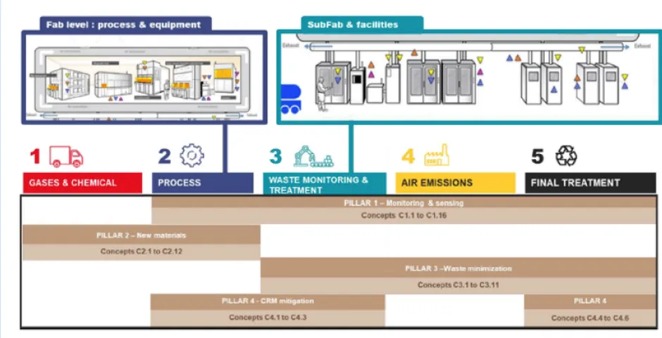
The GENESIS integrated roadmap outlines five critical stages in the semiconductor manufacturing lifecycle—materials (PFAS-free alternatives & gases and chemicals, processes, waste monitoring & treatments, air emissions, and final treatments—where environmental impact can be minimized.
This structured approach guides the project’s efforts to reduce emissions, eliminate harmful substances, and enable material recovery through innovation in sensing, materials, waste reduction, and raw material reuse.
About GENESIS
GENESIS (GENErate a Sustainable Industry for Semiconductors) is a pan-European project co-funded by the EU, Chips JU, Member States, and the Swiss State Secretariat for Education, Research and Innovation (SERI). Coordinated by CEA-Leti, it includes 58 partners from across Europe, focused on leading semiconductor manufacturing into a circular economy model, which aims to minimize waste and maximize resource reuse, and a low-impact, innovation-driven industry. https://www.genesiseu.eu/
About SEMI
SEMI® is the global industry association connecting over 3,000 member companies and 1.5 million professionals worldwide across the semiconductor and electronics design and manufacturing supply chain. We accelerate member collaboration on solutions to top industry challenges through Advocacy, Workforce Development, Sustainability, Supply Chain Management, and other programs. Our SEMICON® expositions and events, technology communities, standards, and market intelligence help advance our members’ business growth and innovations in design, devices, equipment, materials, services, and software, enabling smarter, faster, more secure electronics. Visit www.semi.org, contact a regional office, and connect with SEMI on LinkedIn and X to learn more.
Association Contacts
Jatin Mendiratta / SEMI Europe
Phone: +49 160 402 8899
Email: [email protected]
Samer Bahou / SEMI Corporate
Phone: +1 408 943 7870
Email: [email protected]


