
downloadGroupGroupnoun_press release_995423_000000 copyGroupnoun_Feed_96767_000000Group 19noun_pictures_1817522_000000Member company iconResource item iconStore item iconGroup 19Group 19noun_Photo_2085192_000000 Copynoun_presentation_2096081_000000Group 19Group Copy 7noun_webinar_692730_000000Path
Skip to main content
Default Banner Image

SEMI Press Release

ID
semi-press-release

KUALA LUMPUR, Malaysia – April 21, 2026 – SEMICON Southeast Asia (SEMICON SEA) 2026, the region’s premier platform for the global semiconductor and electronics manufacturing supply chain, will return to the Malaysia International Trade and Exhibition Centre (MITEC) in Kuala Lumpur from 5 to 7 May. Registration is open.

The event underscores the region’s growing strategic importance in the global semiconductor ecosystem, as Southeast Asia continues to strengthen its role across advanced manufacturing and supply chain resilience. In Malaysia, the event, held in strategic partnership with the Ministry of Investment, Trade and Industry (MITI) and the Malaysian Investment Development Authority (MIDA), reflects the country’s continued push to strengthen its position in the global semiconductor ecosystem.

SEMICON SEA 2026 will be themed Transform Tomorrow and will focus on accelerating next-generation technologies while addressing current structural challenges. It is expected to bring together more than 20,000 innovators, policymakers, and technology experts, fostering collaboration across the international semiconductor value chain, and provide the latest insights on artificial intelligence, smart manufacturing, sustainability, workforce development, advanced packaging, supplier sourcing, and more.

The global semiconductor industry is expected to reach USD1 Trillion in annual sales in 2026, a historic milestone fuelled by an intensifying AI infrastructure boom. Market analysts note that Southeast Asia has emerged as a significant driver of global semiconductor growth, having outperformed the broader industry over the past few years, supported by sustained expansion in manufacturing capacity, assembly, testing and packaging, as well as its increasing integration into global semiconductor supply chains.

“The semiconductor industry is entering a new era where progress will be defined by effective collaboration across the entire ecosystem,” said Ajit Manocha, President and CEO, SEMI. “SEMICON Southeast Asia reflects this changing landscape through its programs focused on closing gaps between innovation and execution – from design all the way to manufacturing. SEMI looks forward to hosting this year’s event in Malaysia, a semiconductor industry powerhouse with decades of proven success.” 

“SEMICON Southeast Asia is a catalyst for driving collaboration and innovation across the semiconductor ecosystem, bringing together leaders, visionaries, and experts to address the industry’s most pressing challenges and seize emerging opportunities,” said Linda Tan, President, SEMI Southeast Asia. “As advanced technologies reshape manufacturing, SEMICON Southeast Asia empowers stakeholders to connect, exchange knowledge, and shape the future of the industry.”

Closer to home, Malaysia’s semiconductor industry is entering its next phase of growth from a position of strength. The electrical and electronics (E&E) sector secured RM28.5 billion in approved investments in 2025, reaffirming its role as a cornerstone of Malaysia’s manufacturing economy and a trusted node in the global technology supply chain. SEMICON Southeast Asia 2026 arrives at a moment when Malaysia is moving beyond its established strengths in assembly and test into higher-value activities, including design, advanced packaging, and innovation-driven manufacturing.

“The semiconductor industry is at an inflection point, and Malaysia intends to be at the center of what comes next,” said Datuk Sikh Shamsul Ibrahim Sikh Abdul Majid, Chief Executive Officer of MIDA. “Under the New Industrial Master Plan (NIMP) 2030, Malaysia is not simply maintaining its position in the global semiconductor supply chain. We are deliberately reshaping it. Our investment fundamentals are strong. The RM28.5 billion secured by the E&E sector in 2025 is proof that global confidence in Malaysia has not wavered. We continue to build its robust ecosystem to match that confidence, through supply chain integration, local capability development, and the kind of high-value partnerships that platforms like SEMICON Southeast Asia are uniquely placed to catalyze. MIDA’s role here is not as a bystander. We are an active builder of his industry’s next chapter in Malaysia, and we are here to build it together.”

SEMICON SEA 2026 Focus Areas 

  • AI and Intelligent Manufacturing: Dedicated AI forums and the new Intelligent Manufacturing Showcase developments in advanced manufacturing capabilities across the semiconductor ecosystem, including smart manufacturing, automation, digitalisation, and sustainability. This also supports talent development by exposing engineers and students to real‑world AI applications and future‑ready manufacturing roles.
  • Sustainability: Three days of dedicated sustainability discussions and a new Sustainability Pavilion focusing on energy, emissions, and efficiency, underscoring the semiconductor industry’s growing need to address global energy pressures while advancing a more sustainable growth pathway.
  • Talent Development: Workforce development in action through TECH Zoomers Bootcamp, TalentCONNECT, mentoring sessions, curated tours and career-focused programs, aligned with Malaysia’s National Semiconductor Strategy, which aims to train and upskill 60,000 highly skilled engineers by 2030. SEMICON Southeast Asia 2026 serves as a key platform to support this ambition by strengthening industry exposure, talent pipelines and skills development across the semiconductor ecosystem.
  • Advanced Packaging & Heterogeneous Integration: One and a half days of expert-led discussions on advanced packaging and heterogeneous integration, underscoring their importance in enabling next-generation semiconductor innovation and accelerating the industry’s move toward higher value creation across the value chain.
  • Suppliers Sourcing Programme: Targeted business matching featuring five leading global buyer companies engaging in pre-scheduled one-to-one meetings with suppliers to explore sourcing opportunities and new partnerships, serving as a strategic platform to deepen ecosystem linkages across the region.

MIDA Initiatives at SEMICON SEA 2026

At SEMICON SEA 2026, MIDA is running three program tracks that go beyond conversation to drive tangible outcomes for Malaysia’s semiconductor ecosystem:

  • The Supply Chain Integration & Capability Enhancement Forum brings together global semiconductor companies, Malaysian suppliers, and ecosystem stakeholders to share insights on industry trends, supplier expectations, and capability development. It aims to strengthen Malaysia’s supply chain ecosystem and support its advancement into higher-value segments of the semiconductor value chain.
  • The Digital Twin & Smart Manufacturing Seminar is aimed at Malaysian small and medium enterprises (SMEs) in the semiconductor and mobility supply chains, focusing on the practical adoption of digital twin technology and smart manufacturing. The goal is direct: raise the capabilities of local suppliers so they can meet the standards and requirements of global manufacturers operating in Malaysia.
  • The Handshake@SEMICON convenes senior decision-makers from leading global semiconductor and technology companies into direct, structured engagements. MIDA facilitates these engagements with a clear intent: to move from interest to investment, and from introduction to partnership.
  • Through SEMI’s TECH Zoomers programme at Universiti Kebangsaan Malaysia (UKM), MIDA will facilitate and contribute to a panel discussion on workforce development trends and job outlook in the semiconductor sector, to equip students and early talent with industry-relevant insights and strengthen Malaysia’s future semiconductor workforce.

SEMICON SEA is further strengthened by the support of leading partners and industry sponsors. 

  • Diamond Sponsors: GlobalFoundries, Lam Research, Micron, Sandisk Corporation, Tokyo Electron Limited
  • Platinum Sponsors: Applied Materials, Global TechSolutions, Schneider Electric, SGS, Soitec, STATS ChipPAC
  • Gold Sponsors: Advantest, ASE, ECOWorld, Henkel, IAQ, KLA, Kulicke & Soffa, Siemens, Singtest, STMicroelectronics 

Registration for SEMICON SEA 2026 is now open. For full program and conference details, please visit the SEMICON SEA website. 

About SEMI 

SEMI® is the global industry association connecting over 3,000 member companies and 1.5 million professionals worldwide across the semiconductor and electronics design and manufacturing supply chain. We accelerate member collaboration on solutions to top industry challenges through Advocacy, Workforce Development, Sustainability, Supply Chain Management and other programs. Our SEMICON® expositions and events, technology communities, standards and market intelligence help advance our members’ business growth and innovations in design, devices, equipment, materials, services and software, enabling smarter, faster, more secure electronics. Visit www.semi.org, contact a regional office, and connect with SEMI on LinkedIn and X to learn more.

About MIDA

MIDA is the government’s principal investment promotion and development agency under the Ministry of Investment, Trade and Industry (MITI) to oversee and drive investments into the manufacturing and services sectors in Malaysia. Headquartered in Kuala Lumpur Sentral, MIDA has 12 regional and 20 overseas offices. MIDA partners with investors at every stage of their journey, supporting sustainable growth and long-term value creation for Malaysia. For more information, please visit www.mida.gov.my and follow MIDA on X, Instagram, Facebook, LinkedIn, TikTok and YouTube.

MILPITAS, Calif. – April 27, 2026 – The second edition of SEMIEXPO Heartland opens this week, April 29-30 at the Detroit Marriot at the Renaissance Center in Detroit, Michigan, centered around smart manufacturing, automotive electronics, and workforce development. The exposition will bring together innovators, manufacturers, suppliers, and emerging talent from across the semiconductor and microelectronics ecosystem for two days of high-impact networking and industry insight. Registration is open.

semiexpo“SEMIEXPO Heartland will highlight smart mobility and smart manufacturing innovations – two critical end markets that play pivotal roles in the semiconductor industry’s path to $1 trillion,” said Joe Stockunas, President, SEMI Americas. “By bringing together the automotive and semiconductor ecosystems in Detroit—a hub for innovation, manufacturing and economic growth—we can collectively address industry challenges and accelerate the evolution toward software-defined, electrified, autonomous, and AI-enabled vehicles.”

Designed as a catalyst for collaboration, SEMIEXPO Heartland creates a dynamic environment where thought leaders, technology experts, and business decision-makers can engage in meaningful conversations about the future of the semiconductor supply chain. Attendees will experience a curated program featuring keynote presentations, technical sessions, and interactive panels that highlight the region’s rapidly expanding role in advanced manufacturing and chip innovation.

SEMIEXPO Heartland Conference Highlights

Keynote Speakers

  • The Honorable Gretchen Whitmer, Governor of Michigan
  • The Honorable Marek Laco, Deputy Assistant Secretary for the Employment and Training Administration, U.S. Department of Labor 
  • GM: Linda Cadwell Stancin, Executive Director and Head of Research & Development
  • KLA: John McLaughlin, Global ESG Leader & Ann Arbor Site Lead
  • KLA: Vijay Ramachandran, Director, AI and Modeling Center of Excellence
  • MIPS, A GlobalFoundries Company: Sameer Wasson, CEO 

SEMIEXPO Heartland will feature a focused exposition showcasing solution providers delivering the technologies, equipment, materials, and services driving smart manufacturing and smart mobility. The exhibits offer attendees a hands-on opportunity to explore real-world solutions, engage directly with technology experts, and identify partners addressing critical challenges across the semiconductor and microelectronics value chain from advanced manufacturing and automation to automotive electronics and workforce readiness.

Smart Manufacturing Sessions will focus on how digital twins are optimizing automotive manufacturing to realize the vision of lights-out factories, sensor-driven automation is transforming the shop floor, and the new wave of automotive chiplets and advanced packaging is revolutionizing vehicle electronics. Industry leaders in innovation and operations will share real-world case studies from the trenches—along with their vision for how physical AI and AI-driven processes will reshape automotive manufacturing. 

Smart Mobility Sessions will bring the automotive and semiconductor supply chains together with the goal to exchange perspectives on game-changing trends such as software-defined vehicles, self-driving cars, electrified mobility, and how all that is powered by cutting edge chip technologies, smart sensing systems, and artificial intelligence.

SEMI’s signature Workforce Development Pavilion will illuminate a different pathway to success. It is the perfect place to network with potential employers, discover job opportunities, learn about innovations in the industry, and navigate your career. 

View the full SEMIEXPO Heartland 2026 agenda for updates on speakers and to learn more. This year’s partners include the Michigan Economic Development Corporation (MEDC) and MSTAR. 

For press interested in attending SEMIEXPO Heartland 2026, please contact Sherrie Gutierrez at [email protected]. 

Follow SEMI 

About SEMI

SEMI® is the global industry association connecting over 4,000 companies and 1.5 million professionals worldwide across the semiconductor and electronics design and manufacturing supply chain. We accelerate member collaboration on solutions to top industry challenges through Advocacy, Workforce Development, Sustainability, Supply Chain Management and other programs. Our SEMICON® expositions and events, technology communities, standards and market intelligence help advance our members’ business growth and innovations in design, devices, equipment, materials, services and software, enabling smarter, faster, more secure electronics. Visit www.semi.org, contact a regional office, and connect with SEMI on LinkedIn and X to learn more.  


PHOENIX, Arizona – April 14, 2026 – The SEMI Foundation today announced the extension of SEMIquest, its immersive, hands-on STEM experience at Arizona Science Center through May 31, 2026. Originally launched in conjunction with SEMICON West 2025, the extended run will provide thousands more students, educators, and families with direct exposure to the semiconductor industry and the career pathways powering today’s technology-driven world.

This extension is made possible through the continued support of industry partners like TMSC, Amkor, Nikon, and ASM, reinforcing a shared commitment to strengthening Arizona’s and the nation’s microelectronics workforce pipeline.

SEMIquest is part of the SEMI Foundation’s broader effort to build a future-ready workforce for the semiconductor and microelectronics industry. Through initiatives such as the National Network for Microelectronics Education (NNME) and SEMI University (SEMI U), the Foundation is aligning education, workforce systems, and industry to create clear, scalable pathways into high-demand careers.

“Extending SEMIquest allows us to deepen our impact at a moment when awareness must translate into action,” said Perla DeBaggis, Sr. Specialist, Career & Industry Awareness Navigator at the SEMI Foundation. “Students are not just learning about semiconductors. They are seeing where they fit. This experience makes the industry more real, accessible, and within reach, and that is how we begin to build the workforce of the future.”

Expanding Access to High-Impact STEM Experiences

Since its debut in October 2025, SEMIquest has served as a dynamic entry point for more than 80,000 visitors, giving them a glimpse into the world of semiconductors through interactive, career-connected learning experiences designed to move students from curiosity to exploration. With the extension through May 31, even more visitors will have the opportunity to engage with:

  • A pop-up exhibition showcasing real-world semiconductor applications
  • Hands-on STEM activities
  • “Day in the Life” insights from industry professionals
  • Career pathway exploration tied to real jobs in the field
  • Educator resources designed to bring semiconductor learning into classrooms

“SEMIquest has become a powerful way to connect our community to one of the most important industries shaping our future,” said Tammy Stewart, Interim Hazel A. Hare President & CEO, Arizona Science Center. “We are proud to continue partnering with the SEMI Foundation and industry leaders to extend this experience and inspire even more students across Arizona to see themselves in STEM and semiconductor careers.”

From Awareness to Opportunity

The SEMI Foundation’s approach goes beyond exposure. SEMIquest is designed as a critical early step in a larger approach that connects awareness to education, training, and ultimately employment in the microelectronics industry. By extending the exhibition, the Foundation and its partners are strengthening that pipeline at a time when demand for skilled talent continues to grow.

Educators, students, families, and community organizations are encouraged to visit Arizona Science Center and experience SEMIquest before it closes on May 31.

To learn more about SEMIquest and how to get involved, contact Perla DeBaggis at [email protected].

About the SEMI Foundation

The SEMI Foundation’s mission is to support economic opportunity for workers and the sustained growth of the microelectronics industry by creating pathways for job seekers and providing tools and systems for semiconductor companies to attract, develop, retain, and advance a diverse and skilled workforce. Learn more and follow the SEMI Foundation on LinkedIn.

About SEMI

SEMI® is the global industry association connecting over 3,000 member companies and 1.5 million professionals worldwide across the semiconductor and electronics design and manufacturing supply chain. We accelerate member collaboration on solutions to top industry challenges through Advocacy, Workforce Development, Sustainability, Supply Chain Management and other programs. Our SEMICON® expositions and events, technology communities, standards and market intelligence help advance our members’ business growth and innovations in design, devices, equipment, materials, services and software, enabling smarter, faster, more secure electronics. Visit www.semi.org, contact a regional office, and connect with SEMI on LinkedIn and X to learn more.

About Arizona Science Center

Located in downtown Phoenix, Arizona Science Center is home to the Dorrance DOME—one of the most advanced digital domes in the world—where immersive astronomy shows, live performances, and community events bring art, science, and culture together beneath a dazzling 60-foot display.

Beyond the Dorrance DOME, the Science Center features more than 300 hands-on exhibits, a five-story giant-screen theater, live demonstrations, traveling exhibitions, and dynamic STEM programs for all ages. Offerings include Science on Wheels, CAMP INNOVATION, teen initiatives, professional development workshops, and Adults’ Night Out: Science With A TWIST. Whether onsite or at your location, the Center delivers unforgettable, hands-on STEM learning experiences. To learn more or reserve tickets, visit azscience.org or call 602.716.2000. Follow us on Instagram, X, Facebook, LinkedIn, and YouTube.

MILPITAS, Calif. — April 13, 2026 — Electronic System Design (ESD) industry revenue increased 10.3% to $5,466.3 million in the fourth quarter of 2025 from the $4,955.2 million registered in the fourth quarter of 2024, the ESD Alliance, a SEMI Technology Community, announced today in its latest Electronic Design Market Data (EDMD) report. The four-quarter moving average rose 10.1%, based on a comparison of the most recent four quarters to the prior four.

“The electronic design automation (EDA) industry continues to report strong year-over-year revenue growth in Q4 2025,” said Walden C. Rhines, Executive Sponsor of the SEMI Electronic Design Market Data report. “Product categories CAE, PCB and MCM, Semiconductor IP (SIP), and Services all reported gains. Geographic regions including Americas, EMEA, and APAC reported growth in Q4, with a double digit increase in Americas and APAC.”

The companies tracked in the EDMD report employed 71,517 people globally in Q4 2025, a 13.8% increase over the Q4 2024 headcount of 62,833 but down 2.3% compared to Q3 2025. 

The quarterly EDMD report contains detailed revenue information within the following category and geographic breakdowns. 

Revenue by Product and Application Category – Year-Over-Year Change

  • Computer-Aided Engineering (CAE) revenue increased 9.4% to $1,887.4 million. The four-quarter CAE moving average increased 10.8%. 
  • IC Physical Design and Verification revenue decreased 2.6% to $777.2 million. The four-quarter moving average for the category decreased 5.1%. 
  • Printed Circuit Board and Multi-Chip Module (PCB and MCM) revenue rose 1.8% to $484.6 million. The four-quarter moving average for PCB and MCM rose 4.5%.
  • Semiconductor Intellectual Property (SIP) revenue increased 18.3% to $2,083.2 million. The four-quarter SIP moving average rose 17.4%.
  • Services revenue increased 19.6% to $233.9 million. The four-quarter Services moving average rose 15.9%.

Revenue by Region – Year-Over-Year Change

  • The Americas, the largest reporting region by revenue, procured $2,473.5 million of electronic system design products and services in Q4 2025, a 13.9% increase. The four-quarter moving average for the Americas rose 10.6%. 
  • Europe, Middle East, and Africa(EMEA) procured $683.4 million of electronic system design products and services in Q4 2025, a 9.8% increase. The four-quarter moving average for EMEA grew 9.4%. 
  • Japan’s procurement of electronic system design products and services decreased 18.8% to $258.5 million in Q4 2025. The four-quarter moving average for Japan decreased 7.4%. 
  • Asia Pacific (APAC) procured $2,050.8 million of electronic system design products and services in Q4 2025, an 11.3% increase. The four-quarter moving average for APAC grew 12.6%. 

About the EDMD Report

The ESD Alliance Electronic Design Market Data (formerly the Market Statistics Service) report presents Electronic Design Automation (EDA), SIP and Services industry revenue data quarterly. Both public and private companies contribute data to the report available from SEMI. Each quarterly report is published approximately three months after quarter close. EDMD report data is segmented as follows: 

  • Revenue by product category (CAE, IC Physical Design and Verification, SIP, PCB and MCM Layout, and Services) including numerous detailed sub-categories
  • Revenue by geographic region (Americas, EMEA, Japan and APAC)
  • Total employment at participating companies

For information about SEMI market research reports, visit the SEMI Market Research Reports and Databases Catalog.

About the Electronic System Design Alliance

The Electronic System Design (ESD) Alliance, a SEMI Technology Community, is the central voice to communicate and promote the value of the semiconductor design ecosystem as a vital component of the global electronics industry. As an international association of companies providing goods and services throughout the semiconductor design ecosystem, it is a forum to address technical, marketing, economic and legislative issues affecting the entire industry. For more information about the ESD Alliance, visit http://esd-alliance.org.

Follow the ESD Alliance

About SEMI

SEMI® is the global industry association connecting over 3,000 member companies and 1.5 million professionals worldwide across the semiconductor and electronics design and manufacturing supply chain. We accelerate member collaboration on solutions to top industry challenges through Advocacy, Workforce Development, Sustainability, Supply Chain Management and other programs. Our SEMICON® expositions and events, technology communities, standards and market intelligence help advance our members’ business growth and innovations in design, devices, equipment, materials, services and software, enabling smarter, faster, more secure electronics. Visit www.semi.org, contact a regional office, and connect with SEMI on LinkedIn and X to learn more.

The information supplied by the ESD Alliance is believed to be accurate and reliable, but the ESD Alliance assumes no responsibility for any errors that may appear in this document. All trademarks and registered trademarks are the property of their respective owners.

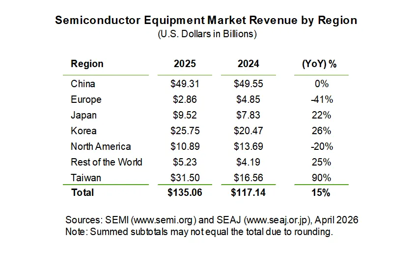
MILPITAS, Calif. – April 7, 2026 – Worldwide sales of semiconductor manufacturing equipment increased 15% to $135.1 billion in 2025 from $117.1 billion in 2024, driven by continued investment in advanced logic, memory, and AI-related capacity expansion, SEMI, the industry association representing the global electronics design and manufacturing supply chain, reported today. The data is available in the Worldwide Semiconductor Equipment Market Statistics (WWSEMS) report. 

SEMIIn 2025, the global front-end semiconductor equipment market posted solid growth, with wafer processing equipment sales increasing 12% and other front-end segments rising 13%. The expansion was driven primarily by continued investment in leading-edge logic and memory capacity, supported by AI-related demand and ongoing node and technology migrations.
The back-end equipment segment also recorded strong growth in 2025. Test equipment billings surged 55% year-over-year as AI devices and high-bandwidth memory (HBM) increased performance requirements and test intensity, while assembly and packaging equipment sales rose 21% as adoption of advanced packaging technologies continued to expand.

"Record semiconductor equipment billings of $135 billion in 2025 underscore the scale and urgency of the industry's buildout as AI accelerates demand for leading-edge logic, advanced memory and high-bandwidth architectures," said Ajit Manocha, SEMI President and CEO. "From wafer fab investments to the rapid rise of advanced packaging and test, the global ecosystem is expanding capacity and capability to support the next wave of innovation."

Regionally, semiconductor equipment spending remained concentrated in Asia in 2025, with China, Taiwan, and Korea together accounting for 79% of the global market, compared with 74% in 2024.

In 2025, spending in China remained near record levels at $49.3 billion, down just 0.5% from the prior year, as domestic chipmakers continued to invest in mature nodes and select advanced capacity. Equipment spending in Taiwan rose 90% year-over-year to a record $31.5 billion, reflecting AI- and HPC-driven capacity expansion. Korea increased 26% to $25.8 billion as investment in HBM and DRAM remained strong. 

In 2025, spending in China remained near record levels at $49.3 billion, down just 0.5% from the prior year, as domestic chipmakers continued to invest in mature nodes and select advanced capacity. Equipment spending in Taiwan rose 90% year-over-year to a record $31.5 billion, reflecting AI- and HPC-driven capacity expansion. Korea increased 26% to $25.8 billion as investment in HBM and DRAM remained strong. 

Japan recorded 22% growth to $9.5 billion, supported by continued investment in domestic advanced-node manufacturing. Europe declined 41% to $2.9 billion, marking a second consecutive year of contraction amid ongoing weakness in automotive and industrial demand. North America fell 20% to $10.9 billion as spending moderated following earlier capacity expansion. The rest of the world increased 25% to $5.2 billion, reflecting expanding activity in emerging semiconductor production markets.

Compiled from data submitted by members of SEMI and the Semiconductor Equipment Association of Japan (SEAJ), the WWSEMS report is a summary of the monthly billings figures for the global semiconductor equipment industry.

About SEMI Market Data

The Equipment Market Data Subscription (EMDS) from SEMI provides comprehensive market data for the global semiconductor equipment market. A subscription includes three reports: 

  • Monthly SEMI North American Billings Report, an early perspective of equipment market trends
  • Monthly Worldwide Semiconductor Equipment Market Statistics (WWSEMS), a detailed report of semiconductor equipment billings for seven regions and more than 22 market segments
  • Bi-annual Total Semiconductor Equipment Forecast – OEM Perspective, an outlook for the semiconductor equipment market

Download a sample EMDS report.

For more information or to subscribe, please contact SEMI Market Intelligence at [email protected]. Details on SEMI market data are available at SEMI Market Data.   

Follow SEMI Market Intelligence

Follow SEMI 

About SEMI

SEMI® is the global industry association connecting over 3,000 member companies and 1.5 million professionals worldwide across the semiconductor and electronics design and manufacturing supply chain. We accelerate member collaboration on solutions to top industry challenges through Advocacy, Workforce Development, Sustainability, Supply Chain Management and other programs. Our SEMICON® expositions and events, technology communities, standards and market intelligence help advance our members' business growth and innovations in design, devices, equipment, materials, services and software, enabling smarter, faster, more secure electronics. Visit www.semi.org, contact a regional office, and connect with SEMI on LinkedIn and X to learn more.


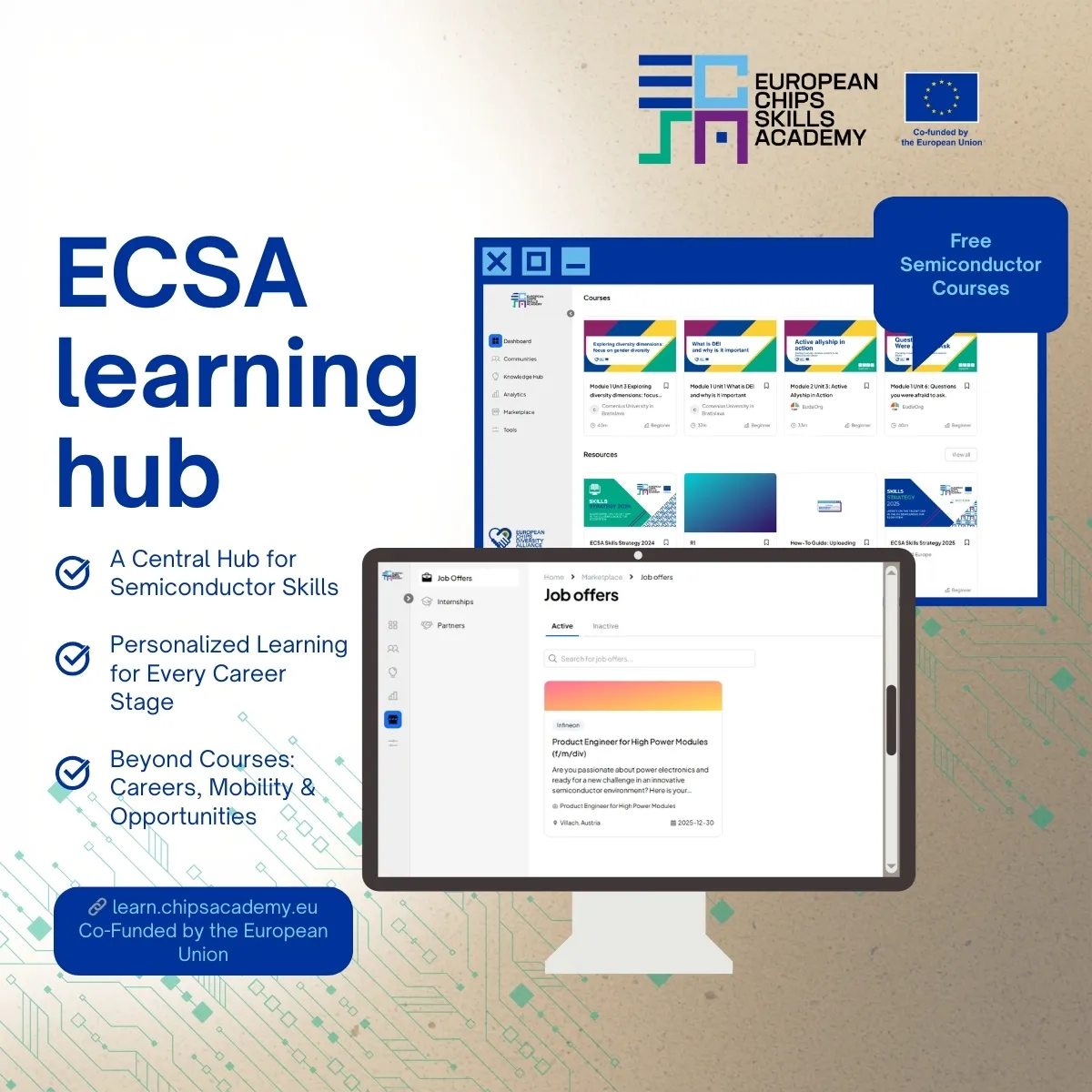
BRUSSELS — April 6, 2026 — The European Chips Skills Academy (ECSA), an European Union (EU)-funded initiative coordinated by SEMI Europe, today announced the official launch of its ECSA Learning Platform, a new digital hub with a full suite of training courses designed to support the development of semiconductor skills across Europe. With over 60 introductory to intermediate lessons, the platform brings together learning resources, collaboration spaces, and career opportunities to help students, researchers, and professionals build expertise in microelectronics and connect with the broader semiconductor ecosystem. 

Developed with input from industry and academic partners, the platform features a Knowledge Hub with curated learning materials and courses, community spaces for collaboration, and a marketplace for jobs and internships within the semiconductor value chain. Integrated learning analytics allow students to track their progress and support continuous professional development. All courses provided by ECSA partners are made entirely free for learners, supporting equal access to opportunity across Europe. 

“The launch of the ECSA Platform marks an important milestone in our mission to strengthen Europe’s semiconductor skills ecosystem and grow our workforce,” said Christopher Frieling, Director, Advocacy and Public Policy, SEMI Europe. “By bringing together education, industry insights, and career opportunities in one place, the platform helps connect talent with the skills and opportunities needed to support the future of Europe’s semiconductor industry.”

The platform is now open to students, educators, researchers, and professionals interested in exploring learning opportunities and careers within the semiconductor ecosystem. For companies and educators interested in listing employment opportunities or educational content on the ECSA Platform, please contact Victoria Cummings at [email protected]. 

Explore the platform: https://learn.chipsacademy.eu/

About SEMI

SEMI® is the global industry association connecting over 3,000 member companies and 1.5 million professionals worldwide across the semiconductor and electronics design and manufacturing supply chain. We accelerate member collaboration on solutions to top industry challenges through Advocacy, Workforce Development, Sustainability, Supply Chain Management, and other programs. Our SEMICON® expositions and events, technology communities, standards, and market intelligence help advance our members’ business growth and innovations in design, devices, equipment, materials, services, and software, enabling smarter, faster, more secure electronics. Visit www.semi.org, contact a regional office, and connect with SEMI on LinkedIn to learn more.

About ECSA

Launched in October 2023, the European Chips Skills Academy (ECSA) addresses skills shortages across Europe's semiconductor sector. The initiative collaborates closely with industry, academia, and policymakers to upskill, reskill, and attract new talent to the semiconductor workforce, supporting Europe's digital transition and sustainable growth. Visit https://chipsacademy.eu and connect with ECSA on LinkedIn and Instagram to learn more.

WASHINGTON, D.C. – April 2, 2026 – SEMI, the industry association serving the global semiconductor and electronics design and manufacturing supply chain, today announced Mary Bischoping as Senior Director of Public Policy and Advocacy. In her role, Bischoping will advance SEMI’s engagement with U.S. federal policymakers and stakeholders and lead strategy for policies related to supply chain resilience, intellectual property, U.S. tax policy, and emerging technologies, including AI and quantum.

A black text on a white background

Description automatically generated“Mary brings a rare combination of public policy expertise spanning technology, foreign policy, and government oversight—an invaluable addition as SEMI continues to advocate for forward-looking policies that reinforce the strength and resilience of the U.S. semiconductor industry,” said Royal Kastens, Vice President of Global Public Policy and Advocacy at SEMI. “We are excited to welcome her to the SEMI team and look forward to the impact she will have working alongside our members and policymakers.”

Based in Washington, D.C., Bischoping brings a decade of legal and public policy expertise to the role. Most recently, she was appointed as Deputy Assistant Secretary for the Bureau of Emerging Threats at the U.S. Department of State, where she led the department’s cybersecurity, AI, critical infrastructure, and outer space portfolios. She also served as Senior Counsel and Subcommittee Staff Director to the U.S. House Foreign Affairs Committee. 

Earlier in her career, Bischoping worked as a Judicial Law Clerk on the U.S. Court of Appeals for the Third Circuit and practiced as an attorney at Gibson Dunn & Crutcher LLP. She holds a J.D. from the University of Virginia School of Law and a B.A. from the University of California, Los Angeles.

View SEMI’s 2026 U.S. Policy Strategy to learn more about SEMI’s top policy priorities. For updates on SEMI’s public policy efforts and developments, visit SEMI Global Advocacy.

About SEMI

SEMI® is the global industry association connecting over 3,000 member companies and 1.5 million professionals worldwide across the semiconductor and electronics design and manufacturing supply chain. We accelerate member collaboration on solutions to top industry challenges through Advocacy, Workforce Development, Sustainability, Supply Chain Management and other programs. Our SEMICON® expositions and events, technology communities, standards and market intelligence help advance our members’ business growth and innovations in design, devices, equipment, materials, services and software, enabling smarter, faster, more secure electronics. Visit www.semi.org, contact a regional office, and connect with SEMI on LinkedIn and X to learn more.

BRUSSELS — April 14, 2026 — The SEMI Europe Policy Forum Brussels 2026 to be held on June 3 will bring together industry leaders, economists, policymakers, and technology experts to examine how geopolitical dynamics are transforming the global semiconductor landscape and to identify concrete pathways for reinforcing Europe’s leadership role.

As geopolitical forces rapidly and drastically reshape global markets, technological development, supply chains, and long-term strategic planning, these shifts present both profound challenges and unprecedented opportunities for regions prepared to act with vision and determination. SEMI Europe is committed to engaging with all stakeholders to advocate for a comprehensive Chips Act 2.0 initiative that will address existing gaps in the current framework. This next edition of the European Chips Act will help solidify Europe’s position in the global semiconductor sector, boost competitiveness, and enhance security.

“Supply chain resilience has become a strategic imperative,” said Ajit Manocha, President and CEO of SEMI. “From materials to manufacturing to logistics, we must strengthen coordination across every layer of the value chain to ensure readiness for future disruptions on a global scale.” 

The forum, themed Strengthening Europe’s Compass in the Perfect Storm, promotes collaboration between industry and policymakers across Europe to address complex transnational challenges facing the semiconductor ecosystem. As global competition intensifies, the event will focus on strengthening Europe’s supply chain resilience, aligning innovation with long-term geopolitical realities, and building strategic partnerships across borders.

“Geopolitics, technology, and industrial policy can no longer be addressed in isolation,” said Laith Altimime, President of SEMI Europe. “This forum creates a critical space for leaders across the value chain to work together, anticipate risks, and define Europe’s long-term strategic advantage in a rapidly shifting global environment.”

Through dialogue and shared insights, the forum advocates for a unified, competitive, and sustainable semiconductor ecosystem in Europe by strengthening technological leadership while addressing challenges that no single nation or company can solve alone. 

To attend the forum, please register your interest online or contact [email protected]​. Seating is limited. 

For more details, please visit the SEMI Europe Policy Forum Brussels 2026 website and connect with SEMI Europe on LinkedIn @SEMIEurope (#PolicyForumBrussels).  

About SEMI  

SEMI® is the global industry association connecting over 3,000 member companies and 1.5 million professionals worldwide across the semiconductor and electronics design and manufacturing supply chain. We accelerate member collaboration on solutions to top industry challenges through Advocacy, Workforce Development, Sustainability, Supply Chain Management and other programs. Our SEMICON® expositions and events, technology communities, standards and market intelligence help advance our members’ business growth and innovations in design, devices, equipment, materials, services and software, enabling smarter, faster, more secure electronics. Visit www.semi.org, contact a regional office, and connect with SEMI on LinkedIn and X to learn more.  

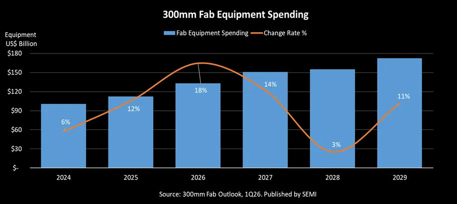
MILPITAS, Calif. – April 1, 2026 – Worldwide 300mm fab equipment spending is expected to increase 18% to $133 billion in 2026 and 14% to $151 billion in 2027, SEMI reported today in its latest 300mm Fab Outlook. This strong growth reflects surging AI chip demand for data centers and edge devices, as well as the growing commitment to semiconductor self-sufficiency across key regions through localized industrial ecosystems and supply chain restructuring.

Looking further out, the report projects investment will continue to increase 3% to $155 billion in 2028 and another 11% to $172 billion in 2029, respectively.

“AI is resetting the scale of semiconductor manufacturing investment,” said Ajit Manocha, President and CEO of SEMI. “With global 300mm fab equipment spending projected to exceed $150 billion in 2027 for the first time, the industry is making historic, sustained commitments to the advanced capacity and resilient supply chains needed to power the AI era.”


Segment Growth

The Logic & Micro segment is expected to spearhead equipment expansion with $228 billion in total investments from 2027 to 2029 mainly due to strong foundry sector demand, driven by sub-2nm cutting-edge capacity investments. Advanced node technology is essential to enhance chip performance and power efficiency to meet rigorous chip design requirements for various AI applications. More advanced node technology is expected to enter volume production from 2027 to 2029. Additionally, AI performance improvements are anticipated to drive massive growth in various edge AI devices. Beyond advanced nodes, demand across all nodes and various electronics devices is anticipated to grow moderately, supporting investment in mature nodes as well.

The memory segment is projected to rank second in equipment spending, totaling $175 billion from 2027 to 2029. This period marks the start of a new growth cycle for the segment. Within the memory category, DRAM equipment spending is expected to reach $111 billion cumulatively from 2027 to 2029, while 3D NAND equipment spending is estimated to be $62 billion during the same time frame. 

The demand for memory has significantly increased due to AI training and inference. AI training has notably driven up the demand for High Bandwidth Memory (HBM), while model inference has created substantial demand for storage capacity, thus boosting the growth of NAND Flash applications in data centers. This strong demand has led to sustained high levels of investment in the memory supply chain over the near and long term, helping to cushion potential downturns from traditional memory cycle fluctuations.

Regional Investment Trends

Global 300mm fab equipment investment is expected to remain broadly distributed across the major semiconductor manufacturing regions from 2027 to 2029, reflecting a mix of advanced-node expansion, memory capacity additions, and policy-supported supply chain localization. China, Taiwan, Korea, and the Americas are each expected to see substantial levels of spending during the period, while Japan, Europe & Middle East, and Southeast Asia also continue to expand investment from a smaller base. 

In China, investment is expected to remain supported by ongoing domestic capacity expansion and national initiatives aimed at strengthening semiconductor manufacturing capabilities. In the Taiwan region, spending is projected to be driven primarily by continued expansion of leading-edge foundry capacity, including 2nm and sub-2nm technologies. Korea’s investment outlook remains closely tied to the memory sector, where AI-related demand is supporting another cycle of capacity and technology upgrades. In the Americas, spending is expected to be underpinned by advanced process expansion and broader efforts to strengthen domestic manufacturing ecosystems. 

Japan, Europe & Middle East, and Southeast Asia are also expected to post meaningful growth through 2029. In these regions, equipment investment is supported by a combination of government incentives, supply chain resilience strategies, and targeted efforts to expand semiconductor manufacturing capacity.

Part of the SEMI Fab Forecast database, the SEMI 300mm Fab Outlook lists 404 facilities and lines globally. The report reflects 198 updates and 9 new fabs/lines projects since its last publication in December 2025. 

For more information on the report or to subscribe, please contact the SEMI Market Intelligence Team at [email protected]. Details on SEMI market data are available at SEMI Market Intelligence.  

Follow SEMI 

About SEMI

SEMI® is the global industry association connecting over 3,000 member companies and 1.5 million professionals worldwide across the semiconductor and electronics design and manufacturing supply chain. We accelerate member collaboration on solutions to top industry challenges through Advocacy, Workforce Development, Sustainability, Supply Chain Management and other programs. Our SEMICON® expositions and events, technology communities, standards and market intelligence help advance our members’ business growth and innovations in design, devices, equipment, materials, services and software, enabling smarter, faster, more secure electronics. Visit www.semi.org, contact a regional office, and connect with SEMI on LinkedIn and X to learn more

BRUSSELS – March 26, 2026 – SEMI Europe today participated in the European Commission’s Implementation Dialogue on the Chips Act, chaired by Henna Virkkunen, Executive Vice-President of the European Commission for Tech Sovereignty, Security and Democracy. As a key association representing the global electronics manufacturing and design supply chain in the region, SEMI Europe commends the European Commission for coordinating the Chips Act 2.0 Report, in consultation with leading semiconductor companies, to help define the future direction of Europe’s semiconductor policy and investment framework.

In this context, the Implementation Dialogue provided a valuable platform to assess progress under the European Chips Act and to gather concrete recommendations for its upcoming revision, commonly referred to as “Chips Act 2.0.” SEMI Europe strongly supports this consultative approach, which helps ensure that policy objectives are achieved while minimizing administrative and compliance burden for industry.

“SEMI Europe applauds the European Commission for fostering an open and constructive dialogue with industry at a critical moment for Europe’s semiconductor ecosystem,” said Laith Altimime, President of SEMI Europe. “This is a defining moment. With focused execution and unified commitment across institutions and industry, Europe can secure its position as a global leader in semiconductor innovation and manufacturing for decades to come.”

During the dialogue, SEMI Europe highlighted its significant contribution to the policy discussion through its SEMI Europe Chips Act Report published last year, which outlined 30 recommendations aimed at strengthening Europe’s semiconductor ecosystem across the entire supply chain. These included regulatory simplification, accelerated permitting processes, targeted investment support, and measures to strengthen the resilience of the semiconductor supply chain.

SEMI, with its global footprint of over 3,000 members worldwide from across the entire semiconductor value chain, will remain a trusted partner to facilitate global collaboration and support the success of the European Chips Act and its potential “2.0.”

SEMI Europe Advocacy

Discover how SEMI Europe Advocacy & Public Policy supports the microelectronics industry across sustainability, trade, talent, and R&D—or become involved by contacting [email protected]. 

About SEMI

SEMI® is the global industry association connecting over 3,000 member companies and 1.5 million professionals worldwide across the semiconductor and electronics design and manufacturing supply chain. We accelerate member collaboration on solutions to top industry challenges through Advocacy, Workforce Development, Sustainability, Supply Chain Management, and other programs. Our SEMICON® expositions and events, technology communities, standards, and market intelligence help advance our members’ business growth and innovations in design, devices, equipment, materials, services, and software, enabling smarter, faster, more secure electronics. Visit www.semi.org, contact a regional office, and connect with SEMI on LinkedIn and X to learn more.