
downloadGroupGroupnoun_press release_995423_000000 copyGroupnoun_Feed_96767_000000Group 19noun_pictures_1817522_000000Member company iconResource item iconStore item iconGroup 19Group 19noun_Photo_2085192_000000 Copynoun_presentation_2096081_000000Group 19Group Copy 7noun_webinar_692730_000000Path
Skip to main content
Default Banner Image

SEMI Press Release

ID
semi-press-release

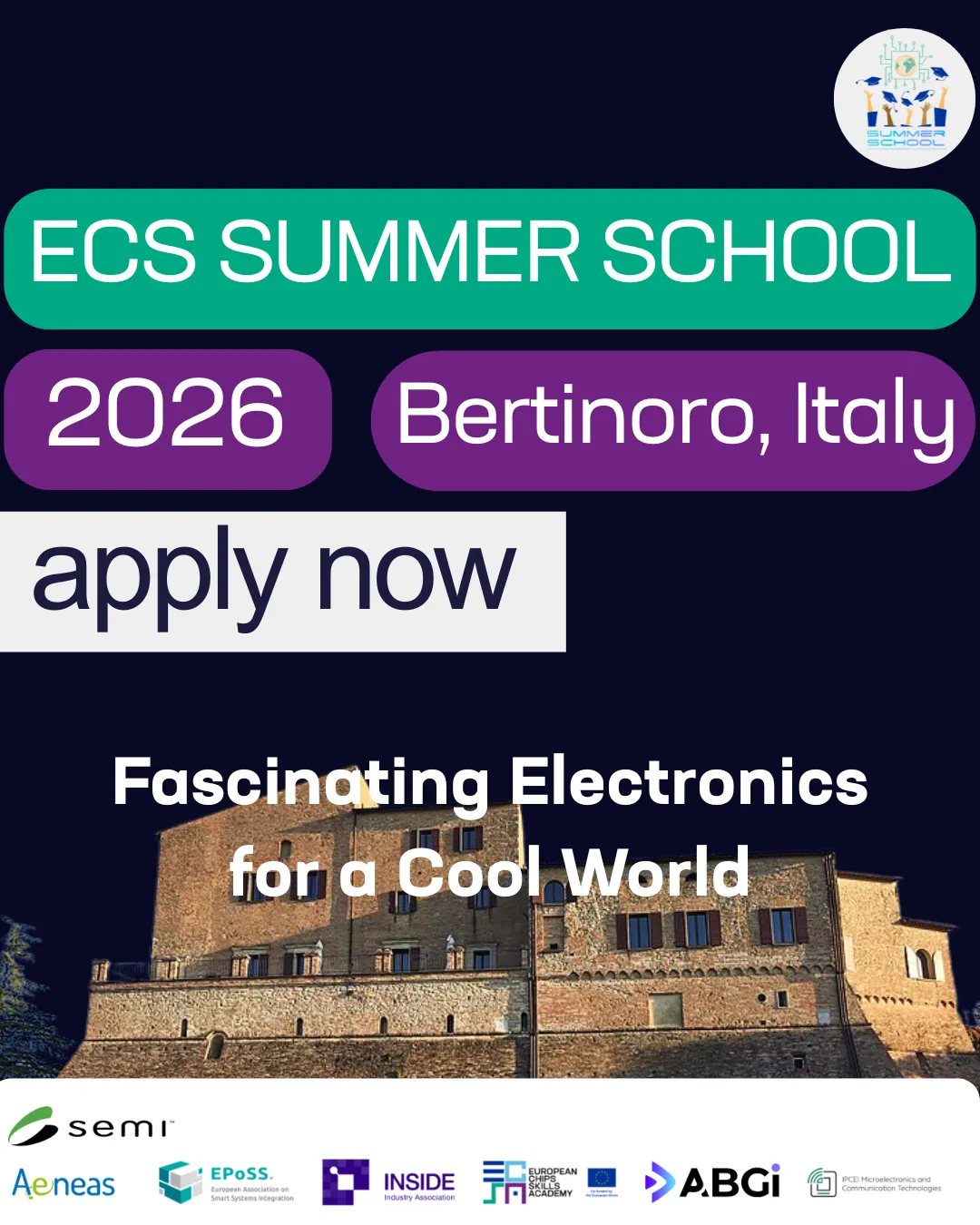
Brussels, Belgium —February 12, 2026 —The European Chips Skills Academy (ECSA), a European Union (EU)-funded project coordinated by SEMI Europe, in collaboration with industry partners AENEAS, EPoSS, and INSIDE, today announced that applications are open for the ECS Summer School. Taking place from 23 – 28 August 2026 at the University Residential Centre, University of Bologna, Bertinoro, Italy, the programme invites applications from undergraduate STEM students across the EU and associated countries. 
“Programmes such as the ECS Summer School are vital to motivating and developing the next generation of talent that will sustain Europe’s semiconductor workforce,” said Laith Altimime, President of SEMI Europe.

As Europe accelerates its transition to a digitally enabled future, demand for skilled professionals in microelectronics and semiconductor technologies continues to grow. The ECS Summer School offers a comprehensive, immersive learning experience designed to equip the next generation of engineers, researchers, and innovators with foundational and advanced insights into chip design, semiconductor fabrication, and embedded intelligent systems. 

“The ECS Summer School provides students with a strong entry point to acquire practical skills and form valuable connections with industry and academia,” said Patrick Cogez, Technical Director at AENEAS and ECSA lead partner for the organisation of the Summer School.

Programme Highlights
The curriculum spans four core domains of microelectronics:

  • Semiconductor Technology
  • Integrated Circuit Design
  • Digital Systems and Embedded Intelligence
  • Integration of Electronic Systems

This year’s summer school will be co-organized by ABGi and IPCEI ME/CT. Lectures, demonstrations, and interactive activities will be delivered by experts from leading universities, research institutes, and industry partners, complemented by career testimonies from engineers working in the field. 

Eligibility & Application Details
The Summer School is open to undergraduate students who will have completed at least two years of university study by the time of the event and who will still have at least one year remaining in their degree programme. Participants must be enrolled in a STEM (Science, Technology, Engineering, Mathematics) discipline at a university based in the EU or eligible associated country and possess a good command of English, as all activities will be conducted in English. 

Registration details, application requirements, and the full programme overview are available on the official ECS Summer School 2026 page. There are limited spots available, so the organisers encourage students to apply today.

About SEMI

SEMI® is the global industry association connecting over 3,000 member companies and 1.5 million professionals worldwide across the semiconductor and electronics design and manufacturing supply chain. We accelerate member collaboration on solutions to top industry challenges through Advocacy, Workforce Development, Sustainability, Supply Chain Management, and other programs. Our SEMICON® expositions and events, technology communities, standards, and market intelligence help advance our members’ business growth and innovations in design, devices, equipment, materials, services, and software, enabling smarter, faster, more secure electronics. Visit www.semi.org, contact a regional office, and connect with SEMI on LinkedIn and X to learn more.

About ECSA

Launched in October 2023, the European Chips Skills Academy (ECSA) addresses skills shortages across Europe's semiconductor sector. The initiative collaborates closely with industry, academia, and policymakers to upskill, reskill, and attract new talent to the semiconductor workforce, supporting Europe's digital transition and sustainable growth. Visit https://chipsacademy.eu and connect with ECSA on LinkedIn and Instagram to learn more.

About AENEAS

AENEAS, a not-for-profit industry association, aims to enhance the competitiveness of European industries in Electronic Components and Systems (ECS). It allows to influence RD&I policies, facilitates access to funding and offers networking opportunities. With over 550 members, it represents the full ECS value chain. Governed by a 20-member board from major companies, SMEs, and research centres, AENEAS advocates for the sector at the top European level. As a partner of the Chips Joint Undertaking, AENEAS represents the interest of its members in this tri-partite partnership between Industry, the European Commission and the participating states. AENEAS contributes to shaping and co-defining the Electronic Components and Systems Strategic Research and Innovation Agenda (ECS-SRIA). AENEAS stimulates and supports collaborative innovation to meet societal and economic challenges in a sustainable way. AENEAS is also operating the EUREKA funded programmes Xecs, PENTA and Euripides. More information: https://aeneas-office.org
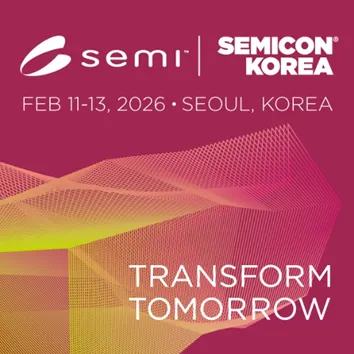
SEOUL, South Korea ─ February 10, 2026 ─ Fueled by the rapid advancement of AI and the widespread adoption of advanced applications, the semiconductor industry has moved beyond a traditional upcycle and entered a new phase of powerful momentum. Amid this shift, Korea’s semiconductor ecosystem—led by Samsung Electronics and SK hynix and supported by a broad range of materials, parts, and equipment companies—is reaching a critical inflection point. At this pivotal moment, SEMICON Korea 2026 will bring together the global semiconductor ecosystem to explore new business opportunities and present the future direction of technological innovation. The event will be held this week in Seoul from February 11-13. Registration is open.

Approximately 550 companies will showcase advanced semiconductor manufacturing technologies and solutions across more than 2,400 booths at SEMICON Korea 2026. Global chipmakers and design leaders—including NVIDIA, Samsung Electronics, SK hynix, Intel, Kioxia, Micron, and Sony—will join major equipment and materials companies such as ASML, Applied Materials, Lam Research, Tokyo Electron, and KLA, bringing together leaders from across the entire semiconductor value chain.

“As AI transforms every facet of semiconductor design and manufacturing, alignment across the global supply chain has never been more critical,” said SEMI Korea President Hyun Cha. “Korea’s vibrant semiconductor ecosystem holds a crucial position in shaping this new era. By strengthening collaboration and sharing a unified vision here at SEMICON Korea, we can accelerate innovation and ensure the industry is ready to meet the opportunities ahead.”

Under the theme “Transform Tomorrow,” this year’s event will present a platform for cutting-edge technologies and collaboration that will reshape the future amid a new industrial paradigm driven by AI. Over three days, more than 200 semiconductor experts will speak across over 30 conferences, covering key industry topics including advanced manufacturing technology, AI, smart manufacturing, metrology and inspection, test, compound power semiconductors, cybersecurity, market trends, investment opportunities, and global R&D collaboration.

This year’s event will take place at the largest scale in its history, spanning all halls (A, B, C, D, and E) of COEX, as well as the Grand Ballroom, Platz, The Westin Seoul Parnas, and the Grand InterContinental Seoul Parnas. As the rapid growth of Korea’s semiconductor industry has driven demand beyond the exhibition venue’s capacity, the event’s expansion into nearby hotels reflects the remarkable expansion of the industry itself.

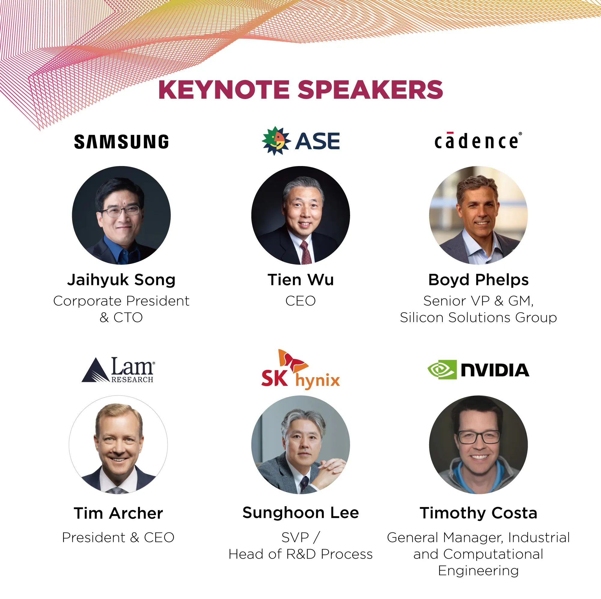
SEMICON Korea 2026 will open with a keynote session featuring Samsung Electronics, ASE, Cadence, Lam Research, SK hynix, and NVIDIA.

SEMICON Korea 2026 Keynotes

  • Beyond ZFLOPS: What's Next? - Architecting the Future of AI Systems
    • Jaihyuk Song, Corporate President and CTO, Samsung Electronics
  • Advanced Packaging and the Future of System Optimization
    • Tien Wu, CEO, ASE
  • Building Scalable Infrastructure for the AI Factories of Tomorrow: Cadence’s End-to-end Approach
    • Boyd Phelps, Senior Vice President and General Manager, Silicon Solutions Group, Cadence Design Systems
  • The Velocity Imperative
    • Tim Archer, President and CEO, Lam Research
  • The Inflection Point Has Arrived: Driving Innovation Towards Future of Memory Technology
    • Sunghoon Lee, Senior Vice President and Head of R&D Process, SK hynix
  • AI Supercomputing for Next-Generation Semiconductor Design and Manufacturing
    • Timothy Costa, General Manager, Industrial and Computational Engineering, NVIDIA

Key Highlights of SEMICON Korea 2026

Technology Conferences

  • SEMI Technology Symposium (STS): Industry experts will share advanced technology trends in six sessions on semiconductor manufacturing:
    • Advanced Lithography
    • Advanced Materials & Process Technology
    • Device Technology
    • Plasma Science & Etching Technology
    • CMP & Cleaning Technology
    • Advanced Packaging
  • AI Summit: Co-hosted by SEMI and KAIST, the AI Summit will bring together KAIST faculty along with representatives from Samsung Electronics, SK hynix, and global equipment leaders to present technology strategies and future roadmaps driving AI-powered industrial innovation, while sharing key solutions that will accelerate the AI era.
  • Test Forum: Industry experts will explore how next-generation AI-driven test strategies, advanced automated test equipment (ATE), and sophisticated data analytics are supporting the development of next-generation semiconductor devices.
  • Compound Power Semiconductor Summit: This summit will examine the entire compound power semiconductor value chain—from manufacturing (single crystal, epi-wafer, ion implantation) to high-performance power system integration (devices and modules)—while presenting the technology and market outlook for wide bandgap (WBG) semiconductors.
  • Cybersecurity Forum: Global experts will address critical cybersecurity challenges across the semiconductor ecosystem, including compliance, fab security, and AI data governance, while sharing collaborative strategies to strengthen digital trust.
  • MI (Metrology & Inspection) Forum: As advanced semiconductor manufacturing grows increasingly complex, experts from device and equipment companies will present the latest trends and solutions in metrology and inspection technologies.
  • Smart Manufacturing Forum: This forum will highlight how AI, digital twins, and real-time data technologies are transforming semiconductor manufacturing, sharing the latest trends and success cases for the era of autonomous manufacturing.
  • Global Semiconductor Regulatory Outlook Forum: The forum will examine international and domestic regulatory trends, evolving energy policies, and customer-centric compliance strategies shaping the semiconductor industry.

Business Forums

  • Market Trends Forum: In collaboration with global research organizations, SEMI will provide a comprehensive analysis of macroeconomic conditions, regulatory changes, and key trends across the semiconductor market, packaging, equipment, and materials sectors—supporting strategic decision-making in a rapidly evolving industry.
  • U.S. Investment Forum: Co-hosted by SEMI Korea and SelectUSA, this session will introduce the U.S. investment environment and market outlook to Korean companies while providing opportunities for direct engagement with major semiconductor clusters and regional Economic Development Organizations (EDOs).
  • Startup Summit: Semiconductor and display startups will showcase innovative technologies and explore growth opportunities through networking with industry leaders and investors.
  • Netherlands-Korea Semiconductor Tech Seminar: Companies and research institutes from the Netherlands and Korea will gather to strengthen semiconductor R&D collaboration through technology exchange, joint research, and strategic partnerships.
  • Supplier Search Program: This program offers targeted networking opportunities to support domestic semiconductor materials, components, and equipment companies expanding into global markets. Industry leaders such as Intel, Kioxia, Lam Research, Micron, and Sony will participate in approximately 100 business meetings with Korean companies.

Workforce Development Initiatives

To address the growing need for talent in the semiconductor industry, SEMICON Korea 2026 will once again host dedicated workforce development programs.

  • Meet the Experts!: A mentoring program designed to nurture future semiconductor talent will connect STEM university students with engineers from leading semiconductor companies, who will provide practical guidance on career development, job roles, and industry insights.
  • Technology Tutorials: Foundational training sessions will be offered for STEM students and junior engineers, covering the fundamentals of six key semiconductor manufacturing processes: lithography, deposition, device, plasma and etching, CMP and cleaning, and packaging.

Full details are available on the SEMICON Korea 2026 website.

About SEMI

SEMI® is the global industry association connecting over 3,000 member companies and 1.5 million professionals worldwide across the semiconductor and electronics design and manufacturing supply chain. We accelerate member collaboration on solutions to top industry challenges through Advocacy, Workforce Development, Sustainability, Supply Chain Management and other programs. Our SEMICON® expositions and events, technology communities, standards and market intelligence help advance our members’ business growth and innovations in design, devices, equipment, materials, services and software, enabling smarter, faster, more secure electronics. Visit www.semi.org, contact a regional office, and connect with SEMI on LinkedIn and X to learn more.

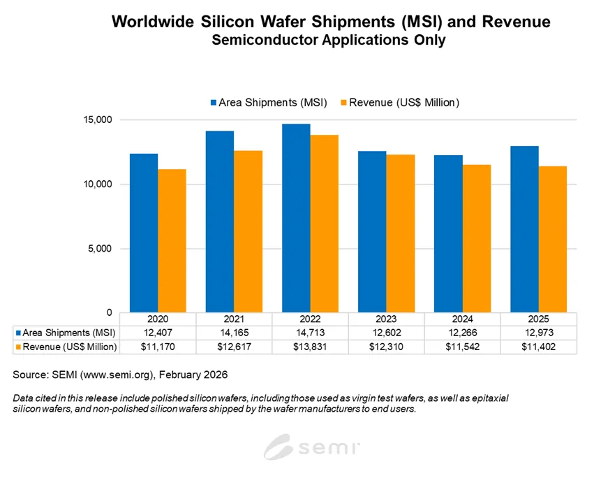
MILPITAS, Calif. — February 10, 2026 — Worldwide silicon wafer shipments in 2025 increased 5.8% to 12,973 million square inches (MSI) while wafer revenue slipped 1.2% to $11.4 billion over the same period, the SEMI Silicon Manufacturers Group (SMG) reported in its year-end analysis of the silicon wafer industry. 

SEMI Logo2025 marks an inflection year for wafer shipments, with silicon MSI resuming growth supported by strong demand for advanced epitaxial wafers in logic and polished wafers for high-bandwidth memory (HBM), driven by AI applications. Softness in wafer revenue is mostly attributed to the slow momentum in traditional semiconductor applications where the demand and pricing environment are yet to improve.

“The 2025–2026 wafer market is shaped by diverging trends across technology nodes,” said Ginji Yada, Chairman of SEMI SMG and Executive Office Deputy General Manager, Sales and Marketing Division at SUMCO Corporation. “Demand for 300mm wafers remains strong in advanced applications, particularly in AI-driven logic and high-bandwidth memory (HBM), supported by the ongoing adoption of sub-3nm processes. These technology transitions are driving increased requirements for wafer quality and consistency, reinforcing the need for advanced material solutions. Investments in data centers and generative AI continue to underpin demand in leading-edge segments, where performance and reliability are critical. 

“In contrast, the legacy semiconductor segment shows gradual signs of stabilization. Wafer and chip inventory levels in mature-node applications—such as automotive, industrial, and consumer electronics—have begun to normalize after extended inventory adjustments. While supply-demand conditions are improving sequentially, the pace of recovery remains moderate, with demand recovery still sensitive to macroeconomic factors and end-market dynamics. As a result, the overall market outlook reflects a two-track trajectory: sustained demand and technical advancement in advanced nodes, alongside a cautious and incremental rebound for demand in mature technology segments.”

MSI

Silicon wafers are the fundamental building material for the majority of semiconductors, which are vital components of all electronic devices. The highly engineered thin disks are produced in diameters of up to 300 mm and serve as the substrate material on which most semiconductors are fabricated.

The SMG is a sub-committee of the SEMI Electronic Materials Group (EMG) and is open to SEMI members involved in manufacturing polycrystalline silicon, monocrystalline silicon or silicon wafers (e.g., as cut, polished, epitaxial). The SMG facilitates collective efforts on issues related to the silicon industry, including the development of statistics about the silicon industry.

For more information, visit SEMI Worldwide Silicon Wafer Shipment Statistics or contact the SEMI Market Intelligence Team at [email protected]. Additional details on SEMI market data are available at SEMI Market Intelligence.

Follow SEMI

About SEMI

SEMI® is the global industry association connecting over 3,000 member companies and 1.5 million professionals worldwide across the semiconductor and electronics design and manufacturing supply chain. We accelerate member collaboration on solutions to top industry challenges through Advocacy, Workforce Development, Sustainability, Supply Chain Management and other programs. Our SEMICON® expositions and events, technology communities, standards and market intelligence help advance our members’ business growth and innovations in design, devices, equipment, materials, services and software, enabling smarter, faster, more secure electronics. Visit www.semi.org, contact a regional office, and connect with SEMI on LinkedIn and X to learn more.


SOPOT, Poland — January 30, 2026 — Leading industry experts, economists, policymakers, and technology leaders will gather at the SEMI Industry Strategy Symposium Europe (ISS Europe) 2026, March 11–13 in Sopot, Poland, to examine how geopolitical dynamics are reshaping the global semiconductor landscape. This year’s symposium will focus on how Europe can navigate increasing geopolitical complexity, strengthen supply chain resilience, and reinforce its global competitiveness in an increasingly fragmented landscape. Registration is open.

Themed Navigating Geopolitics: Shaping Europe’s Future, ISS Europe 2026 will explore the intersection of technological innovation and geopolitical transformation. Experts will examine how Europe can strengthen its position within the global semiconductor supply chain, forge new partnerships, and develop a unified, competitive, and sustainable strategy to thrive in a rapidly evolving world.

“These are defining times for Europe’s semiconductor industry as we navigate an increasingly complex geopolitical landscape,” said Laith Altimime, President of SEMI Europe. “To secure our technological leadership and long-term competitiveness, we must build stronger cross-border collaboration, accelerate innovation, and shape a unified European strategy. ISS Europe 2026 provides a critical platform for aligning industry, academia, and policy to ensure Europe’s leadership in a rapidly shifting global economy.”

ISS Europe 2026 Highlights

ISS Executive Opening
Executives will examine the current semiconductor landscape and outline strategic priorities to reinforce Europe’s global competitiveness.

Session 1: Geopolitical Dynamics Impacting Market Success
Thought leaders will explore how shifting global power structures are reshaping semiconductor supply chains and assess Europe’s opportunities to strengthen competitiveness and technological leadership.

Session 2: Securing Europe’s Sovereignty: Collaboration for Resilient Supply Chains
Speakers will delve into how innovation, manufacturing excellence, and stronger supply partnerships can build resilience, reduce risk, and support long-term sustainability across the value chain.

Session 3: From Lab to Fab: Translating Innovation into Sustainable Manufacturing
Industry experts will examine the enablers of European competitiveness—from research and innovation capacity to talent development and industrial coordination.

Session 4: Strategic R&D & Disruptive Manufacturing
Participants will discover how advanced R&D and disruptive manufacturing approaches can accelerate performance, efficiency, and industrial strength in next-generation semiconductor technologies.

Session 5: Startup Innovations Driving the Next Era of Industry
Experts will spotlight how agile, tech-driven startups are reshaping value chains and enabling Europe’s competitive edge across materials, design, manufacturing, and automation.

Business Networking

ISS Europe 2026 will feature several networking activities, including a welcome reception and an exclusive gala dinner, where attendees can connect with peers to explore new business and collaboration opportunities. 

Sponsors

For more details, please visit the Industry Strategy Symposium Europe (ISS Europe) 2026 website and connect with SEMI Europe on LinkedIn @SEMIEurope (#ISSEurope).

About SEMI 

SEMI® is the global industry association connecting over 3,000 member companies and 1.5 million professionals worldwide across the semiconductor and electronics design and manufacturing supply chain. We accelerate member collaboration on solutions to top industry challenges through Advocacy, Workforce Development, Sustainability, Supply Chain Management and other programs. Our SEMICON® expositions and events, technology communities, standards and market intelligence help advance our members’ business growth and innovations in design, devices, equipment, materials, services and software, enabling smarter, faster, more secure electronics. Visit www.semi.org, contact a regional office, and connect with SEMI on LinkedIn  and  X  to learn more.  

MILPITAS, Calif. — January 28, 2026 — SEMI, the industry association serving the global semiconductor and electronics design and manufacturing supply chain, today announced its 2026 U.S. Policy Strategy: Securing the Semiconductor Supply Chain to Enable American AI Leadership designed to strengthen U.S. competitiveness, sustain long-term market investment, and support innovation across the full semiconductor ecosystem. These focal points reflect SEMI’s role as a trusted partner to policymakers and its commitment to advancing practical, coordinated, and industry-informed solutions that reinforce U.S. competitiveness in a highly integrated global industry.

semi logo“The semiconductor industry is vital to every facet of the modern economy, from artificial intelligence and advanced manufacturing to national security and workforce development,” said Ajit Manocha, president and CEO of SEMI. “As global competition intensifies and policy frameworks continue to evolve, the ability of the U.S. to maintain leadership in semiconductor design, manufacturing, and innovation will depend on clear, predictable, and forward-looking policy execution.”


SEMI policy priorities this year focus on providing certainty, enabling long-term investment, and ensuring the U.S. remains connected to the global network that makes semiconductor manufacturing resilient and sustainable. The SEMI 2026 U.S. Policy Strategy emphasizes five interconnected areas critical to strengthening U.S. leadership:

  • Balanced trade policy that preserves access to critical inputs, avoids overlapping tariffs on the same product, and supports market access for U.S. companies while advancing national security objectives.
  • A national semiconductor workforce pipeline aligned with federal, state, and industry programs to address critical talent needs across the semiconductor ecosystem.
  • Long-term tax and R&D incentives that provide predictability for multi-year investments and support innovation across the full semiconductor supply chain, including upstream suppliers.
  • Continued implementation of the CHIPS and Science Act and pursuit of a forward-looking roadmap to sustain momentum and ensure authorized funding translates into capacity and innovation.
  • Pragmatic policies that balance environmental goals with the technological requirements of semiconductor manufacturing necessary for continued innovation.

These priorities underscore the importance of early and meaningful engagement with industry for policymakers. Given the complexity of semiconductor supply chains and the scale of investments involved, policies developed with technical input from industry are more likely to achieve their intended outcomes while avoiding unintended consequences.

SEMI’s 2026 U.S. Policy Strategy also highlights the importance of coordination with U.S. allies and partners, as well as continued support for public-private research partnerships. Semiconductor manufacturing relies on a global network of specialized materials, equipment, and expertise, and policies that are aligned internationally help strengthen supply chain resilience, protect shared security interests, and preserve U.S. competitiveness.

“SEMI’s approach is grounded in partnership,” said Joe Stockunas, president of SEMI Americas. “Our members are investing in the United States at historic levels, bringing thousands of good-paying, skilled jobs to communities across the country. Clear rules, predictable incentives, and coordinated policy execution give those investments the best chance to succeed. We look forward to continued collaboration with policymakers to ensure the U.S. semiconductor ecosystem remains strong, resilient, and globally competitive.”

The SEMI 2026 U.S. Policy Strategy positions the industry as a constructive partner in advancing policies that support economic growth, innovation, and national security. Through collaboration, credibility, and consistent engagement, SEMI is working to ensure that the next phase of U.S. semiconductor expansion delivers lasting benefits for the broader economy.

Visit SEMI Global Advocacy to learn more about public policy efforts and developments.

Follow SEMI

About SEMI
SEMI® is the global industry association connecting over 3,000 member companies and 1.5 million professionals worldwide across the semiconductor and electronics design and manufacturing supply chain. We accelerate member collaboration on solutions to top industry challenges through Advocacy, Workforce Development, Sustainability, Supply Chain Management and other programs. Our SEMICON® expositions and events, technology communities, standards and market intelligence help advance our members’ business growth and innovations in design, devices, equipment, materials, services and software, enabling smarter, faster, more secure electronics. Visit www.semi.org, contact a regional office, and connect with SEMI on LinkedIn and X to learn more.

MILPITAS, Calif. — January 22, 2026 — The FLEX Technology Summit will be held on February 24-26, 2026, at the Wigwam Arizona Resort in Phoenix, Arizona, celebrating 25 years of innovation in flexible hybrid electronics (FHE), printed electronics, and advanced packaging. This year’s theme, “Edge of Reality: Augmenting Flexible Hybrid Electronics with AI, Digital Twins, and XR,” will focus on how emerging technologies are transforming FHE and related fields. Registration is open.  

FLEX 2026 will feature keynotes, technical sessions, gap analyses, professional courses, industry tours, and a dynamic exhibit of solution providers showcasing the latest advancements in FHE, heterogeneous integration, MedTech, and more. Attendees will gain insights into cutting-edge equipment, processes, materials, and applications driving next-generation electronics. The event will also highlight innovations from public-private partnerships fostered by SEMI Technology Communities, FlexTech and Nano-Bio Materials Consortium (NMBC). 

“For 25 years, FLEX has been integral in uniting the industry, academia, and government—pushing the boundaries of what’s possible in flexible hybrid electronics,” said Gity Samadi, Senior Director of R&D Programs at SEMI. “This milestone is not just a celebration of our progress, but a look into what’s next. At FLEX Technology Summit, we’ll reflect on the innovations that built the foundation to today's technologies and explore the breakthroughs that will revolutionize the next 25 years.”

FLEX Technology Summit 2026 Keynote Presentations:

  • Michael D. McCreary, PhD, Chief Innovation Officer, Senior VP, E Ink
    Flexible ePaper Displays: From University Research to Global Corporation
  • Roozbeh Ghaffari, Co-Founder, Chief Executive Office, Epicore Biosystems, Inc.
    Wearable Microfluidic Systems for Personalized Hydration and Health Management
  • Lindsay Pack Moll, Chief Executive Officer, InnovaFlex USA 
    From Idea to Fab
  • Ani Kelkar, PhD, Partner, McKinsey & Company, Inc.
    Will Embodied AI Create Robotic Coworkers?
  • John A. Rogers, Director, Northwestern University
    Flexible Bioelectronics – From Exploratory Research to Medical Translation

Join FLEX 2026 to celebrate 25 years of innovation and explore the future of electronics at the intersection of flexibility, intelligence, and connectivity. Register today at https://semi.swoogo.com/FLEX_2026. 

About SEMI

SEMI® is the global industry association connecting over 3,000 member companies and 1.5 million professionals worldwide across the semiconductor and electronics design and manufacturing supply chain. We accelerate member collaboration on solutions to top industry challenges through Advocacy, Workforce Development, Sustainability, Supply Chain Management and other programs. Our SEMICON® expositions and events, technology communities, standards and market intelligence help advance our members’ business growth and innovations in design, devices, equipment, materials, services and software, enabling smarter, faster, more secure electronics. Visit www.semi.org, contact a regional office, and connect with SEMI on LinkedIn and X to learn more.  

MILPITAS, Calif. — January 15, 2026 — SEMI, the leading industry association representing the global semiconductor and electronics design and manufacturing supply chain, today released a statement in response to President Trump signing two Presidential Proclamations addressing U.S. semiconductor and critical mineral supply chains. The first imposes a 25 percent tariff on certain advanced computing chips while exempting those imports for specific use cases. It also directs executive branch officials to continue negotiating with trading partners and signals that broader tariffs, along with a tariff offset program to encourage domestic manufacturing, may be implemented in the near future. 

A picture containing text, clipart

Description automatically generated

The second Proclamation focuses on critical minerals, directing officials to engage with trading partners to reduce vulnerabilities in these supply chains and authorizing the United States to take further action if negotiations fail to mitigate the risks. These actions follow the conclusion of investigations initiated by the U.S. Department of Commerce in April 2025 to assess the national security implications of imports of semiconductors, semiconductor manufacturing equipment, and their derivatives, as well as processed critical minerals and their derivatives.

SEMI released the following statement in response to the actions announced by the White House:

“SEMI supports the Administration’s commitment to strengthening the U.S. semiconductor and critical mineral supply chains and shares its position that semiconductors, semiconductor manufacturing equipment, and critical minerals are vital for U.S. economic and national security.  

“Following yesterday's announcement, we are encouraged to see the Administration implement a targeted approach for both actions and establish a non-stacking framework consistent with SEMI’s advocacy. This demonstrates responsiveness to industry concerns about minimizing supply chain disruptions while addressing specific national security priorities.

“As reflected in SEMI’s public comments, the semiconductor industry is making historic investments to expand domestic manufacturing capacity. At the same time, the global semiconductor supply chain consists of highly specialized and interdependent segments that cannot be easily replicated or relocated within a commercially viable timeframe. SEMI appreciates the Administration’s measured approach and efforts to avoid unintentionally constraining ongoing U.S. manufacturing expansions and global competitiveness.

“SEMI urges the Administration to continue engaging closely with industry to ensure any further trade actions account for commercial and operational realities, and minimize unintended impacts on global supply chains. SEMI looks forward to working with the Administration on the implementation of these trade actions and will continue to advocate for approaches that advance the Administration’s objectives of strengthening the resilience of the U.S. semiconductor supply chain and enhancing U.S. global competitiveness.”

Visit SEMI Global Advocacy to learn more about public policy efforts and developments.

About SEMI

SEMI® is the global industry association connecting over 3,000 member companies and 1.5 million professionals worldwide across the semiconductor and electronics design and manufacturing supply chain. We accelerate member collaboration on solutions to top industry challenges through Advocacy, Workforce Development, Sustainability, Supply Chain Management, and other programs. Our SEMICON® expositions and events, technology communities, standards, and market intelligence help advance our members’ business growth and innovations in design, devices, equipment, materials, services, and software, which enable smarter, faster, and more secure electronics. Visit www.semi.org, contact a regional office, and connect with SEMI on LinkedIn and X to learn more.

MILPITAS, Calif. — January 20, 2026 — The SEMI Foundation today announced it has been officially approved by the U.S. Department of Labor (USDOL) as a National Apprenticeship Sponsor. This is a major milestone that strengthens industry led workforce development and expands access to high quality earn and learn pathways across the U.S. semiconductor ecosystem.

This designation aligns with the Administration’s broader America’s talent and workforce strategy, which emphasizes registered apprenticeships as a critical tool for building a resilient, competitive, and skilled workforce in strategic industries. As a national sponsor, the SEMI Foundation will work directly with employers to design, register, and scale apprenticeship programs that meet evolving industry needs while providing workers with clear, high value career pathways.

“Apprenticeships are a proven way to connect talent to opportunity while meeting real employer demand,” said Michelle Williams, Executive Director of the SEMI Foundation. “Becoming a national apprenticeship sponsor allows us to move faster, scale smarter, and support companies across the semiconductor supply chain as they build the workforce they need to compete globally.”

A Strategic Advantage for SEMI Member Companies

The SEMI Foundation is the nonprofit arm of SEMI, the industry association serving the global semiconductor and electronics design and manufacturing supply chain. As part of the Foundation’s new role, SEMI member companies will receive priority access to apprenticeship sponsorship, technical assistance, and program development support. Over time, the Foundation will expand access to additional employers across the ecosystem, ensuring alignment, quality, and consistency at scale.

Through the national sponsorship model, the SEMI Foundation will:

  • Reduce administrative and regulatory barriers for employers launching apprenticeships

  • Support standardized, industry aligned apprenticeship frameworks

  • Enable faster deployment across multiple states and regions

  • Ensure programs meet federal quality standards while remaining employer driven

Connecting Apprenticeship to a National Workforce Strategy

The SEMI Foundation’s apprenticeship sponsorship will be closely coordinated with the National Network for Microelectronics Education NNME, a national initiative funded by the U.S. National Science Foundation (NSF) and operated by the Foundation to strengthen semiconductor education and workforce development through regional collaboration.

Through NNME Regional Nodes, apprenticeship programs will be aligned with local and regional employer demand, education and training providers, workforce boards, and economic development organizations. This integrated approach ensures apprenticeships are not standalone programs, but part of a connected, scalable national talent system that supports students, workers, and employers at every stage.

“Registered apprenticeships are a cornerstone of a modern workforce system,” said Mike Glavin, Director of Workforce Development at the SEMI Foundation. “By embedding apprenticeships into our national and regional strategies, we’re creating pathways that are both locally responsive and nationally aligned.”

What’s Next

The SEMI Foundation will host a series of informational webinars and peer to peer employer conversations in the coming months to help companies understand how to participate, design programs, and leverage apprenticeship as a long term workforce solution. Additional details, including program eligibility, timelines, and engagement opportunities, will be announced soon.

About the SEMI Foundation

The SEMI Foundation’s mission is to support economic opportunity for workers and the sustained growth of the microelectronics industry through creating pathways and opportunities for job seekers and tools and systems for semiconductor companies to attract, develop, retain, and advance a diverse and skilled workforce. Visit the SEMI Foundation online to learn more, and follow the SEMI Foundation on LinkedIn.

About SEMI

SEMI is the global industry association connecting over 3,000 member companies and 1.5 million professionals worldwide across the semiconductor and electronics design and manufacturing supply chain. We accelerate member collaboration on solutions to top industry challenges through advocacy, workforce development, sustainability, supply chain management, and other programs. Our SEMICON expositions and events, technology communities, standards, and market intelligence help advance our members’ business growth and innovations in design, devices, equipment, materials, services, and software, enabling smarter, faster, and more secure electronics. Visit www.semi.org, contact a regional office, and connect with SEMI on LinkedIn and X to learn more.


SEOUL, South Korea — January 15, 2026 — Amid rapid transformation of the semiconductor industry driven by AI innovation, SEMICON Korea 2026, the premier platform to preview next-generation technology roadmaps and industry trends, will be held in Seoul from February 11-13, 2026. Registration is now open.

SEMICON Korea 2026 is expected to host 550 global companies as exhibitors and welcome approximately 70,000 semiconductor professionals from around the world. With significantly expanded keynotes and conferences featuring global industry leaders, the event will further solidify its role as a strategic platform delivering critical insights shaping semiconductor strategies in an evolving industrial landscape.

Global Industry Leaders Outline the Future Roadmap of the Semiconductor Industry

The flagship keynote presentations during SEMICON Korea will feature global companies leading technological innovation and paradigm shifts in the semiconductor industry. Executives from Samsung Electronics, ASE, Cadence, Lam Research, SK hynix, and NVIDIA will share their forward-looking view of the semiconductor industry in the AI era.
 

Samsung Electronics will highlight the limitations of scaling computing performance through single-chip improvements alone and emphasize the need for AI system architecting that optimizes design, logic, memory, and packaging holistically. Building on this approach, Samsung will present its integrated solutions and strategic direction for addressing the upcoming AI era through a customer-friendly scaling strategy.

ASE, a global leader in advanced packaging, will present a system-centric strategy focused on advanced packaging which is one of the most critical domains in today’s semiconductor industry. The presentation will highlight how architecture, packaging, and ecosystem collaboration can be organically integrated to shape the future.

Cadence will introduce chiplet-centric design methodologies that maximize manufacturing efficiency and scalability, along with foundational technologies essential for realizing next-generation AI factories through integrated ecosystems.

Lam Research will share insights on the evolving competitiveness and innovation required of the wafer fabrication equipment ecosystem in response to the rapidly increasing scale and complexity of semiconductor manufacturing driven by AI.

SK hynix will examine the memory industry at a technological inflection point, presenting mid- to long-term roadmaps for DRAM and NAND technologies, alongside collaborative strategies across the semiconductor ecosystem to overcome emerging challenges.

NVIDIA will conclude the keynote program by exploring the evolution of smart manufacturing powered by AI supercomputing, offering new perspectives on how AI is reshaping end-to-end semiconductor design and manufacturing.

Over 30 Conferences Featuring More Than 200 Global Experts

In addition to the keynote sessions, SEMICON Korea 2026 will host over 30 conferences with more than 200 global semiconductor experts. These conferences will cover a comprehensive range of topics from semiconductor manufacturing processes to AI, metrology and inspection (MI), testing, cybersecurity, manufacturing automation, environment, health and safety (EHS), as well as market outlooks and global investment trends. These programs will provide a one-stop platform for strategic insights and core technologies shaping the future of the semiconductor industry.

SEMICON Korea Technology Conferences

  • AI Summit
  • Compound Power Semiconductor Summit
  • Cybersecurity Forum
  • Global Semiconductor Regulatory Outlook Forum
  • Metrology & Inspection Forum
  • SEMI Technology Symposium
  • Smart Manufacturing Forum

SEMICON Korea Business Forums

  • Market Trends Forum
  • US Investment Forum
  • Netherlands–Korea Semiconductor Tech Seminar
  • Startup Summit
  • Supplier Search Program

Pre-registration for SEMICON Korea 2026 is open until February 4, 2026, allowing free access to keynote presentations and the exhibition, as well as discounted registration for over 30 conferences. For more information, please visit the official SEMICON Korea 2026 website at www.semiconkorea.org.

MILPITAS, Calif. — January 12, 2026 — Electronic System Design (ESD) industry revenue increased 8.8% to $5,566.4 million in the third quarter of 2025 from the $5,114.5 million registered in the third quarter of 2024, the ESD Alliance, a SEMI Technology Community, announced today in its latest Electronic Design Market Data (EDMD) report. The four-quarter moving average rose 10.4%, based on a comparison of the most recent four quarters to the prior four.

“The electronic design automation (EDA) industry continues to report strong year-over-year revenue growth in Q3 2025,” said Walden C. Rhines, Executive Sponsor of the SEMI Electronic Design Market Data report. “All product categories reported increases, with Semiconductor IP (SIP) and Services showing double digit gains. Geographic regions including Americas, EMEA, and APAC reported growth in Q3, with a double digit increase in APAC.”

The companies tracked in the EDMD report employed 73,185 people globally in Q3 2025, a 17.3% increase over the Q3 2024 headcount of 62,417 and up 0.9% compared to Q2 2025.

The quarterly EDMD report contains detailed revenue information within the following category and geographic breakdowns. 

Revenue by Product and Application Category – Year-Over-Year Change

  • Computer-Aided Engineering (CAE) revenue increased 9.1% to $2,097.8 million. The four-quarter CAE moving average increased 11.6%.
  • IC Physical Design and Verification revenue increased 1.3% to $865.4 million. The four-quarter moving average for the category decreased 1.2%.
  • Printed Circuit Board and Multi-Chip Module (PCB and MCM) revenue rose 3.4% to $466.2 million. The four-quarter moving average for PCB and MCM rose 8.1%.
  • Semiconductor Intellectual Property (SIP) revenue increased 13.6% to $1,915.7 million. The four-quarter SIP moving average rose 14.8%.
  • Services revenue increased 10.2% to $221.4 million. The four-quarter Services moving average rose 13.7%.

Revenue by Region – Year-Over-Year Change

  • The Americas, the largest reporting region by revenue, procured $2,402.2 million of electronic system design products and services in Q3 2025, a 3.4% increase. The four-quarter moving average for the Americas rose 10.3%.
  • Europe, Middle East, and Africa (EMEA) procured $675.1 million of electronic system design products and services in Q3 2025, a 4.6% increase. The four-quarter moving average for EMEA grew 7.6%.
  • Japan’s procurement of electronic system design products and services decreased 11.5% to $264.0 million in Q3 2025. The four-quarter moving average for Japan increased 2.4%.
  • Asia Pacific (APAC) procured $2,223.0 million of electronic system design products and services in Q3 2025, a 20.5% increase. The four-quarter moving average for APAC grew 12.8%. 

About the EDMD Report

The ESD Alliance Electronic Design Market Data (formerly the Market Statistics Service) report presents Electronic Design Automation (EDA), SIP and Services industry revenue data quarterly. Both public and private companies contribute data to the report available from SEMI. Each quarterly report is published approximately three months after quarter close. EDMD report data is segmented as follows: 

  • Revenue by product category (CAE, IC Physical Design and Verification, SIP, PCB/MCM Layout, and Services) including numerous detailed sub-categories
  • Revenue by geographic region (Americas, EMEA, Japan and APAC)
  • Total employment at participating companies

For information about SEMI market research reports, visit the SEMI Market Research Reports and Databases Catalog.

About the Electronic System Design Alliance

The Electronic System Design (ESD) Alliance, a SEMI Technology Community, is the central voice to communicate and promote the value of the semiconductor design ecosystem as a vital component of the global electronics industry. As an international association of companies providing goods and services throughout the semiconductor design ecosystem, it is a forum to address technical, marketing, economic and legislative issues affecting the entire industry. For more information about the ESD Alliance, visit http://esd-alliance.org.

Follow the ESD Alliance

About SEMI

SEMI® is the global industry association connecting over 3,000 member companies and 1.5 million professionals worldwide across the semiconductor and electronics design and manufacturing supply chain. We accelerate member collaboration on solutions to top industry challenges through Advocacy, Workforce Development, Sustainability, Supply Chain Management and other programs. Our SEMICON® expositions and events, technology communities, standards and market intelligence help advance our members’ business growth and innovations in design, devices, equipment, materials, services and software, enabling smarter, faster, more secure electronics. Visit www.semi.org, contact a regional office, and connect with SEMI on LinkedIn and X to learn more.

The information supplied by the ESD Alliance is believed to be accurate and reliable, but the ESD Alliance assumes no responsibility for any errors that may appear in this document. All trademarks and registered trademarks are the property of their respective owners.