downloadGroupGroupnoun_press release_995423_000000 copyGroupnoun_Feed_96767_000000Group 19noun_pictures_1817522_000000Member company iconResource item iconStore item iconGroup 19Group 19noun_Photo_2085192_000000 Copynoun_presentation_2096081_000000Group 19Group Copy 7noun_webinar_692730_000000Path
Skip to main content
Default Banner Image

SEMI Press Release

ID
semi-press-release

MILPITAS, Calif. ─ November 17, 2025 ─ SEMI, the industry association serving the global semiconductor and electronics design and manufacturing supply chain, today announced support for the introduction of the Strengthening Essential Manufacturing and Industrial Investment Act (the SEMI Investment Act) in the United States House of Representatives. A companion bill to similar legislation introduced in the Senate, the SEMI Investment Act would extend  the Advanced Manufacturing Investment Tax Credit (“Section 48D”) established under the U.S. CHIPS and Science Act through 2031 and clarify that critical materials suppliers are eligible for the tax credit.

SEMIIntroduced by Representatives Brian Fitzpatrick (R-PA-1) and Brendan Boyle (D-PA-2), the SEMI Investment Act would not only extend this tax credit vital to the expansion of domestic semiconductor manufacturing by an additional five years but also expand it to help fortify the supply of fundamental semiconductor materials.

“Ensuring a strong and secure domestic semiconductor ecosystem in the United States requires sustained investment across the entire semiconductor supply chain,” said Joe Stockunas, President of SEMI Americas. “The SEMI Investment Act extends the tax credit beyond 2026 and expands it to materials manufacturing projects that will help ensure that the good-paying jobs that accompany these critical projects stay in the United States. We are deeply grateful to Representatives Fitzpatrick and Boyle for introducing this critical legislation in the House of Representatives.”

“SEMI looks forward to working with Congress and the Trump Administration to extend and expand the Section 48D tax credit to ensure the continued growth of the semiconductor ecosystem in the United States,” said Stockunas. “The U.S. semiconductor market is growing to meet the needs of critical technologies such as artificial intelligence (AI), telecommunications, and bioengineering. That growth requires billions in upfront investment, and tax incentives are essential to strengthening domestic manufacturing and innovation.”

Visit SEMI Global Advocacy to learn more about public policy efforts and developments.

About SEMI

SEMI® is the global industry association connecting over 3,000 member companies and 1.5 million professionals worldwide across the semiconductor and electronics design and manufacturing supply chain. We accelerate member collaboration on solutions to top industry challenges through Advocacy, Workforce Development, Sustainability, Supply Chain Management and other programs. Our SEMICON® expositions and events, technology communities, standards and market intelligence help advance our members’ business growth and innovations in design, devices, equipment, materials, services and software, enabling smarter, faster, more secure electronics. Visit www.semi.org, contact a regional office, and connect with SEMI on LinkedIn and X to learn more.


MUNICH – November 18, 2025 – Following the official approval of the SEMI European Advisory Board, SEMI today announced the publication of the SEMI Europe Chips Act Report a comprehensive assessment of the implementation of the European Chips Act and its impact on Europe’s semiconductor ecosystem. The report consolidates the findings of SEMI Europe’s extensive industry consultation and sets out strategic policy recommendations for the forthcoming Chips Act 2.0 discussions.

The SEMI Europe Chips Act Report provides an in-depth analysis of the three main pillars of the Chips Act, reviewing the progress made in semiconductor R&D (Pillar I), first-of-a-kind investments and manufacturing expansion (Pillar II), and supply chain resilience and crisis monitoring (Pillar III). The report highlights Europe’s achievements to date, while identifying critical gaps in geographical and technological coverage, administrative complexity, and support for key segments such as chip design, materials, and semiconductor equipment.

“The publication of this report marks a key step in advancing Europe’s semiconductor ambitions,” said Laith Altimime, President, SEMI Europe. “Our findings underline the need for a more resilient supply chain and forward-looking Chips Act that supports innovation and front-end manufacturing to further strengthen Europe’s ecosystem with focus on materials and equipment suppliers, design and advanced packaging to ensure long-term resilient technological sovereignty.” 

The report also addresses cross-cutting challenges, including workforce development, public-private collaboration, and alignment with the European Union’s (EU) economic security strategy. It calls for greater simplification of administrative procedures under Pillar II, improved access to funding for small and medium-sized enterprises (SMEs) and start-ups, and stronger coordination between national and EU authorities.

SEMI Europe commends the European Commission and member states for their commitment to building a competitive semiconductor ecosystem. However, as the Chips Act 2.0 negotiations approach, SEMI Europe emphasizes the importance of adopting a holistic and coherent policy framework that supports competitiveness, resilience, and innovation across the full semiconductor value chain.

SEMI Europe will continue to work closely with EU institutions, member states, and industry stakeholders to ensure that the next phase of the Chips Act delivers tangible progress toward a more integrated, sustainable, and globally competitive European semiconductor ecosystem.

About SEMI

SEMI® is the global industry association connecting over 3,000 member companies and 1.5 million professionals worldwide across the semiconductor and electronics design and manufacturing supply chain. We accelerate member collaboration on solutions to top industry challenges through Advocacy, Workforce Development, Sustainability, Supply Chain Management, and other programs. Our SEMICON® expositions and events, technology communities, standards, and market intelligence help advance our members’ business growth and innovations in design, devices, equipment, materials, services, and software, enabling smarter, faster, more secure electronics. Visit www.semi.org, contact a regional office, and connect with SEMI on LinkedIn and X to learn more.

MUNICH – November 12, 2025 – SEMI Europe and the SEMI European Advisory Council for Diversity and Inclusion today announced the 2025 20 Under 30 Award recipients, celebrating outstanding young professionals who are shaping the future of the semiconductor industry. SEMI Europe will host the award ceremony during SEMICON Europa 2025, which will take place from November 18-21 at Messe München in Munich, Germany.

SEMI EuropaRecognizing rising talent across the microelectronics supply chain, the program honors individuals under the age of 30 who are demonstrating exceptional leadership, technical excellence, and commitment to driving innovation, collaboration, and inclusion across Europe’s semiconductor ecosystem. 

“The strength of Europe’s semiconductor future lies in the brilliance and ambition of its next generation leaders,” said Laith Altimime, President of SEMI Europe. “The 20 Under 30 Award not only honors exceptional talent but also inspires a new generation to drive change and foster collaboration. Their achievements reinforce the importance of cultivating a diverse and skilled workforce to drive the future of the European semiconductor industry.”

2025 SEMI Europe 20 Under 30 Award Recipients

The 2025 award recipients represent a diverse range of roles and specializations within the European semiconductor landscape:

Industry Support for the SEMI Europe 20 Under 30 Award

“Innovation doesn’t happen in isolation,” said Meike Boekelmann, Chief Human Resources Officer, Comet Group. “It happens when bright, curious minds are empowered to explore and create. Comet is proud to support the 20 Under 30 Awards and celebrate the young professionals whose passion and ideas are shaping the next chapter of semiconductor technology.”

“We congratulate all the shortlisted individuals and feel it is important to celebrate these outstanding young leaders as they continue their career journeys and shape the future of our industry, as we enter an exciting new era,” said Dan Collins, General Manager of KLA’s SPTS Division.

“For the second consecutive year, TEL is proud to renew its partnership with the SEMI 20 Under 30 Award,” said Olga Needham, Senior HR Director, Tokyo Electron Europe (TEL). “This initiative aligns perfectly with our commitment to developing the next wave of innovators in our industry. By championing these exceptional young leaders, we are not only shaping the future of technology but also driving continued innovation for our customers and the broader semiconductor community.”

The 2025 SEMI Europe 20 Under 30 Award is sponsored by Comet Group, KLA and Tokyo Electron Europe (TEL), highlighting their commitment to nurturing emerging talent in the semiconductor field.

Co-located with productronica, SEMICON Europa is the premier exhibition and conference for the microelectronics supply chain in Europe and will showcase keynotes from thought leaders in design, manufacturing, academia, and government. Registration is open.

For more information about the 20 Under 30 Award, or to learn about future nomination opportunities, visit SEMI Europe 20 Under 30 Award. For more details, please visit the SEMICON Europa 2025 website and connect with SEMI Europe on LinkedIn @SEMIEurope (#SEMICONEuropa).

About SEMI 

SEMI® is the global industry association connecting over 3,000 member companies and 1.5 million professionals worldwide across the semiconductor and electronics design and manufacturing supply chain. We accelerate member collaboration on solutions to top industry challenges through Advocacy, Workforce Development, Sustainability, Supply Chain Management and other programs. Our SEMICON® expositions and events, technology communities, standards and market intelligence help advance our members’ business growth and innovations in design, devices, equipment, materials, services and software, enabling smarter, faster, more secure electronics. Visit  www.semi.org, contact a regional office, and connect with SEMI on LinkedIn and X to learn more.  

MILPITAS, Calif. – November 3, 2025 – The SEMI Foundation announced it recognized Applied Materials, Inc. with the Excellence in Achievement Award at SEMICON West 2025 in Phoenix, Arizona, honoring the company’s outstanding leadership and collaboration in building the next generation of semiconductor talent. This award recognizes the collective excellence of multiple teams at Applied for their cross-functional commitment to advancing talent development.

Applied Materials has demonstrated an exceptional, organization-wide commitment to developing innovative and sustainable workforce solutions in collaboration with SEMI, the SEMI Foundation, and the broader semiconductor ecosystem. Through programs that expand access, strengthen training pipelines, and engage future talent, Applied continues to set a benchmark for industry leadership in workforce development.

“We’re thrilled to honor Applied Materials for its remarkable partnership and unwavering investment in people,” said Shari Liss, Vice President of Global Workforce Development and Initiatives at SEMI. “From apprenticeships to veteran engagement and student support, Applied exemplifies the power of collaboration to strengthen the semiconductor workforce across every level of the talent pipeline.”

The Foundation highlighted several Applied Materials initiatives that are making a measurable impact across education and workforce development:

  • With Applied Materials’ support, the Semiconductor Nano Apprenticeship Pioneers program has expanded its reach to states such as Arizona and deepened engagement with education and industry partners nationwide. This aligns with the Foundation’s goal to scale high-quality, work-based learning experiences that connect learners directly to semiconductor careers.
  • The SEMI VetWorks employer network for driving military-to-semiconductor pathways through career fairs, resume reviews, and strategic partnerships. Applied Materials’ active participation exemplifies how employers can open doors for veterans and transitioning service members into high-demand semiconductor roles.
  • The Momentum Fund, which has provided financial support to more than 200 engineering students nationwide. This effort is now evolving into the Semiconductor Pathways Program, a new industry-wide initiative that debuted at SEMICON West.

“Workforce development is truly a shared responsibility across our industry,” said Michelle Williams, Executive Director of the SEMI Foundation. “Applied Materials has shown what true partnership looks like: investing in people, collaborating across sectors, and driving programs that open doors for workers at every stage of their careers.” 

The Excellence in Achievement Award is presented annually by the SEMI Foundation to highlight organizations that demonstrate leadership in creating sustainable, scalable workforce solutions that benefit both the semiconductor industry and the communities it serves.

About the SEMI Foundation

The SEMI Foundation’s mission is to support economic opportunity for workers and the sustained growth of the microelectronics industry through creating pathways and opportunities for job seekers and tools and systems for semiconductor companies to attract, develop, retain, and advance a diverse and skilled workforce. Visit the SEMI Foundation online to learn more, and follow the SEMI Foundation on LinkedIn.

About SEMI 

SEMI® is the global industry association connecting over 3,000 member companies and 1.5 million professionals worldwide across the semiconductor and electronics design and manufacturing supply chain. We accelerate member collaboration on solutions to top industry challenges through Advocacy, Workforce Development, Sustainability, Supply Chain Management and other programs. Our SEMICON® expositions and events, technology communities, standards and market intelligence help advance our members’ business growth and innovations in design, devices, equipment, materials, services and software, enabling smarter, faster, more secure electronics. Visit www.semi.org, contact a regional office, and connect with SEMI on LinkedIn and X to learn more. 


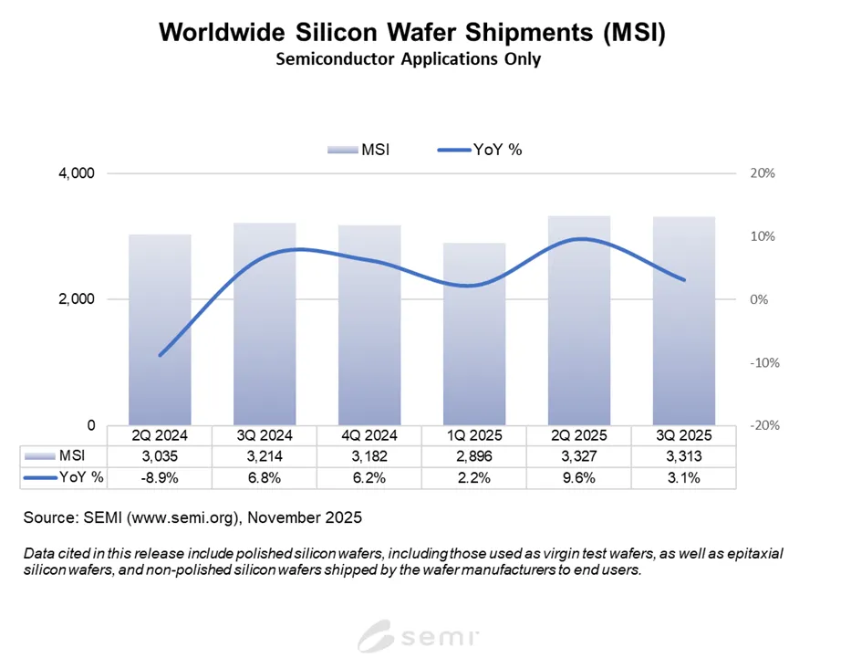
MILPITAS, Calif. — November 4, 2025 — The SEMI Silicon Manufacturers Group (SMG) reported today, in its quarterly analysis of the silicon wafer industry, that worldwide silicon wafer shipments increased 3.1% year-on-year to 3,313 million square inches (MSI) from the 3,214 MSI recorded during the same quarter of 2024. Sequentially, shipments slipped 0.4% quarter-over-quarter from the 3,327 MSI recorded during the second quarter of this year indicating softness in recovery particularly for epitaxial wafers slices. 

SEMI“January through September silicon shipments registered a significant year-on-year increase primarily driven by the growth of 300 mm shipments for advanced logic, cloud infrastructure, and memory demand,” said Lee Chungwei (李崇偉), Chairman of SEMI SMG and Vice President and Chief Auditor at GlobalWafers. “AI empowers significant investments expansion in advanced processes contributing to the wafer demand growth.”

Silicon wafers are the fundamental building material for the majority of semiconductors, which are vital components of all electronic devices. The highly engineered thin disks are produced in diameters of up to 300 mm and serve as the substrate material on which most semiconductors are fabricated.

The SMG is a sub-committee of the SEMI Electronic Materials Group (EMG) and is open to SEMI members involved in manufacturing polycrystalline silicon, monocrystalline silicon or silicon wafers (e.g., as cut, polished, epitaxial). The SMG facilitates collective efforts on issues related to the silicon industry, including the development of statistics about the silicon industry.

For more information, visit SEMI Worldwide Silicon Wafer Shipment Statistics.

About SEMI

SEMI® is the global industry association connecting over 3,000 member companies and 1.5 million professionals worldwide across the semiconductor and electronics design and manufacturing supply chain. We accelerate member collaboration on solutions to top industry challenges through Advocacy, Workforce Development, Sustainability, Supply Chain Management and other programs. Our SEMICON® expositions and events, technology communities, standards and market intelligence help advance our members’ business growth and innovations in design, devices, equipment, materials, services and software, enabling smarter, faster, more secure electronics. Visit www.semi.org, contact a regional office, and connect with SEMI on LinkedIn and X to learn more.


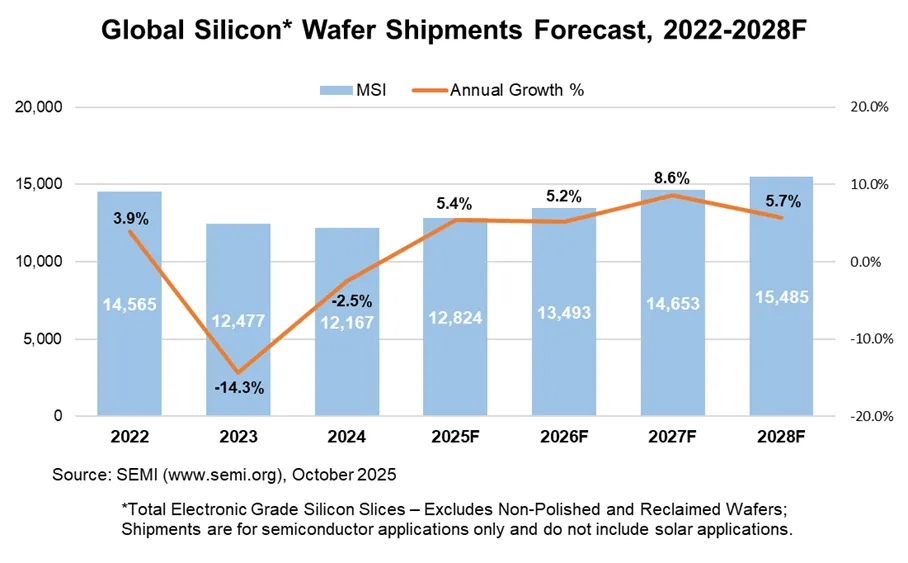
MILPITAS, Calif. ─ October 28, 2025 ─ Global shipments of silicon wafers are projected to increase 5.4% in 2025 to 12,824 million square inches (MSI) followed by steady growth through 2028 when the market is expected to reach a new industry record of 15,485 MSI, SEMI reported today in its annual silicon shipment forecast. 

SEMIIn 2025, the increase in silicon wafer shipments has been supported by strong AI-related growth, including advanced epitaxial wafers for leading edge logic devices and polished wafers for high bandwidth memory (HBM). Wafer shipments for non-AI applications, however, are just beginning to demonstrate a gradual recovery from the recent downcycle. The steady growth is expected to continue through 2028, driven by AI’s expanding compute footprint in data centers and at the edge.

Silicon wafers are the fundamental building material for the majority of semiconductors, which are vital components of all electronic devices. The highly engineered thin disks, produced in diameters of up to 300 mm, serve as the substrate material on which most semiconductor devices, or chips, are fabricated.

All data cited in this release include polished silicon wafers and epitaxial silicon wafers shipped by wafer manufacturers to end users. The data does not include non-polished or reclaimed wafers.

The annual silicon shipment forecast is developed based on input from the members of the Silicon Manufacturers Group (SMG). The SMG is a sub-committee of the SEMI Electronic Materials Group (EMG). This forecast reflects industry input gathered by SEMI and does not represent an official forecast of the SMG or any individual member company.  

For more information, please visit SEMI Worldwide Silicon Wafer Shipment Statistics, SEMI Market Data or contact [email protected].

About SEMI

SEMI® is the global industry association connecting over 3,000 member companies and 1.5 million professionals worldwide across the semiconductor and electronics design and manufacturing supply chain. We accelerate member collaboration on solutions to top industry challenges through Advocacy, Workforce Development, Sustainability, Supply Chain Management and other programs. Our SEMICON® expositions and events, technology communities, standards and market intelligence help advance our members’ business growth and innovations in design, devices, equipment, materials, services and software, enabling smarter, faster, more secure electronics. Visit www.semi.org, contact a regional office, and connect with SEMI on LinkedIn and X to learn more.


MILPITAS, Calif. – October 27, 2025 – SEMI, the industry association serving the global semiconductor and electronics design and manufacturing supply chain, today announced updates to the SEMI International Board of Directors. Tetsuro (Terry) Higashi, Chairman of the Board of Directors for Rapidus, has been elected and began his three-year term on the SEMI International Board.

The following six board members have been reelected and were announced during the SEMI annual membership meeting on October 8, 2025, at SEMICON West:

  • Tim Archer, President and CEO, Lam Research
  • Doris Hsu, Chairperson and CEO, GlobalWafers
  • Toshiki Kawai, Representative Director, President and CEO, Tokyo Electron
  • Jon Kemp, President, Electronics and Industrial, DuPont
  • Yong Han (YH) Lee, Chairman, Wonik
  • Sue Lin, Vice Chairman, Hermes Epitek

The 18 voting directors and 10 emeritus directors on the SEMI International Board represent companies from across the global microelectronics supply chain, positioning SEMI to best support innovation in all areas of the industry. 

SEMI directors are elected by the general membership as voting members of the Board and can serve a total of five, three-year terms.

About SEMI

SEMI® is the global industry association connecting over 3,000 member companies and 1.5 million professionals worldwide across the semiconductor and electronics design and manufacturing supply chain. We accelerate member collaboration on solutions to top industry challenges through Advocacy, Workforce Development, Sustainability, Supply Chain Management and other programs. Our SEMICON® expositions and events, technology communities, standards and market intelligence help advance our members’ business growth and innovations in design, devices, equipment, materials, services and software, enabling smarter, faster, more secure electronics. Visit www.semi.org, contact a regional office, and connect with SEMI on LinkedIn and X to learn more. 


MILPITAS, Calif. – October 23, 2025 – To help meet the growing demand for skilled workers in the U.S. semiconductor and microelectronics industry, the National Network for Microelectronics Education (NNME), operated by the SEMI Foundation, today announced the launch of ChipPath, a first-of-its-kind, AI-enabled career platform that connects individuals directly to real opportunities across the industry.

With over 90,000 live job postings and counting, ChipPath is already one of the most comprehensive semiconductor workforce tools in the country. Unlike traditional job boards, ChipPath autonomously scrapes and aggregates open positions from the websites of SEMI member companies, capturing tens of thousands of roles across the full microelectronics supply chain, from design and manufacturing to automation, facilities, and materials.

“ChipPath is more than a job board, it’s a bridge to opportunity,” said Shari Liss, Vice President of Workforce Development and Initiatives at SEMI. “It’s a movement to make the semiconductor workforce accessible to all Americans. This platform opens doors for students, veterans, career changers, and seasoned engineers, helping to see themselves in this industry and take real, actionable steps toward building their future in it.”

Building the Bridge Between Talent and Opportunity

The semiconductor industry is expanding at record speed, yet many potential job seekers don’t know how to start an industry career. ChipPath bridges that gap by helping users explore, prepare, and connect through an integrated set of tools designed specifically for semiconductor careers.

The platform includes four powerful components:

  1. Smart Resume Builder: Creates professional, industry-aligned resumes in minutes using AI-driven prompts that highlight relevant skills, certifications, and experience.
  2. Career Mapping & Exploration: Helps users discover the breadth of opportunities in semiconductors and visualize clear pathways to advancement.
  3. Training & Development Resources: Connects learners to certificate programs, apprenticeships, and degree pathways offered by NNME partners across the country.
  4. Live Job Openings Nationwide: Features over 90,000 active roles scraped directly from SEMI member company websites, providing a real-time view of the industry’s hiring landscape.

“For too long, semiconductor careers have been somewhat invisible, seemed out of reach or hard to navigate,” said Michelle Williams, Executive Director of the SEMI Foundation. “ChipPath changes that. It illuminates opportunities, empowers people to see where they fit, and gives them the tools to get there. No gatekeeping, no guesswork.”

Next Up: Employer Dashboard Launching in 2026

The NNME and SEMI Foundation are already developing the next phase of ChipPath: a robust Employer Dashboard set to debut in early 2026. This feature will enable companies to curate and prioritize the skills and qualifications most important to their workforce needs, search and connect directly with job seekers, and gain data-driven insights into national workforce trends.

The platform already operates autonomously, capturing tens of thousands of opportunities in real time. The next update will add a powerful new layer of interactivity, allowing employers to engage directly with candidates and shape the future of their talent pipelines.

About the SEMI Foundation

The SEMI Foundation’s mission is to support economic opportunity for workers and the sustained growth of the microelectronics industry through creating pathways and opportunities for job seekers and tools and systems for semiconductor companies to attract, develop, retain, and advance a diverse and skilled workforce. Visit the SEMI Foundation online to learn more, and follow the SEMI Foundation on LinkedIn.

About the National Network for Microelectronics Education (NNME)

The National Network for Microelectronics Education (NNME), operated by the SEMI Foundation, is setting America’s gold standard for workforce development in microelectronics. Our mission is clear: to deliver employer-aligned curriculum and modern, work-based learning that prepares all Americans for high-quality careers that advance U.S. innovation and prosperity. Visit www.nnme.org to learn more. 

About SEMI

SEMI® is the global industry association connecting over 3,000 member companies and 1.5 million professionals worldwide across the semiconductor and electronics design and manufacturing supply chain. We accelerate member collaboration on solutions to top industry challenges through Advocacy, Workforce Development, Sustainability, Supply Chain Management and other programs. Our SEMICON® expositions and events, technology communities, standards and market intelligence help advance our members’ business growth and innovations in design, devices, equipment, materials, services and software, enabling smarter, faster, more secure electronics. Visit www.semi.org, contact a regional office, and connect with SEMI on LinkedIn and X to learn more. 


MILPITAS, Calif. – October 21, 2025 – SEMI, the industry association serving the global semiconductor and electronics design and manufacturing supply chain, today announced the recipients of the North America Standards International Awards, presented on October 7 at SEMICON West 2025 in Phoenix, Arizona. Leaders from across the microelectronics industry were recognized for their outstanding contributions to the SEMI Standards Program that guide today’s semiconductor manufacturing processes. Award winners received accolades in one of five distinct categories. 

The Merit Award

The 2025 Merit Award was presented to five individuals who made significant contributions to the semiconductor industry through the SEMI Standards Program, leading projects to successful completion at the task force level. 

Dave Dunne of Applied Materials is an active member of the North America Fab & Equipment Computing and Device Security (CDS) Task Force. Dunne was instrumental in developing two new SEMI cybersecurity standards, SEMI E191 and SEMI E191.1. These standards outline the required status information for each computing device to help factories evaluate their cybersecurity risk. Dunne also participated in creating SEMI cybersecurity standards E187 and E188, which provide crucial cybersecurity feedback from the equipment supplier perspective. 

Kirsten Smith and Tommaso Orzali of UCT/ChemTrace and ASML, respectively, worked closely with the Critical Chamber Components (CCC) Task Force to create SEMI E194 and SEMI E195. Both standards experienced multiple revisions before they were finally published earlier this year to address CCC contamination. Smith and Orzali are now leading the development of a new overarching document that offers guidance on the best CCC assessment methods across multiple applications. 

Dr. Tyler Harrison and Dr. Mary Ann Maher of Teledyne MEMS and SoftMEMS, respectively, were instrumental in advancing SEMI MS15 to completion after an arduous year of revisions. SEMI MS15 emphasizes best practices to help MEMS development teams meet performance, cost, quality, and time-to-market goals. This crucial standard helps reduce risks, promote efficiency, and accelerate commercialization in the MEMS industry. 

The Leadership Award

The Leadership Award is earned by those who have strengthened the SEMI Standards program through member recruitment, training, and mentoring. These individuals have been essential in transforming new volunteers into positive committee contributors by guiding them through the standardization process flow. 

Michael Potts of Arcadis is a member of the North America Regional Standards Committee (NARSC), chairs the SEMI Standards Facilities North America Global Technical Committee, and led the Building Information Modeling (BIM) for Semiconductor Capital Task Force, now known as the Manufacturing Equipment Installation Task Force. Potts was critical for developing the newly published SEMI F122, which offers a standardized format for creating 3D BIMs of semiconductor equipment. This standard aims to help manufacturers utilize digital twins to boost efficiency and reduce costs.

David Kandiyeli of KINETICS Equipment Solutions Group is a member of the NARSC and co-chairs the SEMI Standards Liquid Chemicals North America Global Technical Committee. Kandiyeli has written and revised many fundamental standards, including SEMI F31 for bulk chemical distribution systems, SEMI F39 for chemical blending systems, and SEMI F41 for qualification of bulk chemical distribution systems, among many others. Kandiyeli has also contributed heavily to several slurry standards, most notably SEMI C96, SEMI C99, and SEMI C101. 

Per Nelson of Daikin America is a member of the NARSC, co-chairs the SEMI Standards Liquid Chemicals North America Global Technical Committee, and co-leads the High Purity Polymer Materials and Components Task Force. He actively participated in writing and revising core standards like SEMI C69 and SEMI C90, alongside other fundamental chemical standards. 

These leaders have the ability to build consensus among stakeholders with differing perspectives demonstrating their exceptional leadership, patience, and commitment to advancing the SEMI Standards program.

The Honor Award

The Honor Award is presented to individuals who have demonstrated long-term dedication to advancing SEMI Standards. The following industry leaders have served the program consistently over several years. 

Steve Martell of Nordson Test & Inspection Americas has participated in the SEMI Standards Program for more than 20 years, when the first MEMS standards were being authored. Martell’s extensive experience in the program has helped drive many widely used standards to completion, and he remains a key force in pushing topics through the SEMI Standards process. He is a member of the NARSC, chairs the MEMS/NEMS North America Global Technical Committee, and regularly acts as chair for the 3D Packaging & Integration (3DP&I) North America Committee. 

Lucian Girlea of Nikon Precision has been a consistent and active participant in various Environmental, Health, and Safety (EH&S) standards task forces. He currently serves as a leader for the Manufacturing Equipment Safety Subcommittee (MESSC), a position he has held for over six years. A core focus area for the MESSC is safety interlocks, where Girlea recognized the need for greater harmonization and consistent terminology. In response to this, he launched the SEMI S2 Safety Interlock Task Force, which later became the SEMI S2 Major Revision Task Force. 

Dave Huntley of PDF Solutions has led the Single Device Traceability (SDT) Task Force for over five years. He was instrumental in the development of SEMI T26, a new standard published in September 2025, which helps increase supply chain transparency by utilizing ledgers to track the status of various equipment parts.

Corporate Device Member Award

The Corporate Device Member Award honors those who act as corporate representatives for the SEMI Standards Program from the device manufacturer side. Individuals who receive this award are participants from the user community who garner support for SEMI Standards.

Stefan Radloff of Intel has been participating in the SEMI Standards Program for over 28 years. He leads the Film Frame FOUP Task Force and co-leads the Next Generation Assembly/Test Material Handling Japan Task Force. Radloff has consistently driven results through his extensive industry experience, spearheading the development of several standards in the SEMI Equipment Automation Software & Hardware (E) volume. Radloff has supported core standards like SEMI E84 for carrier handoff, as well as recent advanced packaging standards like SEMI E193 that specify physical dimensions for 300mm Film Frame FOUPs. 

Technical Editor Appreciation Award

The Technical Editor Appreciation Award recognizes technologists with highly developed language skills. Individuals who earn this award are adept at translating complex technical information into clear and precise expression.             

Dr. Alissa M. Fitzgerald of A.M. Fitzgerald & Associates contributed her technical expertise to help drive the publication of SEMI MS15 for MEMS manufacturing readiness. Fitzgerald also participated in other MEMS industry standards, including SEMI MS12 and SEMI MS13. Her skill in wording these complex technical documents significantly improved their clarity and quality. Fitzgerald’s unique combination of both technical understanding and superb writing abilities exemplifies the qualities of the Technical Editor Appreciation Award. 

For more information, visit the SEMI International Standards webpage. 

About SEMI

SEMI® is the global industry association connecting over 3,000 member companies and 1.5 million professionals worldwide across the semiconductor and electronics design and manufacturing supply chain. We accelerate member collaboration on solutions to top industry challenges through Advocacy, Workforce Development, Sustainability, Supply Chain Management and other programs. Our SEMICON® expositions and events, technology communities, standards and market intelligence help advance our members’ business growth and innovations in design, devices, equipment, materials, services and software, enabling smarter, faster, more secure electronics. Visit www.semi.org, contact a regional office, and connect with SEMI on LinkedIn and X to learn more. 


TOKYO – October 21, 2025 – SEMICON Japan 2025, the largest gathering of leaders from the microelectronics manufacturing supply chain in Japan, will bring together more than 1,200 exhibitors showcasing semiconductor solutions from December 17-19 at Tokyo Big Sight. The event will showcase the latest innovations and trends in the global semiconductor industry through a range of exhibitions, seminars, and forums. Key topics will include advancements across the design and manufacturing supply chain, emerging technologies such as quantum computing, photonics-electronics convergence, advanced packaging, as well as AI, gaming, robotics, mobility, aerospace, and medical applications. Registration is open. 

SEMICON JapanTwo new summits will be held, including the AI x Sustainability x Semiconductor Summit tied to this year’s event theme, and the Metrology and Inspection Summit (MIS). Additionally, SEMICON Japan will feature concurrent events Advanced Packaging and Chiplet Summit (APCS), which will bring together top players in the semiconductor packaging and board assembly fields, as well as the Advanced Design Innovation Summit (ADIS), which will focus on new-generation semiconductor design and verification.

In conjunction with SEMICON Japan, the Strategic Materials Conference (SMC) will be held for the first time in Japan on December 16, convening executives to discuss and learn about the latest technologies and market trends in AI and advanced semiconductors. 

SEMICON Japan 2025 Featured Speakers 

  • Mukesh Khare, GM and Vice President of Hybrid Cloud Research at IBM Semiconductors
  • Scott DeBoer, Executive Vice President of Micron Technology
  • Akiko Kudo, Representative Director and Executive Vice President of NTT Docomo Business
  • Toshiki Kawai, President and CEO of Tokyo Electron

Additional Conference Highlights

  • Market and Advocacy: Experts from various fields, including government officials, researchers, and analysts, will discuss the latest semiconductor market trends with a focus on business. Sessions include the SEMI Market Forum, Semiconductor Materials Forum and Bulls & Bears featuring Japan’s top securities analysts.
  • Special Events and Guests: Guests active in a variety of fields will add color to the event, including Narita Yusuke’s Passion Lab, where economist Narita Yusuke and 100 students will discuss the future of digitalization, and Monozukuri Taro Presents the Semiconductor and Robotics Industry, a seminar by manufacturing YouTuber Monozukuri Taro.
  • Workforce Development: These programs support early career professionals and talent development who will lead the industry in the future.
    • Thursday Wakamono Night, a forum highlighting a new project to engage students and young employees.
      • 58 semiconductor-related companies will gather together at the semiconductor industry research event Mirai College.
      • The College of Technology exhibits technology and research results of young students.
      • Academia exhibition of semiconductor research results by university laboratories, and the Academia Award recognizing achievements.
      • Women in Business panel discussion.
  • Technology Events: These sessions allow attendees to experience the latest technology and learn from entertainment to specialized knowledge.
    • Two new projects include: The Game, which uses a card game as teaching material for SoC design, and Circuit Design, a competition aimed at students who will be responsible for the future of semiconductor design.
    • In addition, the Semiconductors & e-Sports section will introduce the intersection between the latest games and semiconductor technology and will also feature an exhibition by professional players.

SEMICON Japan is offering its first-ever early bird discount. Attendees who register early for paid seminars get 20% off the participation fee.

This year, early bird discounts on premium seminars will be provided (fees apply). Aimed at professionals in the semiconductor industry, the courses offer a wide range of topics, from technology, market and regulatory compliance to training young engineers, providing knowledge that is directly linked to practical work. To allow as many people as possible to participate, limited early bird discounts will be offered for applications submitted by Friday, October 31, 2025.

Due to partial renovations to the Tokyo Big Sight East Exhibition Hall, the event will be held in Halls 4-6 of the East Exhibition Hall, the West and South Exhibition Halls, and the Conference Tower. 

To participate in the SEMICON Japan 2025 exhibition, seminars, and events, and for advance registration, visit the SEMICON Japan website.

About SEMICON Japan 2025

SEMICON Japan 2025 is an event held to deepen insights into the latest trends and innovative technologies related to sustainability, supply chain management, human resource development, and other key industry issues. It invites thought leaders from the electronics design and manufacturing ecosystem, academia, and government to deliver keynote speeches and business seminars. The 2025 event will mark the 49th time the event is held in Japan. Since its inception in 1977, the event has introduced cutting-edge semiconductor technology and its trends to the Japanese public. In recent years, the event has focused on semiconductors as the core of cutting-edge technology supporting the digital transformation era, covering a wide range of topics unparalleled in Japan, from semiconductor manufacturing technologies, equipment, and materials to application areas such as automobiles, IoT devices, and medical devices.

About SEMI

SEMI® is the global industry association connecting over 3,000 member companies and 1.5 million professionals worldwide across the semiconductor and electronics design and manufacturing supply chain. We accelerate member collaboration on solutions to top industry challenges through Advocacy, Workforce Development, Sustainability, Supply Chain Management and other programs. Our SEMICON® expositions and events, technology communities, standards and market intelligence help advance our members’ business growth and innovations in design, devices, equipment, materials, services and software, enabling smarter, faster, more secure electronics. Visit www.semi.org, contact a regional office, and connect with SEMI on LinkedIn and X to learn more.