downloadGroupGroupnoun_press release_995423_000000 copyGroupnoun_Feed_96767_000000Group 19noun_pictures_1817522_000000Member company iconResource item iconStore item iconGroup 19Group 19noun_Photo_2085192_000000 Copynoun_presentation_2096081_000000Group 19Group Copy 7noun_webinar_692730_000000Path
Skip to main content
Default Banner Image

SEMI Press Release

ID
semi-press-release

MILPITAS, Calif. – August 27, 2026 – SEMI, the industry association advancing the global semiconductor and electronics design and manufacturing supply chain, today announced keynotes and program highlights for this year’s SEMICON® West on October 13–15 at the Moscone Center in San Francisco. Registration is open.

As the semiconductor industry enters a new era of unprecedented growth, SEMICON West will bring together leaders from across the global microelectronics ecosystem to address the technologies, investments and industry priorities shaping the path from $1 trillion toward $2 trillion in annual semiconductor revenue. Programming will span advanced manufacturing, AI and next-generation computing, supply chain resilience, sustainability, workforce development, and the continued expansion of semiconductor manufacturing infrastructure.

“Clearing the industry’s $1 trillion annual revenue milestone almost four years ahead of earlier projections is evidence of today’s remarkable demand for semiconductors, but growth at this scale presents new challenges the industry must tackle together,” said Joe Stockunas, President of SEMI Americas. “The 2026 program will celebrate this monumental achievement while strategizing for the $2 trillion and beyond future. As we scale beyond traditional Moore’s Law, expand U.S. manufacturing infrastructure, and build the future workforce, SEMICON West will convene the industry to prepare for a new wave innovation to transform tomorrow.” 

SEMICON West Program Highlights:

CEO Summit Keynotes 

The CEO Summit Keynotes will feature industry executives and government leaders sharing insights on global trends and challenges reshaping the semiconductor ecosystem. CEO Summit Keynote sessions will run from Tuesday, October 13 through Thursday, October 15 from 8:30-11 a.m. and will include the following speakers, with more to be announced. Join us on Tuesday morning at the CEO Summit to open the exhibition and celebrate the industry surpassing $1 trillion in annual revenue. 

  • Sassine Ghazi: President and CEO, Synopsys – with fireside chat host Ed Sperling: Editor-in-Chief, Semiconductor Engineering 
  • David Jarzynka: CEO, Brooks Automation
  • Thomas Sonderman: President and CEO, SkyWater Technology 
  • Justin Murrill: Chief Sustainability Officer, AMD 
  • Surésh Rajaraman: Executive Vice President and CTO, EMD Electronics
  • Scott Gatzemeier: Corporate Vice President, Micron 
  • Timothy Costa: Vice President and General Manager, Industrial and Computational Engineering, NVIDIA
  • Lalitha Immaneni, Vice President, Semiconductor Research and Development, Intel
  • Bill Frauenhofer: Executive Director of Semiconductor Investment and Innovation, U.S. Department of Commerce 
  • Erwin Gianchandani, PhD: Assistant Director for Technology, Innovation and Partnerships, National Science Foundation, NSF 
  • Jacob Helberg: Under Secretary of State for Economic Affairs, U.S. Department of State
  • Kevin Younis: Chief Operating Officer and Executive Deputy Commissioner, Empire State Development  
     

Executive Panels 

Geopolitics: Subject matter experts will examine the evolving geopolitical landscape impacting the semiconductor industry, including changing government policies, strategic trade agreements, and emerging supply chain risks.  This session will be held on October 13 from 1:30-2:30 p.m. Featured speakers will be announced. 

Transforming Tomorrow: Collaboration, Innovation, and Talent Shaping the Future of Semiconductor Manufacturing: Moderated by David Anderson, President of NY CREATES, this executive panel will explore how innovation, ecosystem collaboration, and workforce development are driving the next generation of semiconductor manufacturing. Industry leaders will share insights on AI-enabled production, sustainable growth, and the talent needed to power the industry's future. Featured speakers will be announced for this session to be held on October 14 from 10-10:55 a.m.

Supply Chain: On October 14 from 1-2 p.m., senior executives will discuss strategies for building more resilient and responsive semiconductor supply chains, including enhanced visibility across regions and manufacturing partners, collaborative approaches to managing volatility, and emerging ecosystem models. Featured speakers will be announced.

Market Intelligence and Industry Outlook 

Bulls and Bears: As AI-driven demand accelerates investment in semiconductor manufacturing capacity, industry and financial experts will examine the opportunities and risks shaping the semiconductor capital equipment sector, including valuation trends, capital requirements, growth sustainability, and future market dynamics.  This panel will be held on October 14 from 2-3 p.m. 

  • Stacy A. Ragson: Managing Director and Analyst, Bernstein Research
  • C.J. Muse: Senior Managing Director, Cantor Fitzgerald 
  • Franklin Keller: Founder and Chief Investment Officer, Talos Eurisko Asset Management
  • Ryan Grimshaw: Portfolio Manager, Summit Partners
  • Moderated by Claire McAdams: Founder and CEO, Headgate Partners

SEMI Market Symposium: This session will provide expert analysis on key technology and market trends, including AI, global economic shifts, and geopolitical forces shaping trade and industry investments. SEMI Market Symposium will take place before the conference on Monday, October 12 from 1-5 p.m. Featured speakers will be announced.

Additional Programs Feature Technologies Shaping What Comes Next and Networking Opportunities

  • Focused Forums: Expert-led forums covering key industry priorities on Cybersecurity, Advanced Manufacturing, Smart Manufacturing, Smart Mobility, and Sustainability. 
  • Technical Programs: The Advanced Packaging & Heterogenous Integration (APHI) Summit; Test Vision Symposium; Materials & Advanced Substrates, Semiconductor Components, Instrumentation & Subsystems (SCIS); and additional sessions addressing critical microelectronics technologies and innovations.
  • Future Technology Sessions: Insights into emerging technologies shaping the future, including Future of AI Computing, Quantum Computing, Photonics, Flexible Hybrid Electronics, Smart MedTech, and other technologies needed to sustain AI infrastructure growth and enable edge AI.
  • Supply Chain Sessions: Discussions on semiconductor manufacturing expansion, workforce and infrastructure development, supply chain resilience, and the digital technologies transforming global supply networks.
  • Bridging Design and Manufacturing with AI: Design houses, foundries, systems companies and equipment makers will present new strategies on how AI can enable bespoke design, shorten design-to-silicon cycles, and accelerate semiconductor manufacturing through smarter collaboration, automation, and data-driven decision-making. 
  • MEMS & Sensors: Session highlighting advances in sensing technologies and microsystems that enable next-generation applications across automotive, industrial, healthcare, consumer, and connected devices.
  • SEMI Workforce Development Pavilion: A dedicated hub connecting job seekers with employers, with industry speakers and workforce initiatives aimed at strengthening the semiconductor industry talent pipeline. 
  • SEMI U: Tailored semiconductor training courses to advance attendees’ knowledge and skills.
  • SEMI Women's Network: The program includes focused conversations and networking experiences including a luncheon centered on advancing women in semiconductors.
  • SEMICON WestFest: An Oktoberfest-style celebration with live music, Bavarian bites, and interactive experiences to bring attendees together.
  • Networking Receptions: Ample opportunities to strengthen relationships and forge new connections long after the show floor closes each day.

Frequently Asked Questions 

How do I register for SEMICON West? 

SEMICON West offers three registration tiers. Pricing varies depending on SEMI membership status. 

  • The Expo Plus Pass grants access to all exhibits, keynote presentations, and sessions taking place on the expo floor stages. 
  • The Thought Leadership Pass offers expanded access to industry discussions, including SEMI’s Market Symposium, Cybersecurity Forum, Test Vision Symposium, Advanced Packaging & Heterogeneous Integration (APHI) Summit and Reception, and the Future of AI and Quantum Computing.
  • The All-In Pass is SEMICON West’s most complete pass, with VIP lounge access and badge pickup and daily lunch.

Learn more about registration options. 

Who exhibits at SEMICON West? 

Over 734 companies and organizations exhibit at SEMICON West each year, including semiconductor equipment makers, material suppliers, supply chain leaders, and government bodies from around the world. This year’s SEMICON will feature more than 1,500 booths and draw over 35,000 attendees. Although the 2026 exhibit floor is sold out, discover the benefits of exhibiting at SEMICON West in 2027. 

Where will SEMICON West take place next year? 

SEMI recently announced a new annual schedule for future SEMICON West events. Starting in 2027, SEMICON West will be held during spring at the Phoenix Convention Center in Phoenix, Arizona. Next year’s event will take place from March 30-April 1, 2027. 

This time and location change represents a strategic transition to provide attendees and exhibitors with greater flexibility to attend SEMICON events around the world. SEMICON West will remain in Phoenix until 2029.

Connect With SEMI 

For more information, please visit the SEMICON West 2026 website. For press interested in attending SEMICON West 2026, please visit our Virtual Press Office and contact Samer Bahou at [email protected]. 

Follow SEMI 

About SEMI

SEMI® is the global industry association connecting over 4,000 companies and 1.5 million professionals worldwide across the semiconductor and electronics design and manufacturing supply chain. We accelerate member collaboration on solutions to top industry challenges through Advocacy, Workforce Development, Sustainability, Supply Chain Management and other programs. Our SEMICON® expositions and events, technology communities, standards and market intelligence help advance our members’ business growth and innovations in design, devices, equipment, materials, services and software, enabling smarter, faster, more secure electronics. Visit www.semi.org, contact a regional office, and connect with SEMI on LinkedIn and X to learn more. 

 

BRUSSELS – September 14, 2026 – SEMI , the industry association advancing the global semiconductor and electronics design and manufacturing supply chain, today announced it has joined the ReSiLient project consortium to help fortify Europe’s semiconductor ecosystem and advance global supply chain resilience. Kicking off in 2026, the project aims to tackle Europe’s critical dependence on imported silicon (Si) and silicon carbide (SiC) raw materials. 

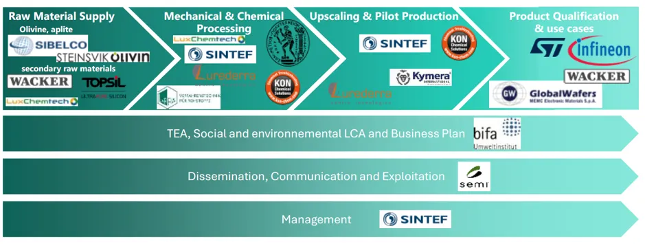
As part of SEMI’s participation, SEMI Europe will serve as lead partner for Work Package 8 (WP8), Social Acceptance, Dissemination, Communication and Standardization. Co-funded by the European Union under the Horizon Europe program (Grant Agreement No. 101294649), the ReSiLient project — Innovative Primary Substitution and Secondary Valorisation Routes for Europe’s Silicon and Silicon Carbide Semiconductor Raw Material Value Chains — is a 48-month, €9.57 million Innovation Action bringing together 18 partners from across 9 European countries.

“Securing Europe’s access to silicon and silicon carbide is no longer simply a materials challenge—it is a strategic industrial imperative,” said Laith Altimime, President, SEMI Europe. “ReSiLient tackles the critical raw-material bottlenecks at the very foundation of Europe’s semiconductor and power-device industries. SEMI Europe is committed to ensuring these results reach the industrial stakeholders who can turn them into action. By strengthening the resilience of Europe’s raw-material supply, ReSiLient will help reinforce the Europe’s semiconductor ecosystem, competitiveness, and global leadership.”
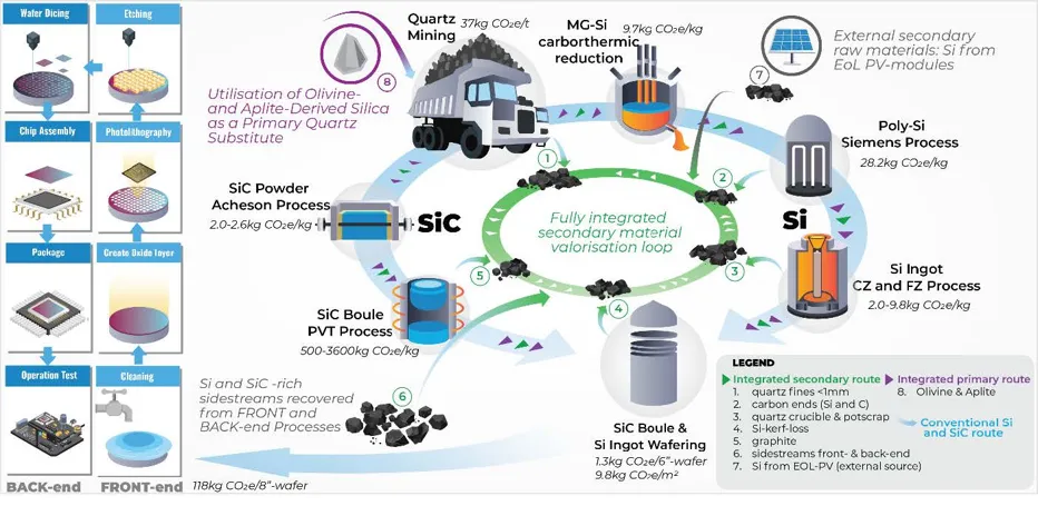
ReSiLient Concept (Source: ReSiLient Consortium)

The project addresses four strategic objectives:

  1. Supply chain resilience — Map critical dependencies across the Si and SiC value chains, validate domestic and secondary feedstocks including olivine, aplite and Si-rich industrial waste streams, and align new production routes with the Critical Raw Materials Act, European Chips Act, Net-Zero Industry Act and EU Emissions Trading System.
  2. Sustainable production at scale — Develop and demonstrate two integrated production routes: a primary route based on domestic mineral sources, and a secondary route based on industrial by-products and waste streams, using hydrometallurgical leaching, agglomeration, hydrogen plasma refining and carbothermic conversion to deliver metallurgical-grade silicon and high-purity silicon carbide at pilot scale.
  3. Semiconductor qualification — Validate the purity and performance of project-produced Si, MG-Si and SiC for real semiconductor manufacturing, including Czochralski crystal growth and SiC boule production, benchmarked against commercial feedstock by end users STMicroelectronics Silicon Carbide AB and Infineon Technologies.
  4. Competitiveness and exploitation — Benchmark both production chains against conventional baselines on cost, carbon footprint and supply security, and define clear commercial pathways, Intellectual Property Rights (IPR) frameworks and regulatory compliance strategies for scale-up.

 Value Chain

The ReSiLient consortium spans the full microelectronics value chain:

Sintef, Luxchemtech Gmbh, Fiven Norge, Bifa Umweltinstitut Gmbh, Ethnicon, Metsovion Polytechnion, Steinsvik Olivine As, Konlechner David, Wacker Chemie Ag, Semi Europe Gmbh, L'urederra, Fundacion Para El Desarrollo Tecnoles, Stmicroelectronics Silicon Carbide Ab, Infineon Technologies Ag, Chemconserve Bv, Topsil Globalwafers As, Memc Electronic Materials Spa, Scr-Sibelco Nv, Infineon Technologies Dresden Ag & Co. Kg De, Uvr-Fia Verfahrensentwicklung Umweltschutzec De.

As lead of WP8, SEMI Europe will drive stakeholder engagement across at least 10 European member states, coordinate communication activities anchored around key industry events including SEMICON Europa, develop standards and chair the project's external Technical Advisory Group. 

For more information about ReSiLient, visit www.resilient-semiconductors.eu or get involved by contacting [email protected].   

About SEMI 

SEMI® is the global industry association connecting over 4,000 companies and 1.5 million professionals worldwide across the semiconductor and electronics design and manufacturing supply chain. We accelerate member collaboration on solutions to top industry challenges through Advocacy, Workforce Development, Sustainability, Supply Chain Management, and other programs. Our SEMICON® expositions and events, technology communities, standards, and market intelligence help advance our members’ business growth and innovations in design, devices, equipment, materials, services, and software, enabling smarter, faster, more secure electronics. Visit www.semi.org, contact a regional office, and connect with SEMI on LinkedIn and X to learn more.

~SEMI Event is India's Largest for the Global Semiconductor Ecosystem Bringing Together 500+ Exhibitors, 243 International companies, 150+ Speakers and Delegates from 40+ Countries~

NEW DELHI, AUGUST 18, 2026:  India's semiconductor ambitions are entering a decisive new phase. Having successfully attracted landmark investments under the Ministry of Electronics & Information Technology (MeitY) Semicon India Programme, the country is now accelerating towards building a complete and globally competitive semiconductor ecosystem spanning design, manufacturing, packaging, materials, equipment, electronics systems, research, innovation and talent development.

Reflecting this transformation, SEMI and the India Semiconductor Mission (ISM) today announced that Hon'ble Prime Minister Shri Narendra Modi will inaugurate SEMICON India 2026 on 17 September 2026 at Yashobhoomi (India International Convention and Expo Centre), New Delhi.

Hosted by SEMI and jointly organised under the aegis of the ISM, MeitY, and Government of India, this edition of SEMICON India will be held from 17–19 September 2026 under the theme: "Transform Tomorrow: Silicon to Systems – Building the Ecosystem."

Shri S. Krishnan, Secretary, Ministry of Electronics & Information Technology (MeitY), said "The Government of India has given clear indication towards the importance and significance of the Semiconductor Sector with its progressive policies and extended support. The sense of participation around the SEMICON India Conference and Exhibition has grown significantly each year. This year it is particularly significant for two reasons. Firstly, we are convening this event against the backdrop of the on-ground success of Semicon India Programme, with 03 of the 12 semiconductor projects approved under Semicon 1.0, having commenced commercial production. Secondly, the announcement of the next phase i.e. Semicon 2.0 with 06 major pillars, which further strengthens India’s commitment to build a robust and resilient semiconductor ecosystem."

Transform Tomorrow unites SEMI’s eight SEMICON events worldwide, from Taiwan and Japan to the United States and Europe. It reflects a single conviction: semiconductors are the foundation of every transformative technology. Through SEMICON India 2026, SEMI carries that global vision to one of the industry’s most promising markets.

Mr. Ajit Manocha, President & CEO, SEMI, said: "SEMI has empowered the rise of semiconductor hubs around the world for more than five decades, and India is well positioned to thrive with its blend of speed, ambition, talent and long-term vision. Through SEMICON India 2026, SEMI brings the collective strength of its global network to India’s journey. India’s opportunity is not simply to join the global supply chain, but to become integral to it. That is the ambition SEMICON India 2026 exists to accelerate."

The event has evolved into India's flagship global semiconductor platform and the annual meeting point for the world's semiconductor ecosystem to engage with India's rapidly expanding opportunities. Bringing together policymakers, global technology leaders, semiconductor manufacturers, equipment and materials suppliers, electronics companies, startups, academia, investors and students, SEMICON India has become a critical platform for partnerships, investments, innovation and talent development.

Shri Amitesh Kumar Sinha, CEO, India Semiconductor Mission (ISM), said, "SEMICON India 2026 is an opportunity to bring together representatives from countries and companies across the world, Indian companies that have been approved to set up manufacturing in India, and companies exploring opportunities in the country. It also brings together leaders and policymakers from the Central and State Government, along with supply-chain partners looking to support semiconductor design and manufacturing in India. Additionally, the global semiconductor requirement is expected to increase from around $1 trillion to $2 trillion, while India’s semiconductor requirement is also expected to grow from around $100 billion to $200 billion. Also, the conference will cover a wide range of themes across the semiconductor and electronics ecosystem including a dedicated session on ‘Women Empowerment & Leadership’."

Building upon the momentum of MeitY’s Semicon India Programme and recently launched Semicon 2.0, this year's edition of SEMICON India reflects the country's transition from attracting investments to enabling a fully integrated semiconductor ecosystem. The event aligns with the six strategic pillars of Semicon 2.0—Design of Chips, Machines and materials, Setting up more fabs, Further strengthening of the ATMP/OSAT industry, Research and Development and Talent Development —reinforcing India's vision of becoming a trusted global partner across the semiconductor value chain.

Mr. Ashok Chandak, President, SEMI India & IESA, said, SEMICON India 2026, with its theme 'Silicon to Systems – Building the Ecosystem,' reflects India's evolution towards creating a comprehensive and globally competitive semiconductor value chain. The remarkable global and Indian corporates interest in this year's event is a testament to the confidence that industry leaders place in India's semiconductor journey. SEMICON India has become the annual convergence point where industry leaders, policymakers, researchers, startups and investors come together, collaborations take shape, partnerships are forged, and the next phase of India's semiconductor growth is accelerated. The introduction of the new 'Sand to Silicon to Systems' Value Chain Experience this year demonstrates how India is progressing from building credibility to demonstrating capability, while showcasing the country's expanding strengths across the entire semiconductor ecosystem."

Registration for SEMICON India 2026 is now open at www.semiconindia.org

About SEMICON India

SEMICON India is India's premier semiconductor conference and exhibition jointly organised by the India Semiconductor Mission (ISM), Ministry of Electronics & Information Technology (MeitY), Government of India, and SEMI. It serves as the country's flagship platform for bringing together the global semiconductor and electronics ecosystem to advance collaboration, innovation, manufacturing, investments and talent development, while supporting India's vision of becoming a trusted global hub for semiconductor and electronics manufacturing.

About SEMI

SEMI® is the global industry association connecting over 4,000 companies and 1.5 million professionals worldwide across the semiconductor and electronics design and manufacturing supply chain. We accelerate member collaboration on solutions to top industry challenges through Advocacy, Workforce Development, Sustainability, Supply Chain Management and other programs. Our SEMICON® expositions and events, technology communities, standards and market intelligence help advance our members’ business growth and innovations in design, devices, equipment, materials, services and software, enabling smarter, faster, more secure electronics. Visit www.semi.org, contact a regional office, and connect with SEMI on LinkedIn and X to learn more.

MEDIA CONTACTS

Somdatta Sengupta, Consocia Advisory; Phone: 91-8861822111; Email: [email protected]

ANNEXURE – EVENT DETAILS 

Experiencing India's Semiconductor Value Chain

A defining highlight of SEMICON India 2026 will be the launch of the "Value Chain Experience"—an immersive exhibition journey that, for the first time, showcases India's complete "Sand to Silicon to Systems" ecosystem.

Visitors will experience the semiconductor value chain in its natural sequence, demonstrating how India's capabilities are expanding across every critical segment—from chip design to advanced manufacturing and electronics systems.

The exhibition has been reimagined into dedicated ecosystem zones covering:

  • Semiconductor Design & IP
  • Wafer Fabrication & Assembly and Test
  • Infrastructure & Utilities
  • Machines, Materials, Specialty Chemicals & Industrial Gases
  • Packaging & Advanced Packaging
  • Compound Semiconductors & Display Technologies
  • Electronics Components & Systems Manufacturing
  • AI, High-Performance Computing & Quantum Technologies
  • Country Pavilions
  • State Government Pavilions

The Value Chain Experience symbolises India's evolution from individual investment announcements to building an integrated, resilient and globally competitive semiconductor ecosystem.

Largest Edition Since Launch

SEMICON India 2026 is projected to be the largest edition since its inception, expanding nearly 30% over the previous edition. In just two years, it has become one of the fastest-growing events in SEMI’s global SEMICON portfolio.

The event will feature:

  • 500+ exhibitors representing the complete global semiconductor and electronics ecosystem
  • 243 International companies participation
  • 150+ internationally renowned speakers
  • Delegates from over 40 countries
  • 15,000+ square metres of exhibition space
  • 6 Country Roundtables
  • 10 State Government Pavilions
  • Dedicated conference tracks covering semiconductor manufacturing, advanced packaging, electronic components and systems, AI, display technologies, supply chain resilience, sustainability, startup innovation, women leadership forum and workforce development.
  • Startup Pavilion and Innovation Showcase
  • Startup Pitch Competition
  • Student Hackathon
  • Workforce Development Pavilion

The conference programme will include visionary keynotes, policy dialogues, executive panel discussions, fireside conversations, technical paper presentations, international roundtables and strategic business networking sessions that address the future of semiconductor manufacturing and electronics value chains.

Driving Innovation, Entrepreneurship and Talent

Recognising that innovation and skilled talent are fundamental to India's semiconductor ambitions, SEMICON India 2026 will significantly expand its startup and workforce development initiatives.

Highlights include:

  • 40+ semiconductor and electronics startups showcasing breakthrough technologies
  • Startup Pitch Competition connecting innovators with investors and industry leaders
  • Student Focus: 
    • Dedicated Workforce Development Pavilion 
    • National Hackathon
    • Industry-Academia Collaboration programmes
  • Skill development initiatives involving universities, research institutions and global technology companies.

Visitor Registration Now Open for SEMICON India 2026

Register now at: https://portal.semiconindia.org/register

For more details, please visit www.semiconindia.org and connect with SEMI India on LinkedIn and X.

MILPITAS, Calif. ─ August 6, 2026 ─ Following Senate Finance Committee Chairman Mike Crapo (R-ID) and Ranking Member Ron Wyden (D-OR) reaffirming support for the Section 48D Advanced Manufacturing Investment Credit (AMIC), SEMI today released a statement from its President and CEO Ajit Manocha commending the action on behalf of the semiconductor supply chain. 

“The joint statement from senators Crapo and Wyden in support of the Section 48D tax credit highlights the crucial role it plays in strengthening U.S. semiconductor manufacturing, creating jobs, and advancing national security,” said SEMI President and CEO Ajit Manocha. “Last month we shared on Capitol Hill how the looming AMIC expiration adds uncertainty for our member companies in the semiconductor supply chain, some of whom are actively planning to expand operations to meet rising chip demand, and we applaud the senators’ leadership for this pivotal tool in attracting semiconductor ecosystem investment.”

SEMI brought together senior tax executives from its member companies for meetings on July 22, 2026, on Capitol Hill focused on preserving and strengthening the Section 48D tax credit for investments in building up the U.S. semiconductor ecosystem. As part of the SEMI Tax Day event, industry representatives urged swift passage of a multi-year extension of the tax credit before it lapses at the end of the year.

Background on Section 48D Tax Credit

  • Enacted under the CHIPS and Science Act, the Section 48D credit provides a refundable 35% tax credit for qualified investment in semiconductor and semiconductor manufacturing equipment facilities. 
  • The tax credit has helped catalyze hundreds of billions of dollars in announced U.S. semiconductor investment across 28 states. 
  • Under current law, facilities must begin construction by December 31, 2026, to qualify, which is out of step with the multi-year timelines required to site, permit, finance, and build a semiconductor facility.
  • Major semiconductor producing economies worldwide are competing aggressively for semiconductor investments with similar tax incentives.

SEMI Request on Section 48D Tax Credit

  • SEMI's request is a multi-year extension of Section 48D ahead of the construction deadline. 
  • SEMI also urges Congress to strengthen the credit by expanding eligibility to cover more of the full semiconductor supply chain, including materials, specialty chemicals and gases, and design activities.

View the SEMI 2026 U.S. Policy Strategy to learn more about SEMI’s top policy priorities. For updates on SEMI’s public policy efforts and developments, visit SEMI Global Advocacy.

About SEMI

SEMI® is the global industry association connecting over 4,000 companies and 1.5 million professionals worldwide across the semiconductor and electronics design and manufacturing supply chain. We accelerate member collaboration on solutions to top industry challenges through Advocacy, Workforce Development, Sustainability, Supply Chain Management and other programs. Our SEMICON® expositions and events, technology communities, standards and market intelligence help advance our members’ business growth and innovations in design, devices, equipment, materials, services and software, enabling smarter, faster, more secure electronics. Visit www.semi.org, contact a regional office, and connect with SEMI on LinkedIn and X to learn more.

MILPITAS, Calif. — July 31, 2026 — The Electronic System Design Alliance (ESDA), a SEMI Technology Coalition, today appointed Ankur Gupta, Executive Vice President, IC Portfolio, Siemens EDA, Siemens Digital Industries Software, and Dr. Walden “Wally” C. Rhines, CEO and Director of Silvaco (Nasdaq: SVCO), to its 10-member Governing Council. ESDA also welcomed two new member companies, startups ChipAgents and Rydev.

“Ankur and Wally are welcome additions to our Governing Council who join executives from member companies whose role is to guide the ESD Alliance and its initiatives,” said Julie Rogers, Executive Director of ESDA. “In addition, we are pleased to support two emerging companies, ChipAgents and Rydev, as the newest members of ESDA. We look forward to their contributions and participation as we continue building our momentum and standing as the industry’s foremost emerging company networking hub.”

“ESDA drives the design ecosystem and plays a significant role as the center of electronic system design,” said Rhines. “Every company, startup, mid-size or large enterprise that considers itself to be part of the design ecosystem must be part of an organization’s membership that opens the door to a world of technology coalitions and member-driven initiatives.”

“Siemens fully supports the ESDA’s many and varied initiatives that focus on technical, marketing, economic and legislative issues affecting member companies and the entire industry,” said Gupta. “I welcome the opportunity to work with other governing council members and contribute to the ESDA’s success now and in the future.”

The Governing Council

Gupta and Dr. Rhines join Governing Council Co-Chairs Maheen Hamid, Chief Operating Officer and Chief Financial Officer of Breker Verification Systems, and John Kibarian, President, CEO, Director, and Co-Founder of PDF Solutions.

Other members of the 10-member Governing Council are: Rogers; Aart de Geus, Executive Chairman and Founder of Synopsys; Anirudh Devgan, President and CEO of Cadence Design Systems; Niels Faché, Vice President and General Manager from Keysight; Aki Fujimura, Chairman and CEO of D2S; and Prakash Narain, President and CEO at Real Intent.

As Executive Vice President of Siemens EDA’s IC Portfolio, Gupta and his global team are responsible for developing and marketing best-in-class EDA solutions for the semiconductor industry, including Siemens’ comprehensive portfolio of IC design, verification, and manufacturing solutions. He brings more than 20 years of experience in design, implementation and signoff. He oversaw several deployments of an RTL2GDS solution, while at Cadence. Later, at Ansys, he oversaw the launch and deployment of a market leading digital power-grid signoff product.

Dr. Rhines has served as CEO of Silvaco since August 2025, and as a member of its board of directors since September 2022. He is also currently an advisor to ChipAgents, is former President and Chief Executive Officer of Mentor Graphics Corporation, and a member of the EDA Consortium (EDAC, now ESDA) until Mentor was acquired by Siemens in 2017. He founded its Market Statistics Service (MSS), now known as the Electronic Design Market Data (EDMD), and has served as Executive Sponsor since its inception in 1994. Dr. Rhines is also the 2015 recipient of the Phil Kaufman Award that honors individuals showing demonstrable impact on electronic design through contributions in the field of Electronic System Design. Dr. Rhines received a B.S.E. in metallurgical engineering from the University of Michigan, an M.S. and Ph.D. in materials science and engineering from Stanford University, and a M.B.A. from the Southern Methodist University, Cox School of Business. 

New Member Companies

Entrepreneurial startups ChipAgents and Rydev value the ESDA and its member benefits, especially as the industry expands into the agentic AI era that will set the tone for the future of chip design.

“Joining the ESD Alliance reflects ChipAgents’ commitment to advancing agentic AI in semiconductor engineering,” said William Wang, CEO and Founder, ChipAgents. “ESDA brings together the companies shaping the future of electronic system design, including EDA vendors, IP providers, semiconductor companies, and research institutions. As agentic AI reshapes every layer of this ecosystem, ChipAgents aims to contribute its expertise to the standards, frameworks, and best practices that will define the next era of semiconductor design.”

“By joining the ESD Alliance, Rydev has integrated our cutting-edge engineering directly into the global semiconductor ecosystem, a strategic move intended to significantly increase the added value to our clients across the globe,” said Alfonso Chacón Rodríguez, CEO, Rydev. “This membership ensures our methodologies and services are aligned with the latest industry standard procedures, foundry constraints and interoperability standards long before tape-out. For our customers, this means absolute design certainty, reduced time-to-market and the peace of mind that they are collaborating with a vetted, forward-thinking partner who sits at the same table as global semiconductor leaders to actively shape the future of chip design. For us, it means a step to ensure our ‘first-silicon’ philosophy is actively engaged in every project and deliverable.”

About ChipAgents

ChipAgents is a category leader in agentic AI platforms for semiconductor design. Its multi-agent systems autonomously reason, plan, and execute complex end-to-end design and verification workflows, helping engineering teams shorten development timelines and bring new chip designs to market faster. Already deployed by more than 120 leading semiconductor companies, ChipAgents is driving a fundamental shift in how chips are designed, verified, and optimized. Visit ChipAgents.ai for more details.

About Rydev

Rydev is an ASIC design house that delivers comprehensive, end-to-end VLSI engineering services tailored for complex, high-performance applications. Lead by a highly credentialed team with extensive academic, research and industry expertise, Rydev boasts a proven track record of successful industry-level tape-outs across cutting-edge nodes down to 3nm. Rydev specializes in advanced digital design, comprehensive UVM-based verification, custom analog/mixed-signal IC design, and high-speed signal and power integrity analysis. Operating with technical hubs in Costa Rica, Argentina and Uruguay, and incorporated in the U.S., Rydev acts as strategic, agile and client-centric technical partner that helps accelerate time-to-market, mitigate tape-out risks and bridge critical engineering gaps with a “first-silicon” philosophy. More information can be found at Rydev.com. 

About the Electronic System Design Alliance

The Electronic System Design (ESD) Alliance, a SEMI Technology Coalition, is the central voice to communicate and promote the value of the semiconductor design ecosystem as a vital component of the global electronics industry. As an international association of companies providing goods and services throughout the semiconductor design ecosystem, it is a forum to address technical, marketing, economic and legislative issues affecting the entire industry. For more information about the ESD Alliance, visit http://esd-alliance.org.

Follow the ESD Alliance:

About SEMI

SEMI® is the global industry association connecting over 4,000 member companies and 1.5 million professionals worldwide across the semiconductor and electronics design and manufacturing supply chain. We accelerate member collaboration on solutions to top industry challenges through Advocacy, Workforce Development, Sustainability, Supply Chain Management and other programs. Our SEMICON® expositions and events, technology communities, standards and market intelligence help advance our members’ business growth and innovations in design, devices, equipment, materials, services and software, enabling smarter, faster, more secure electronics. Visit www.semi.org, contact a regional office, and connect with SEMI on LinkedIn and X to learn more.

The information supplied by the ESD Alliance is believed to be accurate and reliable, but the ESD Alliance assumes no responsibility for any errors that may appear in this document. All trademarks and registered trademarks are the property of their respective owners.

MILPITAS, CA – July 30, 2026 — SEMI, the global industry association serving the semiconductor and electronics design and manufacturing supply chain, today announced a significant evolution for SEMICON® West, establishing a new annual spring schedule beginning March 30–April 1, 2027, at the Phoenix Convention Center in Phoenix, Arizona.  

As part of this strategic transition, Phoenix will become the long-term home of SEMICON West, with future events scheduled for May 9–11, 2028 and April 3–5, 2029. Shifting SEMICON West earlier in the year to the spring creates space in an already full exhibition schedule in the second half of the year, including SEMICON India, SEMICON Taiwan, SEMICON Europa and SEMICON Japan. The new timing gives exhibitors, attendees and partners greater flexibility to engage across SEMI expositions and conferences worldwide throughout the year.

“The move to a spring schedule marks an exciting new chapter for SEMICON West,” said Joe Stockunas, President of SEMI Americas. “By establishing Phoenix as the long-term home of our flagship North American event, we’re creating greater consistency for attendees while building on the tremendous momentum of Arizona’s rapidly expanding semiconductor ecosystem. The success of SEMICON West in Phoenix demonstrated the strength of the region’s innovation community, and we’re excited to continue growing the event there for years to come.”

Phoenix’s semiconductor ecosystem has expanded rapidly, attracting more than $200 billion in investments since 2020. Major commitments from leading chipmakers, advanced packaging companies and other suppliers are strengthening the region’s ecosystem, creating new jobs, accelerating workforce development and reinforcing Arizona’s role as a critical center for advanced manufacturing and innovation. 

The state continues to invest heavily in workforce development through initiatives such as the National Network for Microelectronics Education (NNME) Southwest Regional Node, led by the Arizona Commerce Authority with partners from industry and education across multiple states, to expand training, hands-on learning and career pathways to attract and retain talent. Together, these efforts are helping develop the next generation of talent needed to support continued industry growth.

SEMICON West 2026 will be held October 13–15, 2026 at Moscone Center in San Francisco, California. Registration is open.

For press interested in attending SEMICON West 2026, please visit our Virtual Press Office and contact Sherrie Gutierrez at [email protected]. 

Follow SEMI 

About SEMI

SEMI® is the global industry association connecting over 4,000 companies and 1.5 million professionals worldwide across the semiconductor and electronics design and manufacturing supply chain. We accelerate member collaboration on solutions to top industry challenges through Advocacy, Workforce Development, Sustainability, Supply Chain Management and other programs. Our SEMICON® expositions and events, technology communities, standards and market intelligence help advance our members’ business growth and innovations in design, devices, equipment, materials, services and software, enabling smarter, faster, more secure electronics. Visit www.semi.org, contact a regional office, and connect with SEMI on LinkedIn and X to learn more.  


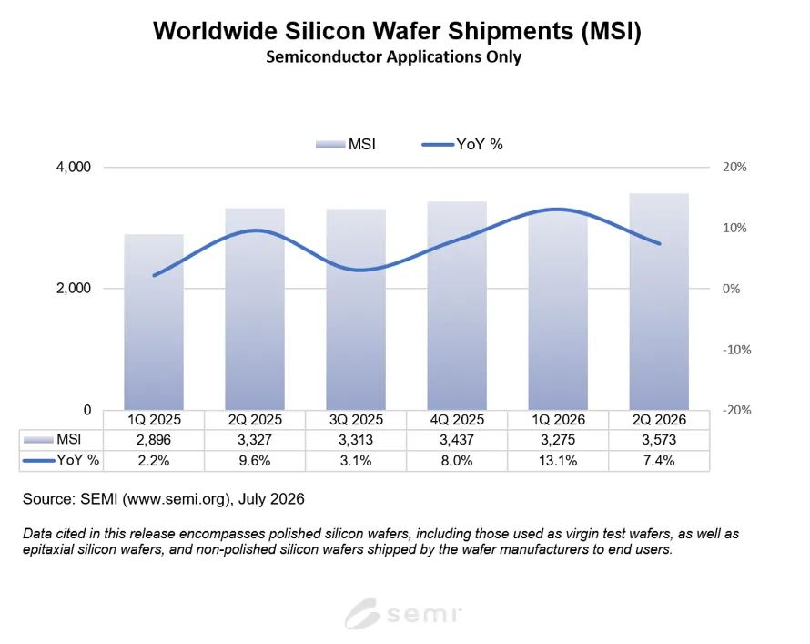
MILPITAS, Calif. — July 29, 2026 — The SEMI Silicon Manufacturers Group (SMG) reported today, in its quarterly analysis of the silicon wafer industry, that worldwide silicon wafer shipments increased 7.4% year-on-year to 3,573 million square inches (MSI) from the 3,327 MSI recorded during the same quarter of 2025. Shipments increased 9.1% quarter-over-quarter from the 3,275 MSI recorded during the first quarter of 2026. 

“Silicon wafer shipments maintained steady growth in the second quarter, driven by strong and increasing AI-related demand beyond advanced logic and memory to include power devices, photonics, and other markets,” said Ginji Yada, Chairman of SEMI SMG and Managing Executive Officer, General Manager, Sales and Marketing Division at SUMCO Corporation. “In addition, industrial and automotive demand is recovering, while memory price pressures are contributing to constrained PC and smartphone demand. Device manufacturers are investing heavily in capacity expansion, and silicon wafer demand growth is expected to continue.”

Silicon wafers are the fundamental building material for the majority of semiconductors, which are vital components of all electronic devices. The highly engineered thin disks are produced in diameters of up to 300 mm and serve as the substrate material on which most semiconductors are fabricated.

The SMG is a sub-committee of the SEMI Electronic Materials Group (EMG) and is open to SEMI members involved in manufacturing polycrystalline silicon, monocrystalline silicon or silicon wafers (e.g., as cut, polished, epitaxial). The SMG facilitates collective efforts on issues related to the silicon industry, including the development of statistics about the silicon industry.

For more information, visit SEMI Worldwide Silicon Wafer Shipment Statistics.

Follow SEMI Market Intelligence

Follow SEMI 

About SEMI

SEMI® is the global industry association connecting over 4,000 companies and 1.5 million professionals worldwide across the semiconductor and electronics design and manufacturing supply chain. We accelerate member collaboration on solutions to top industry challenges through Advocacy, Workforce Development, Sustainability, Supply Chain Management and other programs. Our SEMICON® expositions and events, technology communities, standards and market intelligence help advance our members’ business growth and innovations in design, devices, equipment, materials, services and software, enabling smarter, faster, more secure electronics. Visit www.semi.org, contact a regional office, and connect with SEMI on LinkedIn and X to learn more.


  • Advanced Manufacturing Investment Credit (AMIC) has become a critical asset in accelerating semiconductor growth in the U.S. to maintain competitiveness
  • Industry coalition warns that failure to act before the December 31, 2026, deadline threatens billions in planned U.S. semiconductor investment
  • SEMI also recommends Congress strengthen the credit by expanding it to include materials and design

WASHINGTON, D.C. — July 22, 2026 — SEMI, the global industry association serving the semiconductor and electronics design and manufacturing supply chain, today brought together executives from member companies for advocacy meetings on Capitol Hill focused on extending the tax credit for investments in building up the U.S. semiconductor ecosystem. As part of the SEMI Tax Day event, industry representatives are meeting with Members of Congress, including those serving on the House Ways and Means and Senate Finance Committees, to urge swift passage of a multi-year extension of the Section 48D Advanced Manufacturing Investment Credit (AMIC) before it lapses at the end of the year.

Enacted under the CHIPS and Science Act, the Section 48D credit provides a refundable 35% tax credit for qualified investment in semiconductor and semiconductor manufacturing equipment facilities. It has helped catalyze hundreds of billions of dollars in announced U.S. semiconductor investment across 28 states. Under current law, facilities must begin construction by December 31, 2026, to qualify — a deadline SEMI says is out of step with the ongoing need for semiconductor ecosystem expansion and the multi-year timelines required to site, permit, finance, and build a semiconductor facility.

“The Advanced Manufacturing Investment Credit has been one of the most effective tools this country has for winning semiconductor investment, and its looming expiration is creating real uncertainty for companies planning projects today,” said Joe Stockunas, President, SEMI Americas. “Congress has an opportunity to remove that uncertainty, maintain U.S technology competitiveness, and attract good-paying semiconductor industry jobs by preserving and strengthening the Section 48D tax credit. Our member companies came to Washington today to advocate for this crucial issue to extend and expand the tax credit before the end of the year.”

SEMI’s Request

SEMI's primary request of Congress is a multi-year extension of Section 48D ahead of the December 31, 2026, construction deadline, providing companies the certainty needed to plan, finance, and execute the next wave of U.S. semiconductor investment. SEMI also urged Congress to consider strengthening the credit by expanding eligibility to cover the full semiconductor supply chain, including materials, specialty chemicals and gases, and design activities that are currently excluded.

Why It Matters

Demand for semiconductors continues to accelerate, driven by artificial intelligence, quantum computing, defense, and biomedical applications. SEMI projects that 93 new fabs will come online globally by 2029 and that U.S. investment in front-end fabs and advanced packaging could grow from $24 billion in 2025 to as much as $81 billion annually by 2030 — growth that industry representatives say depends on maintaining a competitive, predictable federal tax incentive.

Major semiconductor producing economies are competing aggressively for that same investment. South Korea offers R&D tax incentives of 30-50% and 20-30% incentives for qualified investment costs across the semiconductor supply chain. Taiwan offers R&D credits of up to 35% for advanced node technologies along with import duty exemptions on specialized equipment. Japan provides a 20% corporate income tax reduction each fiscal year alongside targeted grants. Without comparable certainty in the U.S., industry representatives warned, new projects could increasingly be sited overseas.

“Semiconductor investment is happening on a global scale, and companies are making site-selection decisions right now that will play out over the next decade,” said Stockunas. “Allowing this credit to lapse doesn’t just slow down projects already underway — it risks sending the next wave of investment to countries that are working to attract it.”

Visit SEMI Global Advocacy to learn more about public policy efforts and developments.

About SEMI

SEMI® is the global industry association connecting over 4,000 companies and 1.5 million professionals worldwide across the semiconductor and electronics design and manufacturing supply chain. We accelerate member collaboration on solutions to top industry challenges through Advocacy, Workforce Development, Sustainability, Supply Chain Management and other programs. Our SEMICON® expositions and events, technology communities, standards and market intelligence help advance our members’ business growth and innovations in design, devices, equipment, materials, services and software, enabling smarter, faster, more secure electronics. Visit www.semi.org, contact a regional office, and connect with SEMI on LinkedIn and X to learn more.  


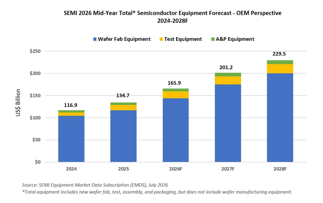
MILPITAS, Calif. — July 14, 2026 — Global sales of total semiconductor manufacturing equipment by original equipment manufacturers (OEMs) are forecast to reach a record high of $165.9 billion in 2026, increasing 23.2% year-on-year, SEMI announced today in its Mid-Year Total Semiconductor Equipment Forecast – OEM Perspective. Growth momentum is expected to continue through 2028, with total equipment sales forecast to reach a record $229.5 billion, marking five consecutive years of growth as AI-driven demand reshapes semiconductor manufacturing investment. 

The stronger outlook reflects accelerating investment in AI infrastructure, leading-edge logic, advanced memory, and back-end technologies needed to support higher compute density, high bandwidth memory (HBM)-related investment, and increasingly complex device architectures.

“AI is accelerating demand for more powerful and efficient chips, driving increased investment across the semiconductor capital equipment market,” said Ajit Manocha, SEMI president and CEO. “The mid-year forecast points to a higher equipment spending trajectory as chipmakers invest in the leading-edge logic, advanced memory, test and packaging capabilities required for the AI era.”
Semiconductor Equipment Sales by Segment 

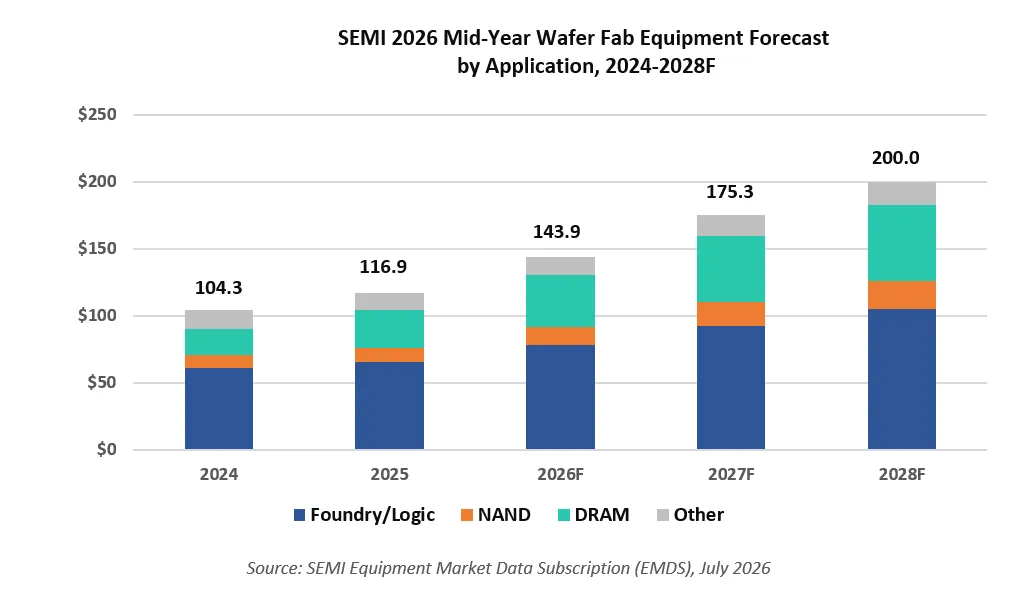
After registering a record $116.9 billion in sales last year, the Wafer Fab Equipment (WFE) segment, which includes wafer processing, mask/reticle, and fab facilities equipment, is projected to increase 23.1% to $143.9 billion in 2026. This represents a significant upward revision from SEMI’s 2025 year-end forecast and reflects stronger investment in advanced memory, especially HBM-related DRAM technologies, and leading-edge logic applications. WFE segment sales are projected to expand 21.8% in 2027 and 14.1% in 2028 to reach the $200 billion mark, as manufacturers accelerate capacity expansion and technology migration for AI-related workloads.

AI-related semiconductor demand is also driving expansion in back-end equipment. After surging 55.3% in 2025, semiconductor test equipment sales are projected to increase 31.0% to $15.3 billion in 2026, marking a strong upward revision from SEMI’s 2025 year-end forecast. Assembly and packaging equipment sales, which increased 20.8% in 2025, are projected to rise 9.6% to $6.7 billion in 2026, broadly in line with the prior forecast. Growth is expected to continue through 2028, with test equipment reaching $20.8 billion and assembly and packaging equipment reaching $8.6 billion, supported by increasing device complexity, advanced and heterogeneous packaging adoption, and more rigorous performance and reliability requirements for AI and HBM devices.

WFE Sales by Application

WFE sales for foundry and logic applications are expected to increase 18.9% year-over-year to $78.0 billion in 2026, driven by advanced-node capacity buildouts for AI accelerators, high-performance computing, and premium mobile processors. The segment is forecast to grow 18.1% in 2027 and 13.6% in 2028, reaching $104.7 billion, as the industry advances toward high-volume manufacturing at the 2nm gate-all-around node.

Memory-related equipment spending is projected to expand significantly through 2028, supported by HBM demand, advanced DRAM node migration, and NAND technology transitions. DRAM equipment sales are projected to rise 39.0% to $38.8 billion in 2026, followed by 27.4% growth in 2027 and 15.0% growth in 2028, reaching $56.9 billion. NAND equipment sales are expected to grow 30.7% to $13.9 billion in 2026, then increase 31.1% in 2027 and 14.5% in 2028, reaching $20.8 billion, driven by 3D NAND layer migration and investment in higher-density architectures.

Semiconductor Equipment Sales by Region

China, Taiwan and Korea are expected to remain the top three destinations for equipment spending through 2028. China is projected to maintain the leading position over the forecast period, though growth is expected to moderate in 2026 following elevated investment levels in recent years. In Taiwan, spending is supported by leading-edge capacity builds for AI and high-performance computing, while Korea’s equipment spending is driven by advanced memory technologies, including HBM. Other regions tracked are expected to see equipment spending increase in 2027 and 2028, supported by regionalization efforts, government incentives and targeted specialty capacity expansions.

The SEMI forecast is based on collective input from top equipment suppliers, the SEMI Worldwide Semiconductor Equipment Market Statistics (WWSEMS) data collection program, and the industry-recognized SEMI World Fab Forecast database. 

About SEMI Market Data

The Equipment Market Data Subscription (EMDS) from SEMI provides comprehensive market data for the global semiconductor equipment market. A subscription includes three reports: 

  • Monthly SEMI North American Billings Report, an early perspective of equipment market trends
  • Monthly Worldwide Semiconductor Equipment Market Statistics (WWSEMS), a detailed report of semiconductor equipment billings for seven regions and more than 22 market segments
  • Bi-annual Total Semiconductor Equipment Forecast – OEM Perspective, an outlook for the semiconductor equipment market

Download a sample EMDS report.

For more information about the report or to subscribe, please contact the SEMI Market Intelligence Team at [email protected]. More details are also available on the SEMI Market Data webpage.  

Follow SEMI Market Intelligence

Follow SEMI 

About SEMI

SEMI® is the global industry association connecting over 4,000 companies and 1.5 million professionals worldwide across the semiconductor and electronics design and manufacturing supply chain. We accelerate member collaboration on solutions to top industry challenges through Advocacy, Workforce Development, Sustainability, Supply Chain Management and other programs. Our SEMICON® expositions and events, technology communities, standards and market intelligence help advance our members’ business growth and innovations in design, devices, equipment, materials, services and software, enabling smarter, faster, more secure electronics. Visit www.semi.org, contact a regional office, and connect with SEMI on LinkedIn and X to learn more.

MILPITAS, Calif. - July 7, 2026 - SEMI and TechSearch International today announced the release of the 2026 edition of the Worldwide Assembly & Test Facility Database, a comprehensive resource tracking semiconductor back-end manufacturing facilities operated by integrated device manufacturers (IDMs) and outsourced semiconductor assembly and test (OSAT) companies worldwide.

The 2026 edition covers more than 820 facilities, up from 750 in the 2025 edition, and adds new fields that help users analyze not only where facilities are located and what assembly and test services they provide, but also the materials, platforms, technologies and end markets they support.

Based on the new classifications, more than 360 facilities report compound semiconductor capabilities, including sites supporting silicon carbide (SiC), gallium nitride (GaN), gallium arsenide (GaAs) and indium phosphide (InP). More than 170 facilities identify AI and high-performance computing (HPC) among their end-market focus, while more than 70 facilities support photonics and optical applications. The new fields also capture substrate and interposer platforms along with broader technology and module capabilities, providing clearer visibility into how global back-end infrastructure is aligning with emerging demand.

“AI infrastructure, photonics and compound semiconductors are expanding the range of capabilities required across semiconductor assembly and test,” said Clark Tseng, Senior Director of Market Intelligence at SEMI. “The 2026 database gives users a more detailed view of which facilities support these technologies and end markets, helping them assess supply-chain exposure, identify manufacturing partners and track the evolution of global back-end capabilities.”

The 2026 edition includes the following updates and enhancements:

  • Expanded Global Coverage: More than 820 facilities worldwide, an increase of more than 70 facilities from the 2025 edition. The largest additions to database coverage were in China and Taiwan.
  • Compound Semiconductor Visibility: New fields identify whether facilities support compound semiconductors and specify material types including SiC, GaN, GaAs and InP.
  • End-Market Focus: New classifications provide insight into facilities supporting AI/HPC, automotive, mobile and consumer, industrial, networking and telecom, photonics and optical, and other end markets.
  • Substrate and Interposer Platforms: New data identifies capabilities across laminate substrates, redistribution layers (RDL), ceramic substrates, silicon interposers and leadframes.
  • Technology and Module Capabilities: Expanded facility-level descriptions provide additional detail on advanced packaging, modules, test services and specialized technology capabilities.
  • Updated Facility Profiles: The database continues to provide current information on facility status, ownership, location, plant type, assembly and test capabilities, device focus, automotive certification and operating history.
  • Updated OSAT Market Benchmarks: The 2026 edition includes updated top 10 OSAT capital expenditure and top 20 OSAT revenue rankings.

The database supports semiconductor manufacturers, equipment and materials suppliers, packaging and test providers, investors, government agencies and analysts seeking to map global manufacturing footprints, compare facility-level capabilities, identify potential partners, evaluate regional concentration and monitor facility openings, closures, expansions and ownership changes.

To access the Worldwide Assembly & Test Facility Database, visit https://www.semi.org/en/products-services/market-data/ww-assembly-test-facility-database. For more information on the report or to subscribe, please contact the SEMI Market Intelligence Team at [email protected]. More details are also available on the SEMI Market Data webpage.  

Follow SEMI Market Intelligence

Follow SEMI 

About SEMI

SEMI® is the global industry association connecting over 4,000 companies and 1.5 million professionals worldwide across the semiconductor and electronics design and manufacturing supply chain. We accelerate member collaboration on solutions to top industry challenges through Advocacy, Workforce Development, Sustainability, Supply Chain Management and other programs. Our SEMICON® expositions and events, technology communities, standards and market intelligence help advance our members’ business growth and innovations in design, devices, equipment, materials, services and software, enabling smarter, faster, more secure electronics. Visit www.semi.org, contact a regional office, and connect with SEMI on LinkedIn and X to learn more.  

About TechSearch International

TechSearch International, Inc., founded in 1987, is a market research leader specializing in technology trends in microelectronics packaging and assembly. Multi- and single-client services encompass technology licensing, strategic planning, and market and technology analysis. TechSearch International professionals have an extensive network of ~20,000 contacts in North America, Asia, and Europe. For more information, contact TechSearch International at [email protected] or tel: 512-372-8887 or see www.techsearchinc.com. Follow us on LinkedIn.