downloadGroupGroupnoun_press release_995423_000000 copyGroupnoun_Feed_96767_000000Group 19noun_pictures_1817522_000000Member company iconResource item iconStore item iconGroup 19Group 19noun_Photo_2085192_000000 Copynoun_presentation_2096081_000000Group 19Group Copy 7noun_webinar_692730_000000Path
Skip to main content
Default Banner Image

SEMI Press Release

ID
semi-press-release

MILPITAS, Calif. — May 27, 2026 — SEMI, the industry association serving the global semiconductor and electronics design and manufacturing supply chain, today announced the availability of a new industry research report focused on the glass core substrate market and trends, produced in collaboration with Global Net Corp. (GNC). The Glass Core Substrate Market and Development Trends Report examines the emerging market for glass core substrates, a potential next-generation packaging technology attracting increased attention as AI and high-performance computing (HPC) drive demand for larger and more advanced semiconductor packages.

“As chipmakers look for new ways to improve system performance beyond traditional device scaling, advanced packaging has become a critical area of innovation,” said Clark Tseng, Senior Director of Market Intelligence, SEMI. “Glass core substrates are being evaluated as one possible solution for future high-end packages because they may help support larger package sizes, finer interconnects, and improved dimensional stability compared to conventional package-substrate materials. This new report helps industry stakeholders understand where glass core substrates may fit in the next phase of packaging technology and what challenges must be addressed to achieve broader adoption.”

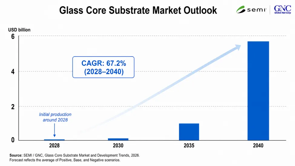
The report highlights increasing industry activity and investment around glass core substrates as companies prepare for the next phase of advanced packaging—providing an independent view of the technology’s market potential, development status, key players, and remaining barriers to commercialization. Under the report’s market-development scenarios, initial production could begin around 2028 in selected high-performance applications, with adoption expanding over time across larger and more complex package architectures. Based on the average of its Positive, Base, and Negative scenarios, the report projects a compound annual growth rate (CAGR) of 67.2% from 2028 to 2040. It also maps an increasingly active global development ecosystem, with companies and research organizations across Asia, North America and Europe advancing glass core substrate technologies.
 

Key topics covered in the report include:

  • Market outlook and adoption scenarios for glass core substrates 
  • Technology drivers and barriers to commercialization 
  • Expected applications in AI, HPC, advanced processors, co-packaged optics, and image sensors 
  • Company activities across substrates, glass materials, equipment, processing, inspection, and related supply-chain segments 
  • Development hubs, consortia, and supply-chain structure 
  • Forecast scenarios through 2040 

The Glass Core Substrate Market and Development Trends report is available in English and Japanese editions through SEMI Market Intelligence. Download the report.

For more information, please visit the Glass Core Substrate Market and Development Trends page or contact the SEMI Market Intelligence Team at [email protected].

Follow SEMI Market Intelligence

Follow SEMI 

About Global Net Corp.

Global Net Corp. is a Tokyo-based company serving the semiconductor and electronics industries. Established in 1990, the company provides wafer processing, equipment sales, consulting, technical seminars, research groups, and industry publishing services. Its technical and market coverage spans semiconductors, electronics, FPD, packaging, CMP, and related manufacturing processes.

About SEMI

SEMI® is the global industry association connecting over 4,000 companies and 1.5 million professionals worldwide across the semiconductor and electronics design and manufacturing supply chain. We accelerate member collaboration on solutions to top industry challenges through Advocacy, Workforce Development, Sustainability, Supply Chain Management and other programs. Our SEMICON® expositions and events, technology coalitions, standards and market intelligence help advance our members’ business growth and innovations in design, devices, equipment, materials, services and software, enabling smarter, faster, more secure electronics. Visit www.semi.org, contact a regional office, and connect with SEMI on LinkedIn and X to learn more.

MILPITAS, Calif. – May 19, 2026 – FlexTech, a SEMI Technology Coalition, today issued a request for proposals (RFP) to advance flexible hybrid electronics (FHE) technologies, including the development of advanced materials and additive processing. Selected projects will receive cash awards ranging from $250,000 to $500,000. The program is funded by the Army Research Laboratory (ARL). ARL funding will be matched with contributions by selected recipients to cover total project cost.

The RFP seeks proposals targeting FHE advances in the following areas:

  • Flexible, Moldable Electronics
  • Advanced Bonding Reliability
  • Novel Flexible Energy Storage Beyond Conventional Architectures
  • 2D Materials

Organizations submitting proposals will be evaluated based on their capabilities, experiences, and strengths. See the FlexTech 2026 RFP for more details on the evaluation process.

Proposal Submissions

Full proposal submissions are due July 6, 2026. Awardees will be notified following the review of proposals by the RFP committee. The committee consists of FlexTech Council members and other subject matter experts (SMEs). Evaluation criteria include:

  • Rationale
  • Budget
  • Collaboration value
  • Dual-use (industry and military) applicability
  • Relevance to the topics and the FHE ecosystem 
  • Schedules and milestones
  • Reasonable and stretch deliverables
  • Overall proposal quality 

Informational Webinar on May 20, 2026

To help organizations craft their proposals, FlexTech staff will review the RFP topics and the submission and review process during a live webinar on May 20, 2026 at 10:00 a.m. PDT. A recording will be available for registrants unable to attend the event. Register for the webinar. 

About FlexTech RFPs

FlexTech RFPs support technical approaches that are revolutionary or have a significant element of risk, as well as approaches that are evolutionary improvements upon existing capability, which tend to be less risky and involve shorter development and delivery intervals.

FlexTech encourages partnerships among industrial companies, R&D organizations, and university teams. Development partners retain ownership of intellectual property developed under FlexTech agreements. If you have any questions, please contact [email protected].

About FlexTech

FlexTech is an industry-led public/private partnership that brings together scientists, engineers, and business development professionals from industry, government, and universities to collaboratively initiate research and the development of the infrastructure required to develop world-class FHE devices and products. Learn more. 

About SEMI

SEMI® is the global industry association connecting over 4,000 companies and 1.5 million professionals worldwide across the semiconductor and electronics design and manufacturing supply chain. We accelerate member collaboration on solutions to top industry challenges through Advocacy, Workforce Development, Sustainability, Supply Chain Management and other programs. Our SEMICON® expositions and events, technology coalitions, standards and market intelligence help advance our members’ business growth and innovations in design, devices, equipment, materials, services and software, enabling smarter, faster, more secure electronics. Visit www.semi.org, contact a regional office, and connect with SEMI on LinkedIn and X to learn more.  

WASHINGTON, D.C. – May 14, 2026 — SEMI, the industry association serving the global semiconductor and electronics design and manufacturing supply chain, and 23 member companies on the SEMI Tax Policy Committee, issued a letter to the U.S. Congress urging immediate passage of a multi-year extension of the Advanced Manufacturing Investment Credit (AMIC). The letter’s signatories span the end-to-end semiconductor supply chain and underscore how AMIC drives the major investments essential to meet surging market demand.

“The Advanced Manufacturing Investment Credit is essential to accelerating semiconductor growth in the United States—especially as semiconductor demand from emerging technologies like artificial intelligence and quantum technologies continues to surge,” said Joe Stockunas, SEMI Americas President. “The AMIC’s looming expiration threatens business planning and long-term capital investment. Congress must act now to ensure American competitiveness and a resilient supply chain.”  
The U.S. semiconductor industry is scaling rapidly to power emerging technologies, telecommunications, and bioengineering—but that growth requires billions in sustained upfront investment. The AMIC’s 35% investment tax credit helps mitigate those costs. Without extension, the credit’s expiration creates a planning cliff that could derail the industry’s historic momentum exactly when companies are committing to next-generation projects. A multi-year extension of the AMIC would sustain U.S. investment, strengthen domestic manufacturing, and cement U.S. global technological leadership.

The letter also highlights to Congress the value of expanding eligibility for the credit across the full semiconductor supply chain. Today semiconductor materials, chemicals, and electronic design automation (EDA) tools are excluded from the AMIC, risking domestic investment efforts and ceding ground to global competitors.

SEMI and its members urge Congress to extend the AMIC beyond the 2026 expiration date and stand ready to partner with Congress to make that a reality.

The letter was signed by SEMI Tax Policy Committee members:

  • Advantest America Inc.
  • Analog Devices
  • Applied Materials, Inc.
  • ASM
  • ASML
  • Axcelis Technologies Inc.
  • CoorsTek
  • Entegris, Inc.
  • GlobalWafers America, LLC
  • GlobalFoundries
  • Intel Corporation
  • KLA Corporation
  • Lam Research Corporation
  • onsemi
  • Qnity Electronics, Inc. 
  • Roos Instruments
  • Samsung
  • SK hynix Inc.
  • SkyWater Technology
  • Teradyne, Inc. 
  • Texas Instruments 
  • Tokyo Electron U.S. Holdings, Inc.
  • TSMC

View SEMI’s 2026 U.S. Policy Strategy to learn more about SEMI’s top policy priorities. For updates on SEMI’s public policy efforts and developments, visit SEMI Global Advocacy.

About SEMI

SEMI® is the global industry association connecting over 4,000 companies and 1.5 million professionals worldwide across the semiconductor and electronics design and manufacturing supply chain. We accelerate member collaboration on solutions to top industry challenges through Advocacy, Workforce Development, Sustainability, Supply Chain Management and other programs. Our SEMICON® expositions and events, technology communities, standards and market intelligence help advance our members’ business growth and innovations in design, devices, equipment, materials, services and software, enabling smarter, faster, more secure electronics. Visit www.semi.org, contact a regional office, and connect with SEMI on LinkedIn and X to learn more.

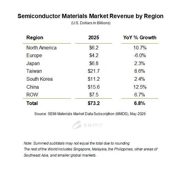
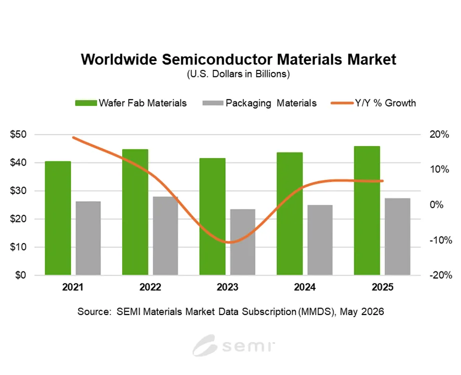
MILPITAS, Calif. — May 12, 2026 — Global semiconductor materials market revenue increased 6.8% year-over-year to $73.2 billion in 2025, SEMI, reported today in its Materials Market Data Subscription (MMDS). Growth was supported by gains in both the wafer fab materials and packaging materials segments, reflecting higher process complexity, advanced-node demand, and continued investment in high-performance computing and high-bandwidth memory manufacturing. 

Wafer fabrication materials revenue increased 5.4% to $45.8 billion. Lithography-related materials, including photomask, photoresist and ancillaries, along with wet chemicals, posted strong double-digit growth as higher process intensity and tighter lithography requirements continued to increase materials consumption.

Packaging materials revenue grew 9.3% to $27.4 billion in 2025. Substrates and bonding wire led the increase, supported by higher gold prices in bonding wire and stronger demand for advanced substrates.

Taiwan remained the largest consumer of semiconductor materials for the 16th consecutive year, with revenue of $21.7 billion in 2025. China ranked second at $15.6 billion, supported by double-digit growth, followed by South Korea at $11.2 billion. All regions except Europe posted year-over-year increases, with China and North America recording the strongest growth among major regions.

The Materials Market Data Subscription (MMDS) from SEMI provides annual revenue with 10 years of historical data and a two-year forecast. The annual subscription includes quarterly updates for the materials segment and reports revenue for seven market regions (North America, Europe, Japan, Taiwan, South Korea, China and Rest of World). The report also features detailed historical data for silicon shipments and revenues for photoresist, photoresist ancillaries, process gases and lead frames.

For more information about the report or to subscribe, please contact the SEMI Market Intelligence Team at [email protected]. More details are also available on the SEMI Market Data webpage.  

Download a sample of the MMDS report. 

Follow SEMI Market Intelligence

Follow SEMI 

About SEMI

SEMI® is the global industry association connecting over 4,000 companies and 1.5 million professionals worldwide across the semiconductor and electronics design and manufacturing supply chain. We accelerate member collaboration on solutions to top industry challenges through Advocacy, Workforce Development, Sustainability, Supply Chain Management and other programs. Our SEMICON® expositions and events, technology communities, standards and market intelligence help advance our members’ business growth and innovations in design, devices, equipment, materials, services and software, enabling smarter, faster, more secure electronics. Visit www.semi.org, contact a regional office, and connect with SEMI on LinkedIn and X to learn more.

DRESDEN, Germany — May 6, 2026 — Global experts in advanced semiconductor packaging and 3D integration will convene at the annual SEMI 3D & Systems Summit, June 17–19, 2026, in Dresden, Germany. The Summit will deliver cutting-edge insights into the technologies and strategies shaping the future of heterogeneous systems and Europe's semiconductor ecosystem. Registration is open.

Themed Enabling Next-Gen Heterogeneous Systems Integration, this year's Summit will feature a program spanning geopolitical dynamics, market trends, AI hardware architectures, chiplet design, AR/VR and wearable intelligence, and the latest advancements in hybrid bonding and co-packaged optics.

“We look forward to welcoming industry leaders, innovators, and researchers to the 3D & Systems Summit 2026 in Dresden," said Laith Altimime, President of SEMI Europe. “As heterogeneous integration, chiplet architectures, and advanced packaging redefine system performance, the Summit provides a critical platform to align technology roadmaps, accelerate innovation, and strengthen Europe's position in next-generation semiconductor systems.”

3D & Systems Summit Sessions

Session 1: Market Trends and Europe's Technological Positioning

Executive leaders will examine the shifting geopolitical dynamics reshaping semiconductor supply chains, exploring industrial policy, regional fab strategies, and global benchmarking. Speakers will assess where Europe stands today and what is required to secure technology sovereignty across critical domains.

Session 2: Advanced Packaging Capacity: From Lab Innovation to Fab Deployment

Industry experts will address the full spectrum of advanced packaging, from fan-out technologies and outsourced semiconductor assembly and test (OSAT) strategies to supply chain considerations and lab-to-fab technology transfer. The session will highlight European strengths and the steps needed to scale advanced packaging capacity regionally.

Session 3: Hybrid Bonding: Die-to-Wafer & Wafer-to-Wafer

Specialists will examine hybrid bonding as a cornerstone of high-density 3D integration, covering die-to-wafer and wafer-to-wafer techniques, DRAM stacking, reliability engineering, and integration challenges across memory, logic, and advanced packaging.

Session 4: Photonics at Scale: Co-Packaged Optics

Industry leaders will explore co-packaged optics and photonic integration as key enablers of high-bandwidth communication, AI acceleration, and energy-efficient data movement, with discussions spanning optical interconnects, quantum photonics, and high-volume manufacturing readiness.

Session 5: Design Leadership: Chiplets & System Architecture

Experts will highlight chiplet architectures, CPU startups, and 3D integration strategy, showcasing the cutting-edge design activities that are positioning Europe as an emerging leader in system-level semiconductor architectures.

Session 6: AR/VR & Wearable Intelligence

Speakers will explore the convergence of optics, photonics, packaging, and efficient computing driving the next generation of AR/VR and spatial computing platforms, from displays and imagers to optical engines and low-power compute for consumer and industrial applications.

Global Leaders to Present

3D & Systems Summit presenters include experts from these global leaders

  • Adeia
  • ALLOS Semiconductors 
  • ams-OSRAM
  • ASML 
  • CEA-Leti
  • Confovis
  • Evatec
  • GlobalFoundries
  • imec
  • KLA 
  • Lam Research 
  • Murata
  • NXP Semiconductors 
  • STMicroelectronics
  • TechSearch International
  • Yole Group

Exhibition and Business Networking

The 3D & Systems Summit will feature an exclusive exhibition area showcasing industry leaders alongside innovative emerging companies, as well as business-to-business matchmaking and networking opportunities throughout the event.

The networking reception will take place at the Hilton Dresden Hotel on the first evening prior to the Summit. The networking dinner will be held aboard a historic paddle steamer on the Elbe River, following the final sessions of the first day.

Networking dinner registration is reserved exclusively for 3D & Systems Summit 2026 participants.

3D & Systems Summit Sponsors

Platinum: Adeia, ASE, Comet, Confovis, Lam Research

Gold: Evatec

Event: ASMPT, EV Group, imec, MKS Atotech

For more details, please visit the 3D & Systems Summit 2026 website and connect with SEMI Europe on LinkedIn or YouTube @SEMIEurope (#3DSummit).

Call for Abstracts Open for the 2026 Advanced Packaging Conference (APC) 

SEMI Europe has opened the call for abstracts for the 2026 Advanced Packaging Conference (APC), inviting industry leaders, researchers, and innovators to submit presentations highlighting the latest breakthroughs in advanced packaging, testing, and heterogeneous integration technologies. 

Themed Power and Interconnects Innovations Enabling AI System Performance, APC 2026 will explore how innovations such as 2.5D/3D integration, chiplet architectures, co-packaged optics, advanced materials, AI-driven design flows, and next-generation thermal and power management are enabling the future of AI, high-performance computing (HPC), automotive, and edge applications. Abstract submissions are open through July 1, 2026.

About SEMI 

SEMI® is the global industry association connecting over 4,000 companies and 1.5 million professionals worldwide across the semiconductor and electronics design and manufacturing supply chain. We accelerate member collaboration on solutions to top industry challenges through Advocacy, Workforce Development, Sustainability, Supply Chain Management and other programs. Our SEMICON® expositions and events, technology communities, standards and market intelligence help advance our members’ business growth and innovations in design, devices, equipment, materials, services and software, enabling smarter, faster, more secure electronics. Visit www.semi.org, contact a regional office, and connect with SEMI on LinkedIn and X to learn more.  

BRUSSELS – April 27, 2026 – SEMI Europe today announced the publication of its Position Paper on the Chips Act 2.0, presenting a set of strategic recommendations aimed at reinforcing and future-proofing Europe’s semiconductor policy framework. While the first European Chips Act represented a significant milestone for the region’s semiconductor ecosystem, SEMI Europe now calls on policymakers to address the structural challenges that could constrain its long-term impact.

“Research and product development, chip design, equipment, materials, fabrication and advanced packaging are all interconnected elements of a single ecosystem—one in which success relies on every component functioning in harmony,” said Laith Altimime, President of SEMI Europe.

Building on this perspective, SEMI Europe emphasizes that the effectiveness of the Chips Act 2.0 will depend on its capacity to strengthen capabilities across the entire semiconductor value chain—from design and materials to equipment, as well as front-end and back-end manufacturing. Achieving this will require a revision of the “First-of-a-Kind” definition and an expansion of the Pillar II framework to better reflect the full breadth of the industry.

The position paper also highlights the need to translate Europe’s strong research base into tangible industrial outcomes. To address this structural gap, SEMI Europe advocates for increased industry participation in EU-funded R&D programmes, the creation of dedicated industrialisation initiatives, and the development of tailored instruments to support smaller, innovative players.

Finally, to position the Chips Act 2.0 as a truly strategic instrument, closer alignment with other legislative frameworks will be essential, ensuring its integration into a broader EU technology strategy. Complementary measures—such as targeted tax incentives, reliable access to water and energy resources, and the establishment of a dedicated governing body—will be critical in enhancing Europe’s attractiveness as a destination for semiconductor investment.

SEMI Europe Advocacy 

Discover how SEMI Europe Advocacy & Public Policy supports the microelectronics industry across sustainability, trade, talent, and R&D—or become involved by contacting [email protected].  

About SEMI 

SEMI® is the global industry association connecting over 4,000 companies and 1.5 million professionals worldwide across the semiconductor and electronics design and manufacturing supply chain. We accelerate member collaboration on solutions to top industry challenges through Advocacy, Workforce Development, Sustainability, Supply Chain Management, and other programs. Our SEMICON® expositions and events, technology communities, standards, and market intelligence help advance our members’ business growth and innovations in design, devices, equipment, materials, services, and software, enabling smarter, faster, more secure electronics. Visit www.semi.org, contact a regional office, and connect with SEMI on LinkedIn and X to learn more. 

MILPITAS, Calif. — April 30, 2026 — SEMI, the industry association serving the global semiconductor and electronics design and manufacturing supply chain, today announced the appointment of Julie Rogers as Executive Director of the Electronic System Design Alliance (ESDA), a SEMI Technology Community.

In her new position, Rogers will lead global programs supporting the electronic design automation (EDA) and semiconductor ecosystem. She will oversee strategy, member initiatives, and high-impact events that connect EDA leaders, semiconductor companies, and system designers. Rogers replaces Robert P. Smith who has moved into an advisory role after serving as Executive Director for 11 years. 

“Julie’s leadership, industry insight, and collaborative approach will bring fresh energy and new ideas to strengthen the ESD Alliance and deliver even greater value to our global members,” said Ajit Manocha, President and CEO, SEMI. “Her longstanding tenure with SEMI and the ESDA has given her a deep understanding of our members’ needs and the evolving semiconductor industry landscape. We extend our gratitude to Bob Smith for his leadership as Executive Director over the past 11 years and look forward to his continued support as an ESDA advisor.”

Rogers brings more than 30 years of experience driving growth, visibility, and alignment across complex, highly technical markets. She is widely recognized for her leadership in driving industry collaboration, technical conferences, executive engagement, and ecosystem development. Over the past decade, she served as Director of Marketing and Operations for ESDA, congruent with over seven years as Director of Marketing for SEMI Americas, where she led integrated marketing campaigns, digital strategy, member development, brand advancement, media trades, and public relations efforts. 

Earlier in her career, Rogers founded and led a successful marketing firm specializing in large‑scale event planning and grant writing for healthcare technology and medical device companies. She also brings a strong background in broadcast media, further strengthening her ability to amplify thought leadership and industry impact. Rogers holds a Bachelor of Arts in Marketing from California State University, Sacramento.

About the Electronic System Design Alliance

The Electronic System Design (ESD) Alliance, a SEMI Technology Community, is the central voice to communicate and promote the value of the semiconductor design ecosystem as a vital component of the global electronics industry. As an international association of companies providing goods and services throughout the semiconductor design ecosystem, it is a forum to address technical, marketing, economic and legislative issues affecting the entire industry. For more information about the ESD Alliance, visit http://esd-alliance.org.

Follow the ESD Alliance

About SEMI

SEMI® is the global industry association connecting over 4,000 companies and 1.5 million professionals worldwide across the semiconductor and electronics design and manufacturing supply chain. We accelerate member collaboration on solutions to top industry challenges through Advocacy, Workforce Development, Sustainability, Supply Chain Management and other programs. Our SEMICON® expositions and events, technology communities, standards and market intelligence help advance our members’ business growth and innovations in design, devices, equipment, materials, services and software, enabling smarter, faster, more secure electronics. Visit www.semi.org, contact a regional office, and connect with SEMI on LinkedIn and X to learn more.

MILPITAS, Calif — April 30, 2026 —The Electronic System Design Alliance (ESD Alliance), a SEMI Technology Community, today announced its annual Executive Outlook event for semiconductor EDA, agentic AI and IP company executives. This year’s panel will be held on Wednesday, June 10, at Cadence Design Systems’ headquarters in San Jose, Calif. beginning at 5:30 p.m. with networking and dinner, followed by a panel discussion at 6:30 p.m. Registration is open.

The theme “How Will Agentic AI Change Chip Design and Verification?” will guide featured EDA and emerging agentic AI company executives and entrepreneurs as they discuss changes within chip design and verification as agentic AI tools become more mainstream. Moderated by Ed Sperling, Semiconductor Engineering’s Editor in Chief, panelists will distill the excitement surrounding the innovation in chip design and verification, collaboration between traditional EDA and agentic AI startups and broader implications for technological advancements. 
Panelists:

  • Dave Kelf, CEO of Breker Verification Systems
  • Cindy Cui, VP of Global Customer Success at ChipAgents 
  • Shelly Henry, CEO of Moores LabAI
  • Ann Wu, CEO at Silimate
  • Vince Wong, Head of AI Development at Verific Design Automation

Location:

Cadence Design Systems
2655 Seely Avenue
San Jose, CA 95134

Tickets for the event are free for SEMI/ESDA members and $40 per person for non-members. For more information, visit the event page.

About the Electronic System Design Alliance

The Electronic System Design (ESD) Alliance, a SEMI Technology Community, is the central voice to communicate and promote the value of the semiconductor design ecosystem as a vital component of the global electronics industry. As an international association of companies providing goods and services throughout the semiconductor design ecosystem, it is a forum to address technical, marketing, economic and legislative issues affecting the entire industry. For more information about the ESD Alliance, visit http://esd-alliance.org.

Follow the ESD Alliance

About SEMI

SEMI® is the global industry association connecting over 4,000 companies and 1.5 million professionals worldwide across the semiconductor and electronics design and manufacturing supply chain. We accelerate member collaboration on solutions to top industry challenges through Advocacy, Workforce Development, Sustainability, Supply Chain Management and other programs. Our SEMICON® expositions and events, technology communities, standards and market intelligence help advance our members’ business growth and innovations in design, devices, equipment, materials, services and software, enabling smarter, faster, more secure electronics. Visit www.semi.org, contact a regional office, and connect with SEMI on LinkedIn and X to learn more.

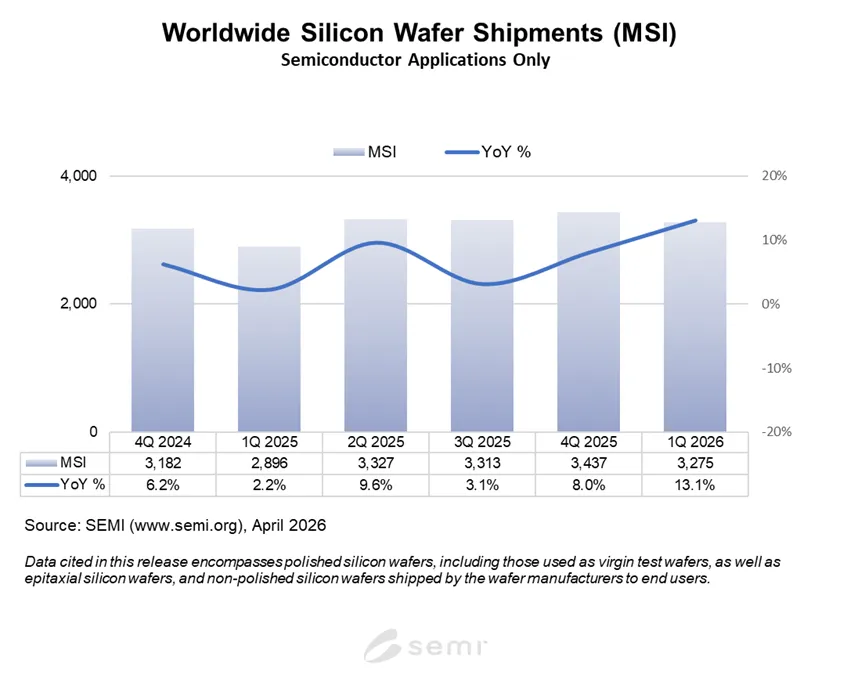
MILPITAS, Calif. — April 29, 2026 — The SEMI Silicon Manufacturers Group (SMG) reported today, in its quarterly analysis of the silicon wafer industry, that worldwide silicon wafer shipments increased 13.1% year-on-year to 3,275 million square inches (MSI) from the 2,896 MSI recorded during the same quarter of 2025. Sequentially, shipments declined 4.7% quarter-over-quarter from the 3,437 MSI recorded during the fourth quarter of 2025 in line with typical seasonality. 

“Silicon wafer demand related to AI data centers continues to be strong, including advanced logic and memory, and also now extending to power management devices,” said Ginji Yada, Chairman of SEMI SMG and Managing Executive Officer, General Manager, Sales and Marketing Division at SUMCO Corporation. “Overall, silicon wafer demand has improved, but the recovery is not uniform. Many device companies have noted improvements in the industrial semiconductor segment, and this is creating a more broad-based recovery as wafer inventory is absorbed. Weaker smartphone and PC shipments in the first quarter of this year may show the impact of tighter supply of memory due to AI high bandwidth memory (HBM) allocation decisions.”

Silicon wafers are the fundamental building material for the majority of semiconductors, which are vital components of all electronic devices. The highly engineered thin disks are produced in diameters of up to 300 mm and serve as the substrate material on which most semiconductors are fabricated.

The SMG is a sub-committee of the SEMI Electronic Materials Group (EMG) and is open to SEMI members involved in manufacturing polycrystalline silicon, monocrystalline silicon or silicon wafers (e.g., as cut, polished, epitaxial). The SMG facilitates collective efforts on issues related to the silicon industry, including the development of statistics about the silicon industry.

For more information, visit SEMI Worldwide Silicon Wafer Shipment Statistics.

Follow SEMI Market Intelligence

Follow SEMI 

About SEMI

SEMI® is the global industry association connecting over 4,000 companies and 1.5 million professionals worldwide across the semiconductor and electronics design and manufacturing supply chain. We accelerate member collaboration on solutions to top industry challenges through Advocacy, Workforce Development, Sustainability, Supply Chain Management and other programs. Our SEMICON® expositions and events, technology communities, standards and market intelligence help advance our members’ business growth and innovations in design, devices, equipment, materials, services and software, enabling smarter, faster, more secure electronics. Visit www.semi.org, contact a regional office, and connect with SEMI on LinkedIn and X to learn more.
 

MILPITAS, Calif. — April 22, 2026 — SEMI, the industry association serving the global semiconductor and electronics design and manufacturing supply chain, today announced the program for its 37th annual Advanced Semiconductor Manufacturing Conference (ASMC), taking place from May 11-14 in Albany, New York. The premier, four-day technical conference will feature more than 100 speakers, convening semiconductor industry leaders to solve core manufacturing challenges in areas including advanced materials, big data management, process control, wafer-level processing, and yield optimization. Registration is open.

ASMC 2026 Keynotes 

Challenges and Opportunities for Semiconductor Manufacturing Equipment in the AI Age

  • Presented by Gert Leusink, Vice President, Technology at Tokyo Electron Limited 
  • Tuesday, May 12

The Use of AI in High Volume Manufacturing: From Concept to Application

  • Presented by Sujieth Vaasan, Vice President, Digital Manufacturing at GlobalFoundries
  • Wednesday, May 13

Panel Discussion on Quantum Computing and Manufacturing Challenges

  • Panelists include Christy Tyberg, IBM Quantum; Tim Rogers, IonQ; Raja Katta, Rigetti Computing; Gordon Harling, CMC Microsystems; and Vimal Kamineni, PsiQuantum, and moderated by Ekta Bhatia, NY Creates
  • Wednesday, May 13

Industry Market Forecast

  • Presented by Robert Maire, President at Semiconductor Advisors
  • Thursday, May 14

Tutorial Presentation - From Hype to Implementation: Building the Core Pillars for AI in Semiconductors

Despite intense executive interest and extensive pilot activity, more than 70% of semiconductor AI initiatives stall before achieving enterprise-scale adoption. On Tuesday, May 12, Jonathan Holt, Senior Director of Product Management at PDF Solutions, will offer an actionable blueprint for high-value AI implementation to help bridge this gap. 

Partner Programs in Conjunction with ASMC 2026

SEMI University Workshops: Returning for the second time at ASMC, SEMI U will offer three in-person, instructor-led trainings: Understanding Semiconductor Technology & Business, Advanced IC Packaging & Assembly, and Overview of Semiconductor Manufacturing. ASMC attendees receive a $100 discount on SEMI U registration.

Women in Semiconductors (WiS): Open to all industry professionals, the WiS program will focus on strategies for building influence, leading with confidence, and expanding career opportunities. ASMC registrants receive complimentary registration. 

SEMI Standards Spring Meetings: The SEMI Standards process has been used to create more than 1,000 industry-approved standards and guidelines, based on the work of more than 6,000 volunteers. All SEMI Standards members are welcome to participate in the 2026 Spring Meetings. Register for membership at no cost.

SCIS General Meeting: The Semiconductor Components, Instruments, and Subsystems (SCIS) Technology Community General Meeting will take place on Thursday, May 14. All SEMI SCIS members are welcome to attend.                    

Glass4Chips Summit: Hosted at NY Creates on May 14 and at the Hilton Albany on May 15, this two-day summit will address barriers to glass substrate adoption and outline strategies to strengthen the U.S. glass supply chain. This will be held in partnership with SEMI, NY Creates, and FuzeHub. Registration is open.

ASMC 2026 is co‑chaired by Olaf Storbeck, Lead Principal Thermal Processes at Infineon Technologies, and Thirumalesh Bannuru, former Area Manager at Wolfspeed. 

For full conference details, please visit the ASMC website or contact Taylor Zhao at [email protected].

About SEMI

SEMI® is the global industry association connecting over 3,000 member companies and 1.5 million professionals worldwide across the semiconductor and electronics design and manufacturing supply chain. We accelerate member collaboration on solutions to top industry challenges through Advocacy, Workforce Development, Sustainability, Supply Chain Management and other programs. Our SEMICON® expositions and events, technology communities, standards and market intelligence help advance our members’ business growth and innovations in design, devices, equipment, materials, services and software, enabling smarter, faster, more secure electronics. Visit www.semi.org, contact a regional office, and connect with SEMI on LinkedIn and X to learn more.