downloadGroupGroupnoun_press release_995423_000000 copyGroupnoun_Feed_96767_000000Group 19noun_pictures_1817522_000000Member company iconResource item iconStore item iconGroup 19Group 19noun_Photo_2085192_000000 Copynoun_presentation_2096081_000000Group 19Group Copy 7noun_webinar_692730_000000Path
Skip to main content
Default Banner Image

SEMI Press Release

ID
semi-press-release

SAN FRANCISCO – Oct. 13, 2026 – SEMI, the industry association advancing the global semiconductor and electronics design and manufacturing supply chain, today announced Kulicke & Soffa as the recipient of the 2026 SEMI Award for North America. The company was selected for its formic acid in situ bonding technology, a fluxless thermocompression bonding (TCB) approach that’s central to the progression of heterogeneous integration. SEMI Americas presented the award to Kulicke & Soffa during the CEO Summit Keynotes at SEMICON West. 

Conventional TCB and hybrid bonding both present scaling challenges. At 50-micron pitches and below, post-bond liquid flux cleaning becomes extremely difficult and time-consuming. Conversely, while hybrid bonding is state-of-the-art, its high cost and manufacturing complexity limit accessibility. Kulicke & Soffa overcame these hurdles by combining in situ formic acid oxide reduction with plasma pre-cleaning across its high-volume TCB platforms, delivering hybrid bonding-level performance at a significantly lower cost. 

“As heterogeneous integration evolves, overcoming interconnect limitations becomes increasingly important for maintaining our industry’s ambitious growth trajectory,” said Joe Stockunas, president, SEMI Americas. “We’re honored to recognize Kulicke & Soffa for its outstanding breakthrough in fluxless TCB, a vital technology that’s helping the industry meet the rising demands of AI and high-performance computing. Kulicke & Soffa is a founding member of SEMI and is celebrating their 75th anniversary this year, demonstrating our industry’s ongoing drive to innovate.”

Built into solutions like APTURA™, Kulicke & Soffa’s pioneering technology offers multiple oxide removal strategies in a single platform. This results in the ability to achieve ultra-fine interconnect pitches below 10 microns, thereby meeting interconnect density requirements for heterogeneous integration and silicon photonics. The APTURA machine is designed to work flexibly across wafers, substrates, and 310 mm panels. 

“As features continue to shrink, our fluxless TCB technology is helping build the solid foundation required for advancing the industry’s Heterogeneous Integration Roadmap,” said Raj Talluri, President and Chief Executive Officer, Kulicke & Soffa. “We are proud to receive this recognition from SEMI Americas, which reflects the dedication and innovative spirit of our entire team around the world.”

Established in 1979, the SEMI Award is the highest honor given by the SEMI Americas division to recognize outstanding contributions from the semiconductor equipment and material supplier communities. Winning submissions must demonstrate commercial success for more mature contributions, while emerging technologies must show clear promise of future success. Nominations are also open to individuals or teams from industry and academia whose achievements have demonstrated technical significance across the broader semiconductor industry. The list of past award recipients can be viewed here.

Frequently Asked Questions 

What does the submission process for the SEMI Award for North America entail? 

  • Submissions must come from individuals or teams with North America-based SEMI member companies. Applications must include patent information for the innovation being nominated, a clear description on the impact of the innovation, and supporting evidence and references. Nominations will be reviewed and selected by the SEMI Award for North America committee. The full list of requirements can be viewed here.

What is the timeline for the 2027 SEMI Award for North America?

  • Information on nominations and submissions for the 2027 award will be posted on the SEMI Award webpage. The award will be given at SEMICON West 2027, taking place from March 30 to April 1 in Phoenix, Arizona. 

About SEMI

SEMI® is the global industry association connecting over 4,000 companies and 1.5 million professionals worldwide across the semiconductor and electronics design and manufacturing supply chain. We accelerate member collaboration on solutions to top industry challenges through Advocacy, Workforce Development, Sustainability, Supply Chain Management and other programs. Our SEMICON® expositions and events, technology communities, standards and market intelligence help advance our members’ business growth and innovations in design, devices, equipment, materials, services and software, enabling smarter, faster, more secure electronics. Visit www.semi.org, contact a regional office, and connect with SEMI on LinkedIn and X to learn more. 

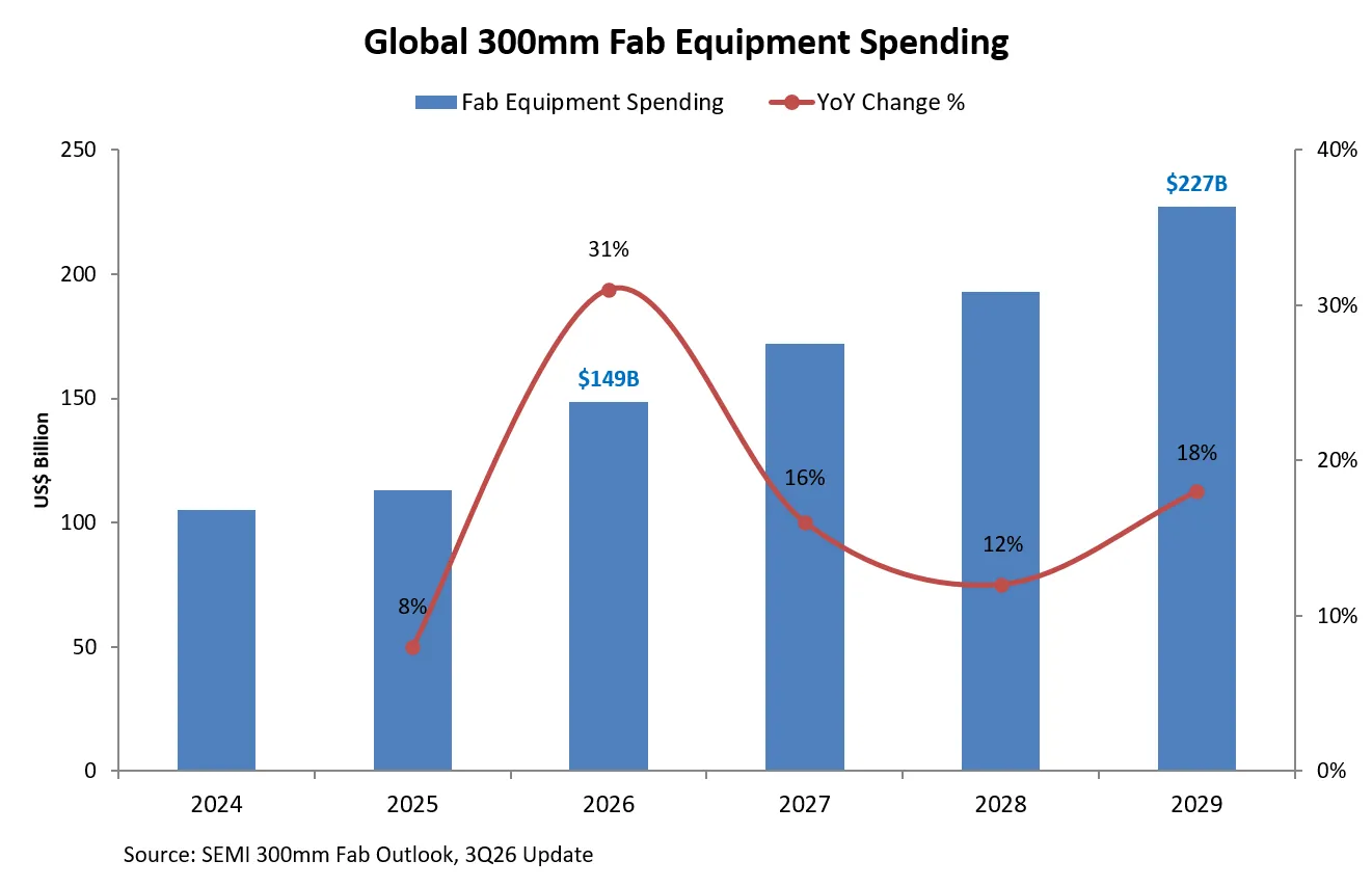
SEMICON West – SAN FRANCISCO — October 13, 2026 — Global 300mm front-end fab equipment spending is projected to reach $149 billion in 2026, up 31% year-over-year, SEMI reported today in its latest 300mm Fab Outlook. Investment is expected to continue growing at double-digit rates through 2029, reaching $227 billion.

The stronger investment trajectory is accompanied by a sustained pipeline of new 300mm fabs and production lines moving through construction and into operation. Excluding pure R&D fabs, SEMI projects 20 new 300mm fabs or lines to begin construction worldwide in 2026 and 18 in 2027. In the United States, three are projected to begin construction in 2026 and four in 2027.

“Semiconductor demand is increasingly translating into physical manufacturing expansion across the global industry,” said Ajit Manocha, SEMI President and CEO. “The latest outlook points to both stronger equipment investment and a substantial pipeline of fabs moving toward operation. This expansion will provide the manufacturing foundation needed to support AI, high-performance computing and a broad range of next-generation semiconductor applications.”


Global Fab Construction Pipeline

Across all 300mm facilities, global fab construction spending is projected to rise 23% to $47.5 billion in 2026 and another 33% to $63.3 billion in 2027, before reaching $68.4 billion in 2028. The construction activity reflects continued investment in new manufacturing capacity across leading-edge logic, memory and other 300mm semiconductor technologies.

The U.S. represents an important part of this expansion, with additional 300mm fabs and lines expected to begin construction throughout the forecast period. Equipment investment in the Americas is projected to more than double from $18.1 billion in 2026 to $40.6 billion in 2029, reflecting the region's expanding manufacturing footprint.

SEMI projects 13 new 300mm fabs or lines worldwide to begin operations or ship first silicon in 2026, increasing to 23 in 2027. 

The 3Q26 edition of the SEMI 300mm Fab Outlook reflects 166 changes across 163 fabs and lines, including 14 newly added records, since the previous report.

For more information on the report or to subscribe, please contact the SEMI Market Intelligence Team at [email protected]. Details on SEMI market data are available at SEMI Market Intelligence.  

Follow SEMI Market Intelligence

Follow SEMI 

About SEMI

SEMI® is the global industry association connecting over 4,000 companies and 1.5 million professionals worldwide across the semiconductor and electronics design and manufacturing supply chain. We accelerate member collaboration on solutions to top industry challenges through Advocacy, Workforce Development, Sustainability, Supply Chain Management and other programs. Our SEMICON® expositions and events, technology communities, standards and market intelligence help advance our members’ business growth and innovations in design, devices, equipment, materials, services and software, enabling smarter, faster, more secure electronics. Visit www.semi.org or contact a regional office to learn more.


San Francisco, Calif. — October 12, 2026 — SEMI and Semiconductor Digest today announced finalists for the Best of West award to be presented at SEMICON West 2026, October 13–15 at the Moscone Center in San Francisco, California. The Best of West Award winner will be announced at SEMICON West 2026 on Thursday, October 15, on the Smart Theater stage located inside the North Expo Hall, Lower Level Hall F.

Presented by SEMI Americas and Semiconductor Digest each year, the Best of West award recognizes innovative new products or services that are significantly advancing the electronics manufacturing supply chain or a particular manufacturing capability.

The following Best of West 2026 finalists will showcase their products on the SEMICON West 2026 show floor:

Edwards, part of the Atlas Copco Group: Ganymede Dry Pump — Booth 633
Ganymede is Edwards’ next-generation dry vacuum pump, designed for the most demanding semiconductor applications. Setting new benchmarks in productivity, operational efficiency, reliability, and sustainability, Ganymede redefines vacuum performance for harsh process environments.

Nordson Test & Inspection: SonoFlex Acoustic System — Booth 5844
The SonoFlex automated inspection tool delivers high throughput and better sensitivity for accurately locating defects in small panel-based assemblies. Scanning 2x faster than legacy systems with advanced pulser and transducer technology, panels can be inspected over the widest frequency range yet achieved in a production environment.

Siemens Industry, Inc.: Eigen Engineering Agent — Booth 5982
Eigen Engineering Agent applies purpose-built AI to industrial engineering. Working alongside Siemens TIA Portal, it plans, generates and validates PLC code, hardware configuration and HMI screens from plain-language input, delivering 2–5x faster execution and up to 80% higher solution quality.

About Semiconductor Digest
Through a mix of news, contributed articles and staff-written articles, Semiconductor Digest (www.semiconductor-digest.com), is dedicated to providing global information about the design, manufacturing, packaging and testing of semiconductors and other types of electronic devices, including MEMs, LEDs, displays, power electronics, optoelectronics/photonics, biomedical devices, solar cells, thin film batteries and flexible electronics. Semiconductor Digest consists of a website, magazine and topic-focused newsletters.

About SEMI
SEMI® is the global industry association connecting over 4,000 companies and 1.5 million professionals worldwide across the semiconductor and electronics design and manufacturing supply chain. We accelerate member collaboration on solutions to top industry challenges through Advocacy, Workforce Development, Sustainability, Supply Chain Management and other programs. Our SEMICON® expositions and events, technology communities, standards and market intelligence help advance our members’ business growth and innovations in design, devices, equipment, materials, services and software, enabling smarter, faster, more secure electronics. Visit www.semi.org, contact a regional office, and connect with SEMI on LinkedIn and X to learn more. 

 

BRUSSELS – October 6, 2026 – SEMI, the industry association advancing the global semiconductor and electronics design and manufacturing supply chain, today announced that SEMI Europe has joined the European Commission's newly established STEAM Executive Panel bringing the semiconductor industry’s perspective to discussions on skills, education, and workforce development.

The panel brings together leaders from industry, education, training, and related disciplines to provide strategic guidance on STEM sectors and innovative STEAM (Science, Technology, Engineering, Arts, and Mathematics) approaches that integrate science, technology, engineering, and mathematics with the arts and humanities. SEMI Europe joins a distinguished group of industry representatives on the panel, including SAP, LEGO Education, WindEurope, and DIGITALEUROPE. 

The STEAM Executive Panel will address the talent shortage in the semiconductor industry, with the main purpose of inspiring and educating the next generation of STEM students, from vocational education and training to higher education. 

"Europe must continue to strengthen its talent pipeline and invest in reskilling and upskilling at all levels," said Laith Altimime, President of SEMI Europe. "STEAM is critical to building the workforce of the future to achieve Europe's semiconductor ambitions. Close collaboration between industry, academia, and policymakers will be essential to developing the skilled talent needed to turn these ambitions into reality."

Over its mandate, the panel will advise on closer cooperation between education providers and businesses, strategies to raise participation in STEM and STEAM at all levels, and the development of adaptable graduates for a fast-changing world. It will also contribute to the annual STEAM Education Outlook, turning the goals of the STEM Education Strategic Plan into practical recommendations, and feed into the European Skills High-Level Board. The inaugural in-person meeting of the panel took place in Brussels on 6 October 2026. Its work can be followed through the Register of Commission expert groups.

SEMI Europe's appointment reflects its longstanding commitment to strengthening Europe's microelectronics talent pipeline. SEMI Europe will help connect education, skills development, and industry needs to ensure the next generation is equipped for careers in the semiconductor sector.

Through the Pact for Skills for Microelectronics, coordinated by SEMI Europe, industry, research hubs, education providers and NGOs have joined forces to support upskilling and reskilling, attract new talent and unlock EU and national funding. This collaboration laid the groundwork for the European Chips Skills Academy (ECSA), which now connects industry, universities and training providers across Europe, and the European Chips Diversity Alliance (ECDA), opening pathways for underrepresented talent across the semiconductor sector.

SEMI is honored to have Victoria Cummings, Senior Manager, Workforce Development & EU projects, SEMI Europe, invited to be on the STEAM Executive Panel. For more information or to get involved, contact her at [email protected].

About SEMI 

SEMI® is the global industry association connecting over 4,000 companies and 1.5 million professionals worldwide across the semiconductor and electronics design and manufacturing supply chain. We accelerate member collaboration on solutions to top industry challenges through Advocacy, Workforce Development, Sustainability, Supply Chain Management, and other programs. Our SEMICON® expositions and events, technology communities, standards, and market intelligence help advance our members’ business growth and innovations in design, devices, equipment, materials, services, and software, enabling smarter, faster, more secure electronics. Visit www.semi.org, contact a regional office, and connect with SEMI on LinkedIn and X to learn more.

 

MILPITAS, Calif. – September 22, 2026 – The Electronic Specialty Gases & Systems Conference (ESGS) 2026 will bring together leaders across the electronic gases value chain November 10-12, 2026, at the Hyatt Regency Phoenix in Arizona. Under the theme Driving Innovation Across the Electronic Gases Ecosystem, the event will explore the market dynamics, technology requirements and supply chain developments shaping semiconductor manufacturing. Registration is open.

ESGS provides a forum for executives, buyers, product managers and strategic planners from electronic gas end users, producers and equipment suppliers to exchange insights on the bulk, rare and specialty gases essential to continued electronics industry growth. The program will connect business outlooks with technical advances in vapor-phase materials, gas delivery and control, contamination management, analytical metrology and emissions reduction.

The three-day program will feature keynote presentations, policy and market updates, technical sessions and networking opportunities focused on the following areas:

  • Semiconductor market trends, public policy and the outlook for wafer fabrication equipment
  • Advanced vapor-phase materials and specialty gas applications
  • Gas systems challenges as device scaling and process complexity increase
  • Emerging deposition and etch chemistries for next-generation devices
  • Supply chain resilience across bulk, rare and specialty gases
  • Analytical metrology, contamination control, emissions abatement and sustainability

Featured speakers include:

  • Joe Stockunas, President, SEMI Americas
  • Bruce Gall, Strategic Partnerships, Google
  • Berc Kalanyan, Research Chemical Engineer, National Institute of Standards and Technology
  • Gustavo Albuquerque, PTD Gas Systems Engineer, Intel
  • David Mandia, Ph.D., Staff Process Engineer, Lam Research
  • Feng Li, Senior R&D Manager, Air Liquide Advanced Materials
  • Rachel Potter, Vice President, Specialty Gases, EMD Electronics

Mike Corbett, Managing Partner at Linx Consulting, will open the conference. Additional presentations will examine metrology program developments, advanced gas-system requirements, molybdenum deposition, solid precursor delivery, specialty-gas supply chain considerations and new chemistries for demanding semiconductor applications.

The program will also provide opportunities for participants across the electronic gases ecosystem to connect on shared technical, market and sustainability challenges. View the full ESGS 2026 agenda and register.

Follow SEMI 

About SEMI

SEMI® is the global industry association connecting over 4,000 companies and 1.5 million professionals worldwide across the semiconductor and electronics design and manufacturing supply chain. We accelerate member collaboration on solutions to top industry challenges through Advocacy, Workforce Development, Sustainability, Supply Chain Management and other programs. Our SEMICON® expositions and events, technology communities, standards and market intelligence help advance our members’ business growth and innovations in design, devices, equipment, materials, services and software, enabling smarter, faster, more secure electronics. Visit www.semi.org, contact a regional office, and connect with SEMI on LinkedIn and X to learn more. 


MILPITAS, Calif. — September 9, 2026 ─ The National Network for Microelectronics Education (NNME), a national workforce development initiative supported by the U.S. National Science Foundation (NSF) in partnership with the U.S. Department of Commerce, today announced the formation of its inaugural Industry Advisory Committee, bringing together senior leaders from the semiconductor industry, universities, and community colleges to help guide the network's national workforce strategy and strengthen the talent pipeline supporting America's growing microelectronics ecosystem.

Funded through an NSF Other Transaction Authority (OTA) award, the NNME benefits from NSF's ongoing technical collaboration and strategic guidance to help accelerate the development of innovative workforce solutions that address the nation's critical microelectronics talent needs. The SEMI Foundation serves as the Hub Operator of the NNME and is the workforce development arm of SEMI. 

Representing semiconductor manufacturers, technology companies, equipment and materials suppliers, universities, community colleges, and workforce leaders, the Industry Advisory Committee will provide strategic insight as NNME works to align with industry needs across the United States. The announcement comes as the nation experiences unprecedented investment in domestic semiconductor manufacturing and increasing demand for a highly skilled workforce capable of supporting innovation, advanced manufacturing, and long-term economic competitiveness. A national workforce landscape analysis conducted by McKinsey & Company found that the U.S. semiconductor industry could face a talent gap of approximately 127,000 to 157,000 workers by 2030, underscoring the urgency of building a coordinated, industry-aligned workforce development system.

"Building the workforce needed to support the future of microelectronics requires sustained collaboration across industry, education, and workforce partners," said Dr. Jennifer Ellis, Director of the National Network for Microelectronics Education. "The expertise represented on the committee reflects the depth of commitment across the semiconductor ecosystem, and their guidance will help ensure NNME remains closely aligned with industry needs while strengthening pathways into high-demand careers."

Through ongoing collaboration, the Industry Advisory Committee will help identify emerging workforce challenges, validate employer workforce needs, inform education and training strategies, strengthen connections across the semiconductor ecosystem, and provide strategic input on national workforce initiatives.

"The challenges and opportunities facing the semiconductor workforce are larger than any one organization can address alone," said Shari Liss, Vice President of Global Workforce Development and Initiatives at SEMI. "This Industry Advisory Committee brings together remarkable leaders who understand both the technical and workforce needs of our industry. Their collective expertise will help strengthen national collaboration and ensure we are preparing the workforce needed for the next generation of semiconductor innovation."

The inaugural Industry Advisory Committee includes:

MemberOrganization
  • Janine Rush-Byers (Chair)
  • Micron Technology
  • John Dallesasse
  • University of Illinois Urbana-Champaign
  • Katherine Dei Cas
  • Qnity
  • Elizabeth Greene
  • Lam Research
  • David Harrison
  • Columbus State Community College
  • Michael Lercel
  • ASML
  • Shari Liss
  • SEMI
  • Tara McCaughey
  • GlobalFoundries
  • Andrew Schmidt
  • AMD
  • Martin A. Schmidt
  • Rensselaer Polytechnic Institute (RPI)
  • Kwee Lan Teo
  • Samsung Semiconductor
  • Gabriela Cruz Thompson
  • Intel Corporation
  • Jared Zerbe
  • Apple


Collectively, committee members provide a broad perspective on the evolving workforce needs of the U.S. microelectronics ecosystem. The NNME will continue to expand membership to ensure broad representation across the national microelectronics ecosystem.

"The ability of the U.S. to compete globally depends on developing a workforce that can meet the pace of innovation across the semiconductor ecosystem," said Michelle Williams, Executive Director of the SEMI Foundation. "The Industry Advisory Committee represents an extraordinary group of leaders who are committed to shaping workforce solutions that are scalable, industry-informed, and built for long-term impact. Their guidance will help ensure NNME continues to create meaningful opportunities for learners while supporting the needs of the ecosystem."

Established to strengthen the nation's microelectronics workforce, NNME is building a coordinated national network that connects employers, education providers, workforce organizations, and regional partners to develop industry-aligned talent pathways. Through its Regional Nodes and national initiatives, NNME is creating a more connected and responsive workforce ecosystem capable of supporting continued semiconductor growth across the United States.

About the SEMI Foundation

The SEMI Foundation advances economic opportunity for workers while supporting the sustained growth of the global microelectronics industry. As the workforce development arm of SEMI, the Foundation works across industry, education, workforce systems, and community partners to build clear pathways into semiconductor and microelectronics careers while helping employers attract, develop, retain, and advance a highly skilled workforce. Together with SEMI’s network of more than 4,000 companies, the SEMI Foundation helps strengthen the talent pipeline powering the future of technology. Visit the SEMI Foundation online to learn more, and follow the SEMI Foundation on LinkedIn.

About NNME

The NNME is a national workforce development initiative supported by NSF in partnership with the U.S. Department of Commerce. The NNME connects industry, education, workforce systems, and regional partners through a national network designed to accelerate the development of America’s microelectronics workforce ecosystem. Visit the NNME online to learn more.

BRUSSELS – September 8, 2026 – SEMI today renews its call on European policymakers to use the proposed Chips Act 2.0 to strengthen Europe’s semiconductor competitiveness, reinforce supply chain resilience, and create the conditions needed to attract and sustain investment across the entire semiconductor value chain. SEMI outlines nine policy recommendations in its latest Position Paper on the Chips Act 2.0, aimed at helping ensure Europe remains a vital contributor to the global semiconductor ecosystem.

Several new elements in the European Commission’s draft legislative text reflect priorities raised by SEMI and its members in Europe. The proposal provides a solid basis to build on throughout the co-legislative process for further strengthening the Chips Act 2.0. 

“Europe’s semiconductor competitiveness depends on the strength of the entire ecosystem, from design and materials to equipment, manufacturing and advanced packaging,” said Laith Altimime, President of SEMI Europe. “The Chips Act 2.0 provides an important opportunity to build on Europe’s existing strengths. Our recommendations aim to ensure that the new framework delivers the speed, investment and policy certainty needed to strengthen Europe’s competitiveness and resilience.”

SEMI’s recommendations call for an expanded First-Of-A-Kind framework covering the entire semiconductor value chain, faster and more predictable investment and permitting processes, stronger industry participation in Chips Act governance, and an ambitious and balanced EU budget. The position paper also highlights the need to address Europe’s production-cost disadvantage, align demand-side initiatives with existing industry structures, establish secure and industry-led supply chain monitoring, and strengthen skills and workforce development.

SEMI will continue to engage with EU institutions, member states and industry stakeholders throughout the co-legislative process to support a Chips Act 2.0 that accelerates investment, supports all parts of the semiconductor value chain, and strengthens Europe’s role in the global semiconductor ecosystem.

SEMI Global and European Advocacy 

Visit SEMI Global Advocacy to learn more about public policy efforts and developments, or contact [email protected] to get involved. Discover how SEMI Europe Advocacy & Public Policy supports the microelectronics industry across sustainability, trade, talent, and R&D—or become involved by contacting [email protected].  

About SEMI 

SEMI® is the global industry association connecting over 4,000 companies and 1.5 million professionals worldwide across the semiconductor and electronics design and manufacturing supply chain. We accelerate member collaboration on solutions to top industry challenges through Advocacy, Workforce Development, Sustainability, Supply Chain Management, and other programs. Our SEMICON® expositions and events, technology communities, standards, and market intelligence help advance our members’ business growth and innovations in design, devices, equipment, materials, services, and software, enabling smarter, faster, more secure electronics. Visit www.semi.org, contact a regional office, and connect with SEMI on LinkedIn and X to learn more. 


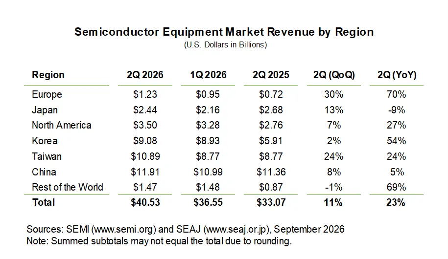
MILPITAS, Calif. – September 3, 2026 – SEMI, the industry association advancing the global semiconductor and electronics design and manufacturing supply chain, today announced in its Worldwide Semiconductor Equipment Market Statistics (WWSEMS) report that global semiconductor equipment billings increased 23% year-over-year to US$40.53 billion in the second quarter of 2026. Second quarter 2026 billings registered an 11% quarter-over-quarter growth.

The results mark a second consecutive record quarter, reflecting accelerating demand for technology and capacity solutions to support AI investments momentum as well as global buildout of AI computing infrastructure.
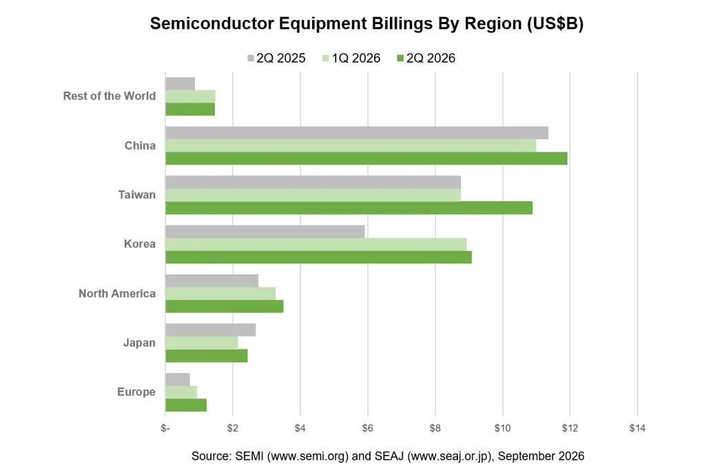
“The second consecutive quarter of record semiconductor equipment billings reflects the industry’s sustained investment in the advanced manufacturing capacity needed to support rising chip demand, particularly for AI infrastructure,” said Ajit Manocha, SEMI President and CEO. “Growth across Asia, North America and Europe underscores the global nature of this demand and the critical role of semiconductor manufacturing in enabling the next wave of AI-driven innovation.”


Compiled from data submitted by members of SEMI and the Semiconductor Equipment Association of Japan (SEAJ), the WWSEMS report is a summary of the monthly billings figures for the global semiconductor equipment industry. 

The following are quarterly billings data in billions of U.S. dollars, with quarter-over-quarter and year-over-year changes by region:


About SEMI Equipment Market Data Subscription (EMDS)

The Equipment Market Data Subscription (EMDS) from SEMI provides comprehensive market data for the global semiconductor equipment market. A subscription includes three reports: 

  • Monthly SEMI North American Billings Report, an early perspective of equipment market trends
  • Monthly Worldwide Semiconductor Equipment Market Statistics (WWSEMS), a detailed report of semiconductor equipment billings for seven regions and more than 22 market segments
  • Bi-annual Total Semiconductor Equipment Forecast – OEM Perspective, an outlook for the semiconductor equipment market

Download a sample EMDS report.

For more information about the report or to subscribe, please contact the SEMI Market Intelligence Team at [email protected]. More details are also available on the SEMI Market Data webpage.  

Follow SEMI Market Intelligence

Follow SEMI 

About SEMI

SEMI® is the global industry association connecting over 4,000 companies and 1.5 million professionals worldwide across the semiconductor and electronics design and manufacturing supply chain. We accelerate member collaboration on solutions to top industry challenges through Advocacy, Workforce Development, Sustainability, Supply Chain Management and other programs. Our SEMICON® expositions and events, technology communities, standards and market intelligence help advance our members’ business growth and innovations in design, devices, equipment, materials, services and software, enabling smarter, faster, more secure electronics. Visit www.semi.org, contact a regional office, and connect with SEMI on LinkedIn and X to learn more.

FAQ

What are the latest 2026 global semiconductor equipment billings?

SEMI reported in its Worldwide Semiconductor Equipment Market Statistics (WWSEMS) report that global semiconductor equipment billings reached US$40.53 billion in the second quarter of 2026, up 23% year-over-year and 11% quarter-over-quarter.

What are growth drivers for semiconductor manufacturing investments?

According to the SEMI WWSEMS report for the second quarter of 2026, global semiconductor equipment results reflect continued investment in advanced manufacturing capacity and technology upgrades to support rising chip demand, particularly for AI infrastructure and the global buildout of AI computing capacity.

What is the WWSEMS report and who publishes it?

The Worldwide Semiconductor Equipment Market Statistics (WWSEMS) report is a monthly SEMI market data report summarizing semiconductor equipment billings for seven regions and more than 22 market segments. It is compiled from data submitted by members of SEMI and the Semiconductor Equipment Association of Japan (SEAJ). The WWSEMS report is part of the Equipment Market Data Subscription (EMDS) from SEMI provides comprehensive market data for the global semiconductor equipment market.

TAIPEI, Taiwan – September 2, 2026 – SEMI, the global industry association connecting the electronics design and manufacturing supply chain, and Silicon Catalyst, the world's only accelerator focused exclusively on semiconductor innovation, today announced a global strategic partnership designed to accelerate innovation and strengthen connections between semiconductor hardware startups, investors, manufacturers, and technology leaders worldwide. The partnership was formalized through the signing of a Memorandum of Understanding (MOU) at SEMICON Taiwan 2026.

As the pace of technological advancement accelerates in the AI era, semiconductor companies increasingly require faster access to emerging technologies, new business models, and breakthrough innovations. Through this partnership, SEMI and Silicon Catalyst will create new opportunities for collaboration between established industry leaders and the next generation of semiconductor innovators.
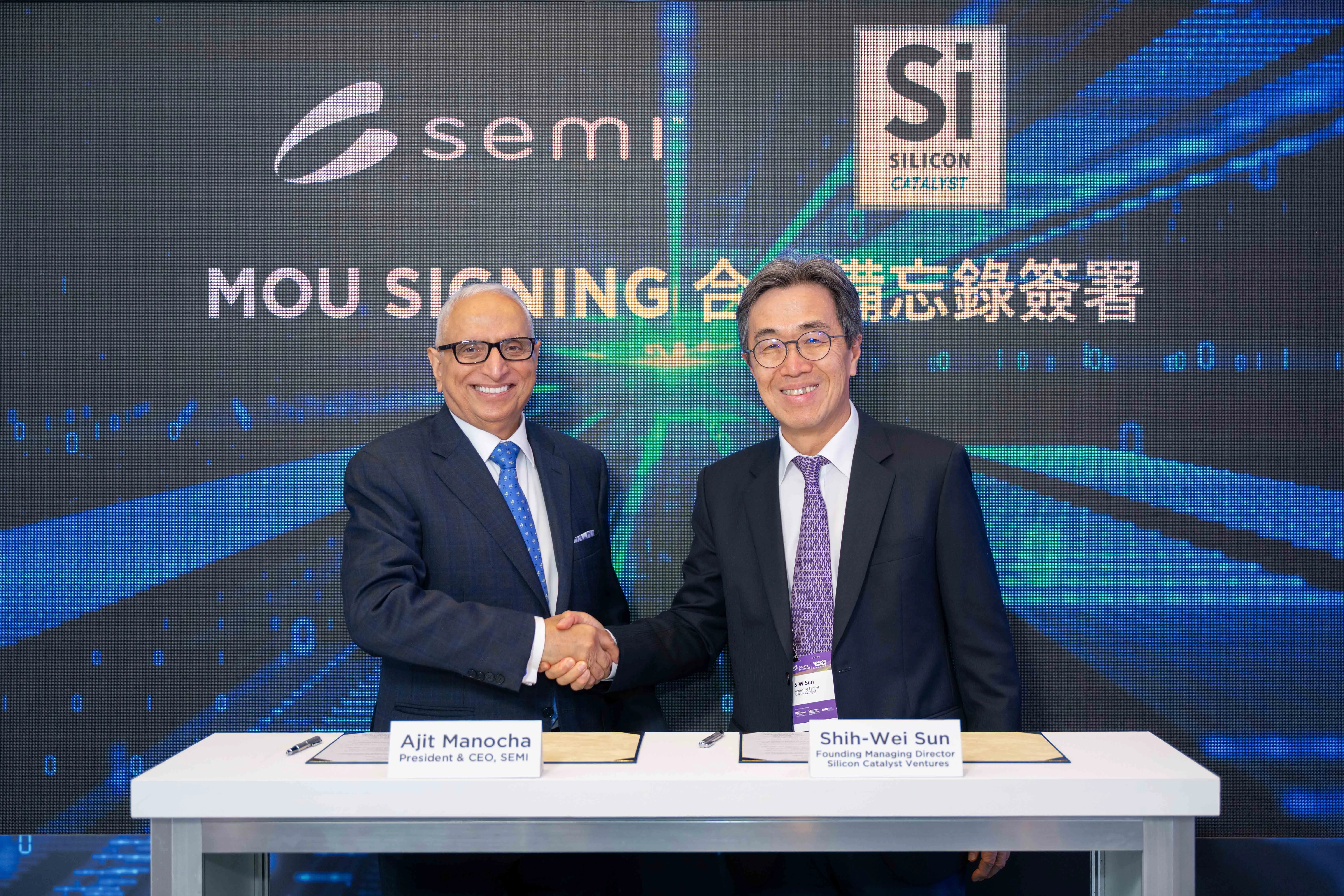
“Artificial intelligence is reshaping the semiconductor landscape and increasing the speed at which innovation must move,” said Ajit Manocha, President and CEO of SEMI. “By partnering with Silicon Catalyst, we are creating a powerful global platform that connects semiconductor startups with the industry's leading companies, investors, and manufacturing ecosystem. This initiative reflects SEMI's commitment to helping our members identify emerging technologies faster and accelerate the innovation needed to transform tomorrow.”

The partnership will initially launch through activities in Taiwan, the Americas, and Europe, with plans to extend participation opportunities to SEMI members across all regions globally. Through SEMI's global platform, members will gain access to Silicon Catalyst's portfolio of startups and innovation ecosystem, while Silicon Catalyst companies will benefit from connections to SEMI's worldwide network of member companies, investors, technology partners, and industry resources.

“This partnership brings together two organizations committed to advancing semiconductor innovation,” said Pete Rodriguez, CEO of Silicon Catalyst. “By combining Silicon Catalyst's startup ecosystem with SEMI's global industry network, we can help accelerate the commercialization of breakthrough technologies and create new opportunities for entrepreneurs, investors, and established industry leaders alike.”

As part of the collaboration, Silicon Catalyst and SEMI will co-organize startup-focused programs and events at SEMICON exhibitions worldwide, including Startup Zones, venture and investor engagement programs, and technology showcase opportunities. These initiatives will begin at the SEMICON Taiwan 2026 Silicon Startups Zone and expand to other major SEMICON events, creating a global pathway for startup engagement across the semiconductor value chain.

“Taiwan has successfully demonstrated the value of connecting startups, investors, and industry leaders through SEMI's ecosystem,” said Terry Tsao, Global Chief Marketing Officer and President of SEMI Taiwan. “This partnership builds on that foundation and creates a scalable model that can be deployed across the SEMI global network, enabling greater collaboration and innovation throughout the semiconductor industry.”

Key Takeaways on SEMI and Silicon Catalyst Startup Partnership

  • Global strategic partnership designed to accelerate innovation in the AI era
  • SEMI members gain access to Silicon Catalyst startups and innovation ecosystem
  • Silicon Catalyst startups benefit from connections to SEMI's worldwide network
  • Manifested in startup-focused activities at SEMICON exhibitions worldwide

Founded in 2015, Silicon Catalyst is the only accelerator focused exclusively on semiconductor hardware companies and has engaged with more than 5,000 semiconductor startups worldwide, resulting in over 1,500 startups applying, while supporting over 150 portfolio companies admitted. Its ecosystem includes strategic relationships with leading semiconductor companies and technology providers across the global supply chain.

The partnership supports SEMI's mission to advance the electronics manufacturing and design supply chain by fostering collaboration, accelerating innovation, and strengthening the global semiconductor ecosystem.

Silicon Catalyst Ventures Keynote at SEMICON Taiwan 2026

Shih-Wei Sun, Founding Managing Director of Silicon Catalyst Ventures and board member of Silicon Catalyst, will deliver the opening keynote address at SEMICON Taiwan, Venture Day, September 4th. He encourages any local Taiwanese startups to apply to Silicon Catalyst and will be available after his keynote address to speak with any entrepreneurial teams interested in learning about the Silicon Catalyst Accelerator.

Dr. Sun has many decades of semiconductor industry experience, including his role as CEO of UMC and founder of Silicon Catalyst Ventures. His Venture Day presentation, entitled “Accelerating Semiconductor Startups Through a Global Innovation Ecosystem” will take place at the Grand Hilai Taipei (6F).

As part of SEMICON Taiwan 2026, SEMI Venture Day is a curated platform connecting innovative startups with corporate VCs, strategic investors, and semiconductor industry leaders to foster investment and collaboration.

About SEMI

SEMI® is the global industry association connecting over 4,000 companies and 1.5 million professionals worldwide across the semiconductor and electronics design and manufacturing supply chain. We accelerate member collaboration on solutions to top industry challenges through Advocacy, Workforce Development, Sustainability, Supply Chain Management and other programs. Our SEMICON® expositions and events, technology communities, standards and market intelligence help advance our members’ business growth and innovations in design, devices, equipment, materials, services and software, enabling smarter, faster, more secure electronics. Visit www.semi.org, contact a regional office, and connect with SEMI on LinkedIn and X to learn more.  

About Silicon Catalyst – “It’s about what’s next”®

Silicon Catalyst is the world’s only accelerator focused exclusively on accelerating semiconductor hardware solutions, built on a comprehensive coalition of in-kind and strategic partners to dramatically reduce the cost and complexity of development. With a world-class network of mentors to advise startups, Silicon Catalyst is helping new semiconductor companies address the challenges in moving from idea to realization. The Accelerator supplies startups with access to design tools, silicon devices, networking, and a path to funding, banking and marketing acumen to successfully launch and grow their companies’ novel technology solutions. Having established itself as the gold standard for semiconductor hardware startups, Silicon Catalyst’s unique model has been expanded on a global basis to Israel, the UK, the European Union, Australia, Japan and Malaysia, in conjunction with government-backed regional ChipStart programs.

The Silicon Catalyst Angels (SCA) was established in July 2019 as a separate organization to provide access to seed-stage and Series A funding for Silicon Catalyst Portfolio Companies. In February of 2024, Silicon Catalyst Ventures (SCV) was launched to fund early-stage startups accepted into the Accelerator’s two-year program. Silicon Catalyst Angels and Silicon Catalyst Ventures have already made over 100 investments in semiconductor hardware companies. More information is available at www.siliconcatalyst.com.


MUNICH, Germany — September 1, 2026 — SEMICON Europa 2026, co-located with electronica, will return to Munich from November 10–13, bringing together global industry leaders, innovators, and policymakers to advance Europe’s position in the global semiconductor landscape. Registration is open.

Themed Europe’s Next Era: Navigating the Perfect Storm, SEMICON Europa 2026 centers on the increasingly interconnected relationship between technological innovation and the shifting geopolitical landscape. As global dynamics grow more complex, Europe faces both unprecedented challenges and opportunities that will define its strategic position for decades to come. This year’s program will examine how Europe can build a unified, competitive, and sustainable semiconductor ecosystem amid a fragmented global environment. 

“With more than €43 billion mobilized through the European Chips Act, and the launch of the European Chips Act 2.0 alongside major investments in manufacturing, R&D, and supply chains, Europe is strengthening its position in the global semiconductor value chain,” said Laith Altimime, President, SEMI Europe. “Europe’s semiconductor future cannot be built in isolation. By deepening collaboration across borders, connecting ecosystems, and partnering with industry, governments, and research communities worldwide, we can accelerate innovation, strengthen resilience, and build trusted global supply chains. Together, we can shape a stronger, more connected, sustainable, and future-ready European semiconductor ecosystem that contributes to and benefits from the global semiconductor community.”

At the heart of the SEMICON Europa is the CxO Summit, where visionary leaders from semiconductor powerhouses will explore the strategies and global partnerships needed to navigate the perfect storm shaping Europe’s microelectronics industry. Senior executives from CEA-Leti, Ericsson, imec, SCREEN, Schneider Electric, TRUMPF, and other leading companies across the semiconductor value chain will convene to foster insightful discussions on the pressing and emerging topics that will set the scene throughout SEMICON Europa.

Another significant focus of SEMICON Europa 2026 will be the ITF Chip into the Future — Powered by imec. Themed Building the Silicon Backbone of Europe’s AI Leadership, the program will bring together imec and leading experts to examine the chip architectures, manufacturing processes, and policy frameworks needed to establish Europe as a serious force in AI hardware, from chiplet design and sustainable fab processes to the Chips Act 2.0, the EU Chip Design Platform (EuroCDP), and the NanoIC pilot line. Industry leaders will share market perspectives on the sectors where Europe is best positioned to lead, including robotics, telecom, and next-generation compute.

Executive Forum Programs

In addition to the CxO Summit and imec ITF Chip into the Future, programs at the Executive Forum include:

Smart Mobility: Key players from across the automotive and semiconductor value chain, including OEMs, Tier 1 suppliers, semiconductor manufacturers, foundries, and technology innovators, will explore how next-generation semiconductor solutions are accelerating the evolution of smart mobility.

Electrification and Power Semiconductors: Speakers will address key advances in power semiconductors enabling the transformation toward electrification, including efficiency improvements, cost-performance trade-offs, and manufacturing technologies.

Advanced Packaging: From Strategic Imperative to Scalable Reality in Europe: Experts from Porsche Consulting and Entegris will link strategic market drivers with the materials and process innovations required for scale, concluding with a panel discussion on how Europe can bridge the gap between innovation and industrialization.

CEA-Leti: Engineering the Semiconductor Foundations of the AI Era: Researchers and technology leaders from CEA-Leti will showcase how the organization is shaping the research and technology foundations underpinning Europe’s AI semiconductor ambitions.

Materials Innovation: Speakers will highlight recent R&D initiatives, from novel materials to eco-friendly manufacturing processes, driving efficiency, performance, and sustainability across heterogeneous integration and new device architectures.

Future Computing: Experts will examine the evolving ecosystems, research initiatives, and industrial developments accelerating transformative computing technologies and their impact on the future of the semiconductor industry.

Innovation Showcase: Innovators and industry pioneers will present the latest breakthroughs in microelectronics and semiconductors through pitches and product announcements on the final day of the exhibition.

Arizona: Powering the Future of Global Semiconductor Innovation: Representatives from the Arizona Commerce Authority will explore how North America's premier microelectronics hub supports international growth through advanced manufacturing, end-to-end supply chain expansion, and transatlantic collaboration opportunities for European companies.

Building Europe's Trusted Semiconductor Corridor in the Baltic Sea Region: Speakers from Invest in Pomerania and the Nordic Chip Collaboration will explore how cross-border partnerships and regional collaboration are building resilient semiconductor supply chains across Northern Europe, positioning the Baltic Sea region as a strategic hub in Europe's semiconductor landscape.

TechARENA Programs

Sustainability, Climate and EHS: Exploring how sustainability priorities and EHS considerations are shaping semiconductor manufacturing and operations across Europe.

Spotlight to European Innovation: Showcasing how public funding instruments, including Chips JU, are working with industry to build a sovereign, secure, and quantum-safe digital future.

Skills, Diversity & the Next Generation: Exploring how training ecosystems, inclusive recruitment, and youth engagement can future-proof Europe’s chip talent pipeline.

Chips Act 2.0 – Building Europe’s Trusted Semiconductor Alliances: Assessing the evolving Chips Act 2.0 framework and how partnerships with trusted allies including the US, Japan, Taiwan, and South Korea, can strengthen Europe’s semiconductor ecosystem.

MEMS & Imaging Sensors Summit: Cutting-edge developments in MEMS and imaging technologies, with a focus on AI/ML integration and next-generation sensing applications across automotive, healthcare, and smart systems.

III-V Summit: Bringing together experts to explore the full III-V materials ecosystem — from materials innovation and electronic-photonic co-integration to manufacturing scalability and emerging applications for AI and data center infrastructure.

Smart Manufacturing: Examining how the industry is moving beyond AI experimentation to achieve measurable improvements in productivity, yield, sustainability, and operational resilience.

Future Disruptions: Insights into how advanced manufacturing, robotics, intelligent automation, and supply chain rebalancing are preparing the industry for a high-growth, execution-driven future.

NextSEMI ARENA

CHERITech'26: Experts and innovators will convene to explore how CHERI-enabled hardware architectures are advancing secure computing from innovation to large-scale deployment, as cybersecurity increasingly becomes a hardware challenge.

Start-Up Pitches: Running across three days, this program invites investors, industry leaders, and technology scouts to discover investment-ready ventures and connect with entrepreneurs shaping the future of the semiconductor industry.

SEMICON Europa × TUM Venture Labs Hackathon: The official launch of a first-of-its-kind venture-building hackathon at SEMICON Europa, uniting top talent from across Europe to form interdisciplinary teams and validate investable semiconductor product concepts directly on the show floor.

Other SEMICON Europa Highlights

Advanced Packaging Conference (APC): Leading experts from academia, industry, and government will discuss how advanced packaging innovations, from 2.5D/3D integration and chiplet architectures to next-generation materials and interconnects, are becoming a strategic enabler of system performance across AI, HPC, automotive, and edge applications.

Fab Management Forum (FMF): Senior fab managers, industry leaders, and technology pioneers will explore the roadmap toward fully autonomous fabs across three focused sessions covering competitive strategies, AI-driven smart manufacturing, and disruptive technologies shaping Europe’s semiconductor future.

SEMI Networking Night: Industry stakeholders will gather for an exclusive evening of networking with peers and key players from across the electronics sector.

20 Under 30 Award: Recognizing the brightest young leaders across Europe’s microelectronics supply chain who are driving innovation, demonstrating outstanding leadership, and making a significant impact on the industry’s future.

For more details, please visit the SEMICON Europa 2026 website and connect with SEMI Europe on LinkedIn or YouTube @SEMIEurope (#SEMICONEuropa).

Press and media partners can register for free by contacting Sitong He at [email protected].

SEMICON Europa 2026 Sponsors

Frequently Asked Questions

What is SEMICON Europa?

SEMICON Europa is SEMI’s flagship European microelectronics exhibition, bringing together leaders from across the semiconductor design and manufacturing supply chain to exchange insights, build partnerships, and advance Europe’s role in the global industry.

Why is SEMICON Europa important to the industry? 

The event reflects SEMI’s mission to connect the global electronics manufacturing ecosystem around shared priorities including innovation, supply chain resilience, workforce development and sustainability.

Who should attend SEMICON Europa?

SEMICON Europa is designed for business and technology leaders, researchers, and industry analysts from across the microelectronics supply chain who want to engage with SEMI programs, discover emerging technologies, and collaborate on solutions shaping Europe’s semiconductor future.

About SEMI

SEMI® is the global industry association connecting over 4,000 member companies and 1.5 million professionals worldwide across the semiconductor and electronics design and manufacturing supply chain. We accelerate member collaboration on solutions to top industry challenges through Advocacy, Workforce Development, Sustainability, Supply Chain Management and other programs. Our SEMICON® expositions and events, technology communities, standards and market intelligence help advance our members' business growth and innovations in design, devices, equipment, materials, services and software, enabling smarter, faster, more secure electronics.  Visit www.semi.org, contact a regional office, and connect with SEMI on LinkedIn and X to learn more.