
downloadGroupGroupnoun_press release_995423_000000 copyGroupnoun_Feed_96767_000000Group 19noun_pictures_1817522_000000Member company iconResource item iconStore item iconGroup 19Group 19noun_Photo_2085192_000000 Copynoun_presentation_2096081_000000Group 19Group Copy 7noun_webinar_692730_000000Path
Skip to main content
Default Banner Image

SEMI Press Release

ID
semi-press-release

MILPITAS, Calif. — July 13, 2026 — Electronic System Design (ESD) industry revenue increased 12.7% to $5,747.8 million in the first quarter of 2026 from the $5,098.3 million registered in the first quarter of 2025, the ESD Alliance, a SEMI Technology Coalition, announced today in its latest Electronic Design Market Data (EDMD) report. The four-quarter moving average rose 10.3%, based on a comparison of the most recent four quarters to the prior four.

A black and white image of a number

Description automatically generated with medium confidence“The electronic design automation industry continued to report strong year-over-year revenue growth in Q1 2026,” said Walden C. Rhines, Executive Sponsor of the SEMI Electronic Design Market Data report and Chief Executive Officer of Silvaco Group, Inc. “All product categories reported gains, with Computer-Aided Engineering and Semiconductor IP showing double digit growth. The Americas, EMEA, and APAC geographic regions reported growth in Q1, with double digit increases in EMEA and APAC.”

The companies tracked in the EDMD report employed 72,544 people globally in Q1 2026, a 12.6% increase over the Q1 2025 headcount of 64,403 and up 1.1% compared to Q4 2025.

The quarterly EDMD report contains detailed revenue information within the following category and geographic breakdowns. 
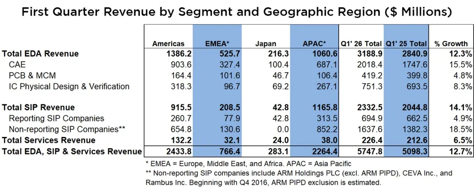
 

Revenue by Product and Application Category – Year-Over-Year Change

  • Computer-Aided Engineering (CAE) revenue increased 15.5% to $2,018.4 million. The four-quarter CAE moving average increased 13.1%. 
  • IC Physical Design and Verification revenue increased 8.3% to $751.3 million. The four-quarter moving average for the category decreased 0.9%. 
  • Printed Circuit Board and Multi-Chip Module (PCB and MCM) revenue rose 4.8% to $419.2 million. The four-quarter moving average for PCB and MCM rose 4.3%.
  • Semiconductor Intellectual Property (SIP) revenue increased 14.1% to $2,332.5 million. The four-quarter SIP moving average rose 13.7%.
  • Services revenue increased 6.5% to $226.4 million. The four-quarter Services moving average rose 11.9%.

Revenue by Region – Year-Over-Year Change

  • The Americas, the largest reporting region by revenue, procured $2,433.8 million of electronic system design products and services in Q1 2026, a 10.2% increase. The four-quarter moving average for the Americas rose 9.8%. 
  • Europe, Middle East, and Africa (EMEA) procured $766.4 million of electronic system design products and services in Q1 2026, a 17.6% increase. The four-quarter moving average for EMEA grew 10.9%. 
  • Japan’s procurement of electronic system design products and services decreased 9.9% to $283.1 million in Q1 2026. The four-quarter moving average for Japan decreased 12.4%. 
  • Asia Pacific (APAC) procured $2,264.4 million of electronic system design products and services in Q1 2026, a 17.7% increase. The four-quarter moving average for APAC grew 14.5%. 

About the EDMD Report

The ESD Alliance Electronic Design Market Data (formerly the Market Statistics Service) report presents Electronic Design Automation (EDA), SIP and Services industry revenue data quarterly. Both public and private companies contribute data to the report available from SEMI. Each quarterly report is published approximately three months after quarter close. EDMD report data is segmented as follows: 

  • Revenue by product category (CAE, IC Physical Design and Verification, SIP, PCB and MCM Layout, and Services) including numerous detailed sub-categories
  • Revenue by geographic region (Americas, EMEA, Japan and APAC)
  • Total employment at participating companies

For information about SEMI market research reports, visit the SEMI Market Research Reports and Databases Catalog. 

About the Electronic System Design Alliance

The Electronic System Design (ESD) Alliance, a SEMI Technology Coalition, is the central voice to communicate and promote the value of the semiconductor design ecosystem as a vital component of the global electronics industry. As an international association of companies providing goods and services throughout the semiconductor design ecosystem, it is a forum to address technical, marketing, economic and legislative issues affecting the entire industry. For more information about the ESD Alliance, visit http://esd-alliance.org.

Follow the ESD Alliance

About SEMI

SEMI® is the global industry association connecting over 4,000 companies and 1.5 million professionals worldwide across the semiconductor and electronics design and manufacturing supply chain. We accelerate member collaboration on solutions to top industry challenges through Advocacy, Workforce Development, Sustainability, Supply Chain Management and other programs. Our SEMICON® expositions and events, technology communities, standards and market intelligence help advance our members’ business growth and innovations in design, devices, equipment, materials, services and software, enabling smarter, faster, more secure electronics. Visit www.semi.org, contact a regional office, and connect with SEMI on LinkedIn and X to learn more.

The information supplied by the ESD Alliance is believed to be accurate and reliable, but the ESD Alliance assumes no responsibility for any errors that may appear in this document. All trademarks and registered trademarks are the property of their respective owners.
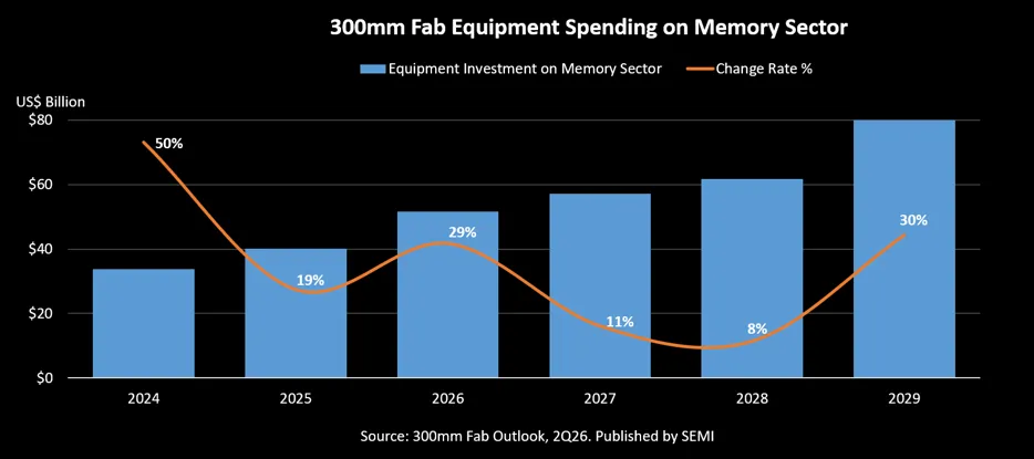

MILPITAS, Calif. – June 29, 2026 – Worldwide 300mm fab equipment investment in the memory sector is projected to surpass $50 billion for the first time in 2026, rising 29% to $52 billion before increasing another 11% to $57 billion in 2027, SEMI reported today in its latest 300mm Fab Outlook. The growth reflects continued AI-driven demand for advanced memory, supported by rising investment in AI infrastructure, data centers, and next-generation computing systems.

Looking further out, global 300mm fab equipment spending in the memory sector is expected to grow at a 19% CAGR from 2024 to 2029. Worldwide 300mm memory capacity is also projected to increase, reaching 4.1 million wafers per month in 2026 and 4.2 million wafers per month in 2027.

“Strong demand for high bandwidth memory and other advanced memory technologies is reshaping investment priorities across the semiconductor supply chain,” said Ajit Manocha, SEMI President and CEO. “As AI infrastructure expands, memory manufacturers are accelerating investments in both capacity and technology migration to support the next wave of data-intensive applications.”

Memory Segment Growth

The 2Q26 edition of the SEMI 300mm Fab Outlook includes an increased projection in 300mm fab equipment spending in the memory sector driven by continued upward capital expenditure plans among leading cloud service providers and strong demand for AI accelerators. DRAM equipment spending is expected to grow 29% to $37 billion in 2026, supported by strong HBM and DDR5 demand for GPUs and other AI accelerators. Equipment spending on 3D NAND is also projected to rise 28% to $14 billion in 2026, supported by increasing data storage requirements tied to AI deployment.

Continued investment in advanced-node DRAM and higher-layer 3D NAND is supporting a stronger memory capacity outlook, which has been revised upward in the 2Q26 edition of the SEMI 300mm Fab Outlook. Effective capacity growth, however, remains moderated by technology migration and process complexity, including advanced-node DRAM, HBM, and higher-layer NAND transitions.

The SEMI 300mm Fab Outlook lists 413 facilities and lines globally. The report reflects 155 updates and addition of 7 new fabs/lines projects since its last publication in March 2026. 

For more information on the report or to subscribe, please contact the SEMI Market Intelligence Team at [email protected]. More details are also available on the SEMI Market Data webpage.  

Follow SEMI Market Intelligence

Follow SEMI 

About SEMI

SEMI® is the global industry association connecting over 4,000 companies and 1.5 million professionals worldwide across the semiconductor and electronics design and manufacturing supply chain. We accelerate member collaboration on solutions to top industry challenges through Advocacy, Workforce Development, Sustainability, Supply Chain Management and other programs. Our SEMICON® expositions and events, technology communities, standards and market intelligence help advance our members’ business growth and innovations in design, devices, equipment, materials, services and software, enabling smarter, faster, more secure electronics. Visit www.semi.org, contact a regional office, and connect with SEMI on LinkedIn and X to learn more.  


MILPITAS, CA – June 23, 2026 — SEMI, the industry association serving the global semiconductor and electronics design and manufacturing supply chain, today announced this year’s SEMICON® West will be held October 13-15 at Moscone Center in San Francisco. Returning to the Bay Area after a successful inaugural event in Phoenix last year, this flagship exposition brings together global leaders from across the microelectronics industry to address critical industry priorities – from advanced manufacturing and supply chain resilience to sustainability and workforce development. Registration is open, with early-bird rates ending June 26. 

“As the semiconductor industry reaches the $1 trillion milestone for annual revenue this year, SEMICON West 2026 will bring the global ecosystem together at a defining moment for our industry,” said Joe Stockunas, President of SEMI Americas. “Under the theme Transform Tomorrow, the event will spotlight next-generation technologies, advance industry initiatives, and foster strategic engagements needed to help sustain long-term growth. With AI driving unprecedented demand and innovation across the value chain, we are seeing strong registrations and enthusiasm for this year’s event.”

Program highlights include:

  • CEO Summit Keynotes: Industry expert and government leader presentations offering insights into global trends and challenges reshaping the semiconductor ecosystem 
  • Focused Forums: Sessions on Design, Cybersecurity, Smart Manufacturing, Smart Mobility, and Sustainability
  • Technical Tracks: The Test Vision Symposium, Advanced Packaging and Heterogenous Integration Summit, and additional tracks covering critical areas of microelectronics innovation
  • Future Technology Sessions: Outlooks for the Future of AI Computing, Quantum Computing, NextGen Photonics, Flexible Hybrid Electronics and Smart MedTech 
  • Supply Chain Sessions: Insights on strengthening global semiconductor supply chains and strategies for building long-term resilience
  • SEMI Market Symposium and the Bulls and Bears Panel: Expert analysis and forecasts on market dynamics 
  • SEMI Workforce Development Pavilion: A dedicated space connecting job seekers with employers, featuring industry speakers, workforce initiatives, and strategies to strengthen the semiconductor industry talent pipeline 
  • SEMI U: Tailored semiconductor training courses to advance attendees knowledge and skills
  • SEMICON WestFest: An Oktoberfest-style celebration with live music, Bavarian bites and interactive experiences to bring attendees together
  • Networking Receptions: Ample opportunities to continue conversations, strengthen relationships, and forge new connections long after the show floor closes each day

For more information, please visit the SEMICON West 2026 website. For press interested in attending SEMICON West 2026, please visit our Virtual Press Office and contact Sherrie Gutierrez at [email protected]. 

Follow SEMI 

About SEMI

SEMI® is the global industry association connecting over 4,000 companies and 1.5 million professionals worldwide across the semiconductor and electronics design and manufacturing supply chain. We accelerate member collaboration on solutions to top industry challenges through Advocacy, Workforce Development, Sustainability, Supply Chain Management and other programs. Our SEMICON® expositions and events, technology communities, standards and market intelligence help advance our members’ business growth and innovations in design, devices, equipment, materials, services and software, enabling smarter, faster, more secure electronics. Visit www.semi.org, contact a regional office, and connect with SEMI on LinkedIn and X to learn more.  


MILPITAS, Calif. – June 22, 2026 – The Strategic Materials Conference (SMC) 2026 will convene materials and semiconductor leaders from July 13-15, 2026 at Hayes Mansion in San Jose, Calif. for three days of executive insights, technical discussions and networking. Under the theme, Materials Innovation in the AI Era: Powering Semiconductors to One Trillion Dollars and Beyond, industry experts will present exciting developments in this new frontier. Registration is open.

SMCSMC is the industry’s premier event focused on the materials innovations enabling semiconductor growth. The 2026 program will explore how materials advances are supporting scalable AI systems, advanced packaging, quantum computing, and emerging devices, and the industrialization of next-generation manufacturing technologies amid evolving market, geopolitical and supply chain dynamics.

SMC will open with a welcome reception on July 13 followed by two full days of keynote presentations and six sessions covering the following topics:

  • Market, Geopolitical & Economic Trends, Forecast & Outlook
  • Materials for Scalable AI Systems
  • Advanced Packaging & Materials Integration
  • From Lab to Fab: Accelerating the Industrialization of Next Generation Materials Deployment and Manufacturing
  • Quantum and the Future of Emerging Devices
  • Executive Panel: Strengthening the Supply Chain for Industry Growth

Featured keynote speakers include: 

  • Hideaki Okamoto, Mitsubishi Chemical
  • Prahalad Parthangal, Lam Research
  • Beth Adkison, Intel Corporation
  • Chuck Mattera, Avalanche Thinking

Joe Stockunas, President of SEMI Americas, and Sanjiv Bhatt of Mitsubishi Chemical Advanced Materials will welcome attendees. Additional presentations will feature industry leaders from Applied Materials, Boston Materials, EMD Electronics, Entegris, General Graphene, Georgia Institute of Technology, GlobalFoundries, Needham & Company, NVIDIA, Qnity Electronics, Rapidus Corporation, Resonac, and SkyWater Technology.

The program will also feature an executive panel examining how the industry can address supply chain constraints to support long-term resilience and growth. View the full SMC 2026 agenda and register.

Follow SEMI 

About SEMI

SEMI® is the global industry association connecting over 4,000 companies and 1.5 million professionals worldwide across the semiconductor and electronics design and manufacturing supply chain. We accelerate member collaboration on solutions to top industry challenges through Advocacy, Workforce Development, Sustainability, Supply Chain Management and other programs. Our SEMICON® expositions and events, technology communities, standards and market intelligence help advance our members’ business growth and innovations in design, devices, equipment, materials, services and software, enabling smarter, faster, more secure electronics. Visit www.semi.org, contact a regional office, and connect with SEMI on LinkedIn and X to learn more.  

MILPITAS, Calif. – June 17, 2026 – Breakthroughs in semiconductor technologies and edge AI are accelerating the rapid advancement of wearable biosensors, but despite the pace of innovation, wearables still struggle to scale beyond everyday wellness into clinically accepted healthcare solutions. To help bridge this gap, the SEMI Smart MedTech Initiative examined the systemic barriers between biosensor innovation and large-scale clinical deployment in its strategic outlook paper, Medicalizing Consumer Silicon.

“Even with today’s accelerated innovation for individual semiconductor components, poor integration is a primary barrier inhibiting the device performance required for clinical acceptance,” said Gity Samadi, Senior Director, R&D Programs at SEMI. “The core technologies that measure biomarkers in both consumer and clinical tools are similar, but the biggest differences come down to validation requirements, intended use of the device, and regulatory context. Members of the SEMI Smart MedTech Initiative authored this paper to help mitigate today’s limited alignment across stakeholders, with the goal of improving integration to create wearables that are robust enough for use in real-world healthcare settings.”

Developed through the SEMI Smart MedTech Initiative, the paper includes contributions from members including experts across the semiconductor, healthcare, medical device and academic communities. Contributors included representatives from AV, Becton Dickinson, Bosch, Brewer Science, Celtro, Intel, GlobalFoundries, Graphenea, Mayo Clinic, Medtronic, Purdue University, Rogue Valley Microdevices, STMicroelectronics, SunRay Scientific and SEMI.

The paper posits that the disparity between technological development and clinical adoption arises from several factors, including variations in biosignal acquisition, software interoperability challenges, integration of AI and data privacy, inconsistent regulatory frameworks and human factors such as comfort and consistent use. Its recommendations center on collaboration across industry sectors, academia and government to address these challenges holistically.

“Effective use of wearable devices can provide key health insights, help with diagnosis, aid in treatment planning, and track treatment effectiveness and adherence,” said Bharath Rajagopalan, Director of Strategic Marketing at STMicroelectronics. “For this to be possible, data must be trusted, clear, and usable for clinical decision making. Because the effort to acquire actionable data and streamline regulatory frameworks spans multiple disciplines and industries, the SEMI Smart MedTech Initiative is working to convene key stakeholders to address the structural issues to enable reliable and scalable adoption.”

That cross-industry input gives the paper a broader view than a single company or market segment could provide, bringing together technical, clinical, regulatory and adoption perspectives on what is needed to move wearable technologies from consumer wellness applications into clinically accepted healthcare settings.

Consumer vs. Clinical Biosensors: Case Study

Consumer wrist-worn wearables like the Apple Watch or Samsung Galaxy Watch typically rely on single-lead electrocardiography (ECG), which captures the electrical activity of the heart from one viewpoint. In contrast, FDA-cleared, Class II diagnostic wearables like the Philips MCOT or VitalConnect VitalPatch use multi-lead ECG electrodes. 

While this core difference is simple, the regulatory environment for wearable ECG devices is complex. Such regulatory challenges often arise from difficulty classifying consumer devices with functionalities that blur the line between consumer and medical use. This concern is further exacerbated by limited validation standards and interoperability frameworks, inconsistent data quality, unclear economic incentives for scalable deployment, and cybersecurity protocols that are often retrofitted instead of developed from device inception. 

Learn more about the SEMI Smart MedTech Initiative or apply for membership to help shape the next generation of wearable medical devices. The Medicalizing Consumer Silicon paper is available free of charge through the SEMI Smart MedTech Initiative website. 

About SEMI

SEMI® is the global industry association connecting over 4,000 companies and 1.5 million professionals worldwide across the semiconductor and electronics design and manufacturing supply chain. We accelerate member collaboration on solutions to top industry challenges through Advocacy, Workforce Development, Sustainability, Supply Chain Management and other programs. Our SEMICON® expositions and events, technology coalitions, standards and market intelligence help advance our members’ business growth and innovations in design, devices, equipment, materials, services and software, enabling smarter, faster, more secure electronics. Visit www.semi.org, contact a regional office, and connect with SEMI on LinkedIn and X to learn more. 


DRESDEN, Germany — June 12, 2026 — The SEMI 3D & Systems Summit, taking place June 17–19, 2026 in Dresden, will bring together the world’s foremost experts in advanced semiconductor packaging and heterogeneous systems integration. Themed Enabling Next-Gen Heterogeneous Systems Integration, the Summit will spotlight the latest breakthroughs driving innovation in AI hardware architectures, chiplet design, hybrid bonding, photonics, and AR/VR technologies. From geopolitical dynamics to system-level architectures, attendees will explore the critical role of 3D and heterogeneous integration in shaping Europe’s semiconductor future. Registration is open. 

“Dresden is reinforcing its position as one of Europe’s leading semiconductor hubs, and a central pillar driven by the European Chips Act and major investments from TSMC, Infineon, Bosch, and GlobalFoundries,” said Laith Altimime, President of SEMI Europe. “These investments are aimed at accelerating manufacturing of the next-generation semiconductor innovations in Europe advancing Europe's competitiveness, technological sovereignty, and supply chain resilience. As heterogeneous integration becomes a foundation for the future of our industry, collaboration across the value chain will be critical to ensuring Europe remains at the forefront of global innovation.”  

This year’s SEMI 3D & Systems Summit will present a broad scope of topics including:

  • Market Trends and Europe’s Technological Positioning
  • Advanced Packaging Capacity: From Lab Innovation to Fab Deployment
  • Hybrid Bonding Technologies for Die-to-Wafer and Wafer-to-Wafer Integration
  • Photonics at Scale: Co-Packaged Optics
  • Design Leadership: Chiplets & System Architecture
  • AR/VR & Wearable Intelligence

Featured Speakers

  • Atsushi Nishikawa, Co-Founder and CTO, ALLOS Semiconductors
  • Dirk Panter, State Minister for Economic Affairs, Labour, Energy and Climate Action
  • E. Jan Vardaman, President and Founder, TechSearch International, Inc.
  • Gamal Refai-Ahmed, Senior Fellow and Chief Thermo-Mechanical Architect, AMD
  • Giorgio Cesana, Director, Heterogeneous Integration Transformation Program, Global Technology R&D, STMicroelectronics
  • Harald Kuhn, Executive Director, Fraunhofer ENAS
  • Jean-Marc Yannou, Vice President, Strategy & Innovation, Murata
  • Nicolai Walter, Co-Founder and CEO, Pixel Photonics
  • Nicole Tien, Senior Technical Program Manager, ASE Europe
  • Rajesh Mandamparambil, Senior Technical Leader in Advanced Semiconductor Packaging and Heterogeneous Integration, NXP Semiconductors
  • Shripad Gokhale, Senior Principal Engineer, Semiconductor Packaging R&D, Intel Corporation
  • Volker Herbig, Vice President, BU Microsystems & Photonics, X-FAB

Networking

This year’s networking reception will take place at the Hilton Dresden Hotel on the first day of the event, and the Networking Dinner Cruise is set on a historic paddle steamer on the Elbe River, just a 5-minute walk from the Hilton Dresden Hotel.

Networking Dinner Cruise registration is reserved exclusively for 3D & Systems Summit 2026 participants.

Exhibition

The most prominent names in 3D integration and microelectronics manufacturing will showcase their latest products and technologies in the Summit's dedicated exhibition area. 

Exhibitors include: 3DiS Technologies, Adeia Inc., ASE, ASMPT, Carl Zeiss Microscopy Deutschland GmbH, Comet AG, Confovis, FAMES Pilot Line, Forschungsfabrik Mikroelektronik Deutschland (FMD), Fraunhofer IZM-ASSID, Hamamatsu Photonics Deutschland GmbH, Kistler Instrumente AG, Lam Research, LPKF Laser & Electronics SE, NanoIC Pilot Line, Plasmatreat, Precitec Optronik GmbH, SEMI Europe, SEMILAB, SET (Smart Equipment Technology), Syenta, W. L. Gore & Associates, Wooptix, and X-FAB Silicon Foundries SE.

Sponsors

Platinum: Adeia, ASE, Comet, Confovis, KLA, Lam Research
Gold: Evatec, Plasmatreat
Event: ASMPT, EV Group, imec, MKS Atotech

Call for Abstracts: 2026 Advanced Packaging Conference (APC)

Building on key topics at the 3D & Systems Summit, SEMI Europe has opened the call for abstracts for the 2026 Advanced Packaging Conference (APC), co-located with SEMICON Europa in Munich on November 10-13. Themed Power and Interconnects Innovations Enabling AI System Performance, APC 2026 will explore 2.5D/3D integration, chiplet architectures, co-packaged optics, advanced materials, AI-driven design flows, and next-generation thermal and power management across AI, HPC, automotive, and edge applications. Abstract submissions are open through July 1, 2026.

For more details, please visit the 3D & Systems Summit 2026 website and connect with SEMI Europe on LinkedIn or YouTube @SEMIEurope (#3DSummit).

About SEMI

SEMI® is the global industry association connecting over 4,000 companies and 1.5 million professionals worldwide across the semiconductor and electronics design and manufacturing supply chain. We accelerate member collaboration on solutions to top industry challenges through Advocacy, Workforce Development, Sustainability, Supply Chain Management and other programs. Our SEMICON® expositions and events, technology communities, standards and market intelligence help advance our members’ business growth and innovations in design, devices, equipment, materials, services and software, enabling smarter, faster, more secure electronics. Visit www.semi.org, contact a regional office, and connect with SEMI on LinkedIn and X to learn more.

HSINCHU, Taiwan – June 15, 2026 – SEMICON Taiwan 2026, one of the global semiconductor industry’s flagship annual events, will be held September 2-4 at the Nangang Exhibition Center in Taipei, with forums beginning on August 31 to align with International Semiconductor Week. The exhibition is expected to feature more than 1,300 exhibitors and 4,300 booths—both record highs—and attract over 100,000 professionals from 65 countries. Registration is open.

AI Reshapes the Industry as SEMI Connects the Global Ecosystem

As AI and high-performance computing (HPC) accelerate and spark a diverse range of emerging applications, the semiconductor industry is pushing the boundaries of both process scaling and system-level innovation. Advanced process nodes, advanced packaging, smart manufacturing, quantum technology, and ecosystem collaboration are key growth enablers and will be major focuses during SEMICON Taiwan 2026.

“SEMI data shows that in 2025 global semiconductor manufacturing equipment sales reached US$135.1 billion, up 15% year-over-year, while global semiconductor materials sales increased to $73.2 billion, up 6.8% year-over-year,” said Terry Tsao, Global Chief Marketing Officer and President of Taiwan, SEMI. “The semiconductor industry has carried this momentum into 2026 driven by AI, high-performance computing, advanced process technologies, and advanced packaging, with Taiwan continuing to be among the regions with the strongest growth outlook. Under the theme Transform Tomorrow, SEMICON Taiwan 2026 will bring together the global ecosystem, from wafer manufacturing, equipment, and materials to IC design, system applications, and startups to address complex industry challenges and shape the next generation of technology.”

New Zones Highlight Quantum Technology, Smart Fab, and Chiplets

SEMICON Taiwan 2026 will debut two new feature areas, the Quantum Technology Zone and Smart Fab Zone, while the Packaging Technology Area will introduce a dedicated Chiplet Pavilion.

  • Quantum Technology Zone: Spotlights superconductors, ion traps, quantum annealing, and other key pathways, showing how quantum technology is moving toward practical applications. The zone will connect government, academic, and research institutions, and international quantum computing companies.
  • Smart Fab Zone: Explores how fabs are evolving from automation toward intelligent production systems capable of sensing, decision-making, and coordination. Featured technologies include collaborative robots, humanoid robots, automated material handling systems (AMHS), and digital twins.
  • Chiplet Pavilion: Focuses on chiplet architecture for AI servers, data centers, HPC, autonomous vehicles, and 6G infrastructure. The zone will showcase advanced packaging, lithography systems, bonding technologies, and high-precision semiconductor equipment.

AI Chips, Startups, and Talent Drive Innovation

The AI Technology Zone will present the ecosystem from advanced manufacturing and AI chip design to ASIC performance and edge AI applications, highlighting the growing need for both performance and energy efficiency.

The Silicon Startups Zone, organized by SEMI with support from the National Science and Technology Council (NSTC), will expand this year in collaboration with IC Taiwan Grand Challenge (ICTGC) teams. Through showcases, startup presentations, and business matchmaking, the zone will help semiconductor startups connect with industry resources, investors, and commercialization opportunities.

The SEMI 20 Under 40 Awards return for its second year, recognizing young professionals across the semiconductor ecosystem. A new Industry–Academia Application category will further strengthen industry–academia collaboration and talent development. More than 22 forums will bring together global leaders and experts to discuss advanced packaging, memory, geostrategy, talent, sustainability, cybersecurity, and other forward-looking topics.

Registration

Registration for SEMICON Taiwan 2026 is open. Industry professionals can apply for free visitor discount codes through July 15. Super early bird registration for the international forums is also available now, offering an exclusive 30% discount for a limited time. For more details, visit the official website. 

Follow SEMI Taiwan on Facebook, LinkedIn, and Line.

About SEMI

SEMI® is the global industry association connecting over 4,000 companies and 1.5 million professionals worldwide across the semiconductor and electronics design and manufacturing supply chain. We accelerate member collaboration on solutions to top industry challenges through Advocacy, Workforce Development, Sustainability, Supply Chain Management and other programs. Our SEMICON® expositions and events, technology coalitions, standards and market intelligence help advance our members’ business growth and innovations in design, devices, equipment, materials, services and software, enabling smarter, faster, more secure electronics. Visit www.semi.org, contact a regional office, and connect with SEMI on LinkedIn and X to learn more. 

BRUSSELS – June 3, 2026 – The European Commission today officially presented the new European Chips Act 2.0, marking a major step forward in Europe’s ambition to strengthen its semiconductor competitiveness, resilience and technological sovereignty. Following the announcement, officials presented the new policy at the SEMI Europe Policy Forum in Brussels, a high-level gathering hosted by SEMI Europe bringing together leading semiconductor industry representatives, policymakers and key stakeholders from national governments.

SEMI Europe welcomes the revised framework as an important signal of the European Union’s continued commitment to supporting the semiconductor industry and securing Europe’s position in the global technology landscape. Building on the foundation established by the first European Chips Act, the updated framework aims to reinforce the entire semiconductor value chain and address the structural challenges that could impact Europe’s long-term competitiveness.

“We welcome the Chips Act 2.0’s ambition to expand the ‘first-of-a-kind’ concept, accelerate the industrial uptake of R&D, streamline permitting procedures, and stimulate demand across the semiconductor value chain,” said Laith Altimime, President of SEMI Europe. “These are critical measures to strengthen Europe’s semiconductor ecosystem, enhance technological sovereignty, and build a more resilient and globally competitive European supply chain.”

Coinciding with the Chips Act 2.0 publication, the Policy Forum once again demonstrates SEMI Europe’s role as a leading platform for dialogue between industry and policymakers at a critical moment for Europe’s semiconductor ambitions. 

“Semiconductors are a global industry, and SEMI remains committed to facilitating international collaboration essential to strengthening resilient and competitive supply chains,” said Ajit Manocha, President and CEO of SEMI. “We applaud government collaborations with industry such as the European Chips Act 2.0 and investments that build on regional strengths to accelerate innovation.”

In this regard, the SEMI Europe Policy Forum highlighted the importance of coordinated action between governments, industry and global partners to support Europe’s semiconductor ambitions. The updated Chips Act 2.0 framework reflects several priorities consistently advocated by SEMI and the broader industry, reinforcing Europe’s commitment to innovation, manufacturing and long-term competitiveness across the semiconductor ecosystem.

SEMI Europe Advocacy 

Discover how SEMI Europe Advocacy & Public Policy supports the microelectronics industry across sustainability, trade, talent, and R&D—or become involved by contacting [email protected].  

About SEMI 

SEMI® is the global industry association connecting over 4,000 companies and 1.5 million professionals worldwide across the semiconductor and electronics design and manufacturing supply chain. We accelerate member collaboration on solutions to top industry challenges through Advocacy, Workforce Development, Sustainability, Supply Chain Management, and other programs. Our SEMICON® expositions and events, technology communities, standards, and market intelligence help advance our members’ business growth and innovations in design, devices, equipment, materials, services, and software, enabling smarter, faster, more secure electronics. Visit www.semi.org, contact a regional office, and connect with SEMI on LinkedIn and X to learn more. 

MILPITAS, Calif. – June 4, 2026 – SEMI, the industry association serving the global semiconductor and electronics design and manufacturing supply chain, today announced in its Worldwide Semiconductor Equipment Market Statistics (WWSEMS) report that global semiconductor equipment billings increased 14% year-over-year to US$36.55 billion in the first quarter of 2026. First quarter 2026 billings registered a 1% quarter-over-quarter growth.

Record quarterly billings were driven by continued AI-related investment, including capacity expansion and technology upgrades supporting leading-edge logic, DRAM, and advanced packaging. 

“The strong start to 2026 reflects continued industry investment in the capacity and infrastructure needed to support AI-driven semiconductor growth,” said Ajit Manocha, SEMI President and CEO. “Record first-quarter billings highlight ongoing momentum in leading-edge manufacturing and advanced packaging.”
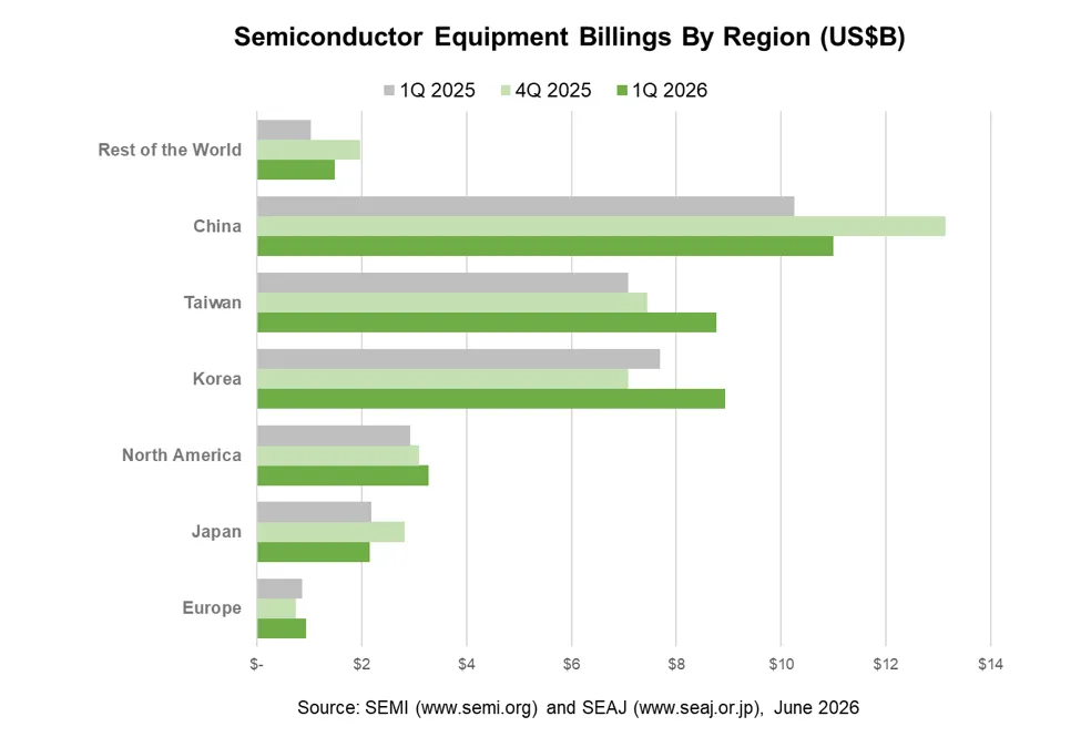
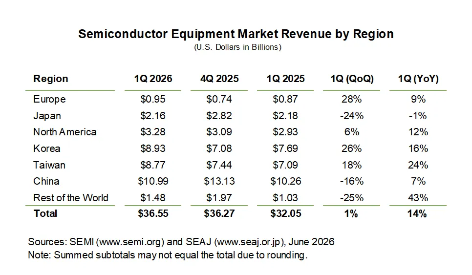
 

Compiled from data submitted by members of SEMI and the Semiconductor Equipment Association of Japan (SEAJ), the WWSEMS report is a summary of the monthly billings figures for the global semiconductor equipment industry. 

The following are quarterly billings data in billions of U.S. dollars, with quarter-over-quarter and year-over-year changes by region:


About SEMI Equipment Market Data Subscription (EMDS)

The Equipment Market Data Subscription (EMDS) from SEMI provides comprehensive market data for the global semiconductor equipment market. A subscription includes three reports: 

  • Monthly SEMI North American Billings Report, an early perspective of equipment market trends
  • Monthly Worldwide Semiconductor Equipment Market Statistics (WWSEMS), a detailed report of semiconductor equipment billings for seven regions and more than 22 market segments
  • Bi-annual Total Semiconductor Equipment Forecast – OEM Perspective, an outlook for the semiconductor equipment market

Download a sample EMDS report.

For more information about the report or to subscribe, please contact the SEMI Market Intelligence Team at [email protected]. More details are also available on the SEMI Market Data webpage.  

Follow SEMI Market Intelligence

Follow SEMI 

About SEMI

SEMI® is the global industry association connecting over 4,000 companies and 1.5 million professionals worldwide across the semiconductor and electronics design and manufacturing supply chain. We accelerate member collaboration on solutions to top industry challenges through Advocacy, Workforce Development, Sustainability, Supply Chain Management and other programs. Our SEMICON® expositions and events, technology communities, standards and market intelligence help advance our members’ business growth and innovations in design, devices, equipment, materials, services and software, enabling smarter, faster, more secure electronics. Visit www.semi.org, contact a regional office, and connect with SEMI on LinkedIn and X to learn more.

MILPITAS, Calif., May 26, 2026 — The SEMI Foundation, serving as the Hub Operator for the National Network for Microelectronics Education (NNME), today announced the launch of the first four Regional Nodes of the NNME, marking a major national milestone in the effort to build America’s microelectronics and semiconductor workforce at unprecedented scale.

Funded by the U.S. National Science Foundation Directorate for Technology, Innovation and Partnerships (NSF TIP) in partnership with the U.S. Department of Commerce and aligned with the CHIPS and Science Act, the NNME is designed to serve as national infrastructure for microelectronics talent development across the United States.  

The activation of the first Regional Nodes marks the launch of a connected national ecosystem designed to align industry demand with education, training, and career pathways that prepare new learners for high-demand careers powering the future economy.

The four Regional Nodes are:

  1. NNME Southwest, led by the Arizona Commerce Authority, serving Arizona, Southern California, Colorado, New Mexico, and Utah;
  2. NNME Pacific Intermountain, led by Boise State University, serving Idaho, Washington, Oregon, Montana, Utah, Colorado, Nevada, Northern California, and Hawaii;
  3. NNME Northeast, led by NY Creates, serving Connecticut, Delaware, Maine, Maryland, Massachusetts, New Hampshire, New Jersey, New York, Pennsylvania, Rhode Island, Vermont, and Virginia; and
  4. NNME South,  led by the University of Texas at Austin, and serving Arkansas, Mississippi, Georgia, Florida, Texas, New Mexico, Louisiana, Oklahoma, Utah, and Alabama.

Collectively, the four NNME Regional Nodes activate a national network of more than 325 performer organizations, including K-12 school districts, colleges and universities, workforce development organizations, economic development agencies, community-based organizations, and semiconductor employers working together to build stronger pathways into microelectronics careers for all Americans.

“America’s ability to lead in semiconductors depends on whether we can build and sustain the workforce needed to power innovation here at home,” said Senator Todd Young. “The National Network for Microelectronics Education represents the kind of national, industry-connected workforce strategy needed to strengthen America’s competitiveness, expand opportunity, and prepare the next generation of talent for high-demand careers in microelectronics and advanced manufacturing."

Under the NNME structure, the SEMI Foundation and NSF expect to support the four Regional Nodes with potential funding opportunities of up to $20 million per node over five years to accelerate scalable talent solutions aligned to industry demand and establish the gold standard for microelectronics education and workforce training across America.

Building the Workforce Required for America’s Semiconductor Expansion

"The launch of these Regional Nodes constitutes the activation of national infrastructure built to meet the most consequential economic and technological challenge of our time," said Shari Liss, Vice President of Workforce Development and Initiatives at SEMI and the SEMI Foundation.

“NNME is bringing together industry, educators, workforce organizations, and regional leaders to build a talent engine capable of preparing the next generation of semiconductor workers,” said Jennifer Ellis, Director of the NNME.

“This is about creating opportunity, accelerating innovation, and ensuring all Americans can participate in the future of the microelectronics economy,” Michelle Williams, Executive Director of the SEMI Foundation, added.

The announcement comes as the semiconductor industry experiences historic expansion across the country, driven by advanced manufacturing investments, supply chain growth, and increasing demand for skilled talent. A recent national landscape analysis conducted by the SEMI Foundation in collaboration with McKinsey & Company reinforces the scale and urgency of that challenge. By 2030, the United States is projected to face a shortfall of approximately 127,000 to 157,000 semiconductor and microelectronics workers.

The NNME was established to help close that gap through a nationally aligned, regionally activated strategy focused on expanding awareness, accelerating workforce readiness, modernizing education and training systems, and connecting learners directly to employment opportunities across the semiconductor ecosystem.

“America’s leadership in semiconductors depends on our ability to develop our talent,” said Erwin Gianchandani, NSF Assistant Director for Technology, Innovation and Partnerships. “The NNME represents an important investment in America’s innovation capacity, talent readiness, and long-term competitiveness. These Regional Nodes will strengthen regional ecosystems to prepare the next generation of America’s semiconductor design and manufacturing workforce.”

Connecting Industry, Education, and Workforce Systems at National Scale

The NNME Hub will work closely with employers and the NNME Regional Nodes to translate national workforce standards, technical competencies, and industry needs into scalable education and training programs tailored to regional demand.

Industry partners across the network will play a central role in shaping curriculum, validating skills, supporting work-based learning, and connecting learners directly to careers throughout the semiconductor and microelectronics ecosystem.

“Micron is proud to support the NNME and excited about what this network means for the future of American workers," said April Arnzen, EVP and Chief People Officer at Micron Technology. "Building the semiconductor workforce our country needs isn't something any one company or institution can do alone. It takes intentional collaboration across industry, education, and workforce systems. NNME is exactly that kind of partnership: a connected, national effort that creates real pathways for more Americans to access meaningful, well-paying jobs in one of the world's most important industries."

The NNME will support workforce development across the full semiconductor ecosystem, including semiconductor manufacturing, advanced packaging, facilities operations, equipment maintenance, integrated circuit design, materials, and emerging technologies.

As the NNME continues to expand nationwide, the Hub and its partners will work to strengthen shared standards, scale innovative workforce models, and build a resilient talent pipeline capable of supporting America’s long-term economic growth and technological leadership.

About NNME

The NNME is a national workforce development initiative supported by NSF in partnership with the U.S. Department of Commerce. The NNME connects industry, education, workforce systems, and regional partners through a national network designed to accelerate the development of America’s microelectronics workforce ecosystem. Visit the NNME online to learn more.

About the SEMI Foundation

The SEMI Foundation advances economic opportunity for workers while supporting the sustained growth of the global microelectronics industry. As the workforce development arm of SEMI, the Foundation works across industry, education, workforce systems, and community partners to build clear pathways into semiconductor and microelectronics careers while helping employers attract, develop, retain, and advance a highly skilled workforce. Together with SEMI’s network of more than 4,000 companies, the SEMI Foundation helps strengthen the talent pipeline powering the future of technology. Visit the SEMI Foundation online to learn more, and follow the SEMI Foundation on LinkedIn.

About NSF TIP

The NSF Directorate for Technology, Innovation and Partnerships (NSF TIP) seeks to engage all Americans in accelerating critical and emerging technologies to advance U.S. competitiveness. The directorate partners across sectors to advance three strategies – accelerating critical and emerging technology, expanding the geography of American innovation and building a competition-ready workforce. For more information about NSF TIP, visit nsf.gov/tip/latest.