PDF Solutions, Inc. (Nasdaq: PDFS) today announced it has entered into a definitive agreement to acquire secureWISE, LLC, the most widely used secure, remote connectivity solution in the semiconductor manufacturing equipment industry, from Telit IOT Solutions Inc.
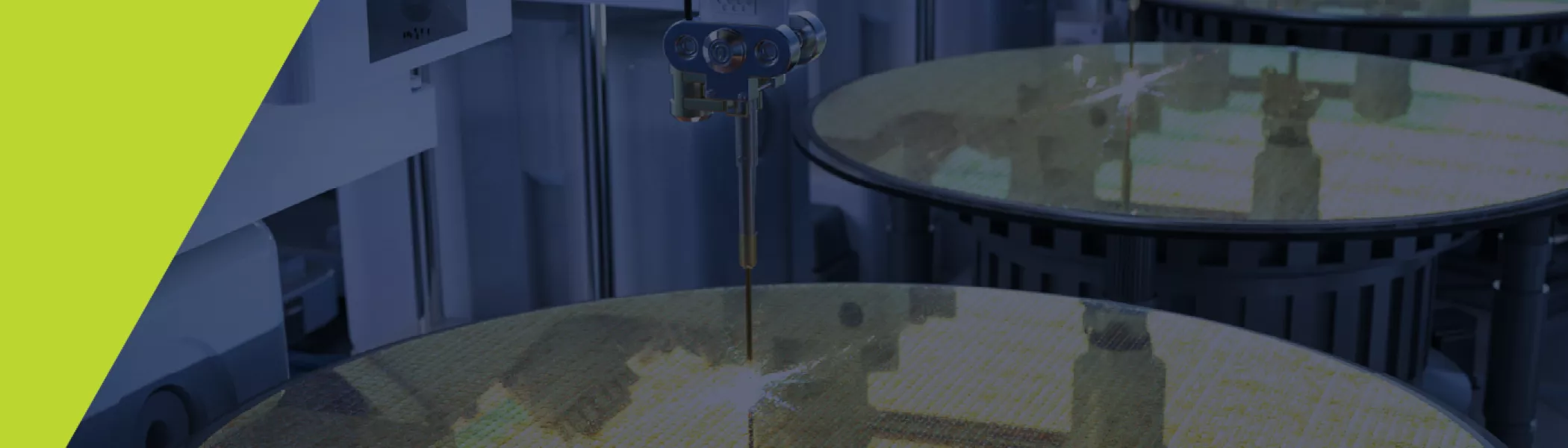
The secureWISE global network enables equipment manufacturers to bring up new equipment faster, provide operational support, and maximize the value derived from the equipment customers’ investments. It is currently used by over 100 equipment vendors to connect and control their tools located in over 190 semiconductor fabs and to manage the exchange of multiple petabytes of data annually.
PDF Solutions empowers semiconductor companies to maximize their manufacturing effectiveness. The PDF Solutions platform breaks down data silos to enable engineers to uncover critical relationships across manufacturing and design, resulting in better process control, product screening, and equipment operations.
As the semiconductor industry becomes more globally distributed, and as advanced devices rely on the integration of multiple chiplets into a single package, more collaboration and integration are required across the semiconductor industry. This collaboration needs to be executed securely with each participant controlling access to its intellectual property.
Today, secureWISE customers have built applications on top of the secureWISE network to deliver equipment analytics. PDF Solutions expects the acquisition to accelerate equipment makers’ ability to derive value from equipment data by enabling them to leverage PDF Solutions’ Exensio analytics software.
Beyond enabling equipment vendors to build equipment analytics at foundries, the acquisition of secureWISE is expected to dramatically expand the capability of PDF Solutions’ secure DEX OSAT network by allowing equipment makers, fab operators, and fabless companies to collaborate to optimize chip manufacturing and test.
“This acquisition extends PDF Solutions analytics for equipment makers and fabless to the factory manufacturing level, which allows them to generate value from AI,” said Dr. John Kibarian, President, CEO and co-founder of PDF Solutions. He continued, “We provide the leading analytics platform for semiconductor manufacturing, and with secureWISE, the PDF Solutions platform will also be able to help members of the semiconductor ecosystem collaborate through a secure, direct connection and control the manufacturing process down to the production equipment.”
Mike Dempsey, Vice President of secureWISE LLC, said, “We believe PDF Solutions is the ideal partner to accelerate secureWISE’s evolution, ensuring we remain at the forefront of industry trends and ahead of our customers’ needs. This acquisition will strengthen our ability to anticipate, pioneer, and integrate a far richer suite of security, collaboration, and analytics capabilities into our platform. As data exchange and collaboration become increasingly relevant to the semiconductor industry, this acquisition will better position secureWISE to deliver maximum long-term benefit to its customers who have invested in our platform.”
Under the terms of the definitive agreement, PDF Solutions will pay a cash amount of $130.0 million, subject to customary purchase price adjustments. The purchase price will be funded by a combination of cash on hand and $70M of new bank debt. The acquisition is subject to certain closing conditions and is expected to close in the first calendar quarter of 2025.
TD Securities (USA) LLC acted as financial advisor and Latham & Watkins LLP acted as legal advisor to PDF Solutions.
Updated Financial Outlook
John Kibarian, CEO and President of PDF Solutions, said, “Assuming the transaction closes in the first quarter of 2025, and with purchase accounting adjustments, we would expect to achieve a full year 2025 revenue growth rate between 21% to 23% on year-over-year basis. Given that, we also expect to achieve 2025 gross margin in line with our corporate gross margin, our target model 20% operating margin, and for EPS to be slightly accretive.”
Conference Call
PDF Solutions will discuss this announcement on a live conference call beginning at 3:00 p.m. Pacific Time / 6:00 p.m. Eastern Time today. To participate in the live call, analysts and investors should pre-register at: https://register.vevent.com/register/BI9abfc7eadb2245c5ba00c59922fe6c87.
Registrants will receive dial-in information and a unique passcode to access the call. We encourage participants to dial into the call ten minutes ahead of the scheduled time. The teleconference will also be webcast simultaneously on the Company’s website at https://ir.pdf.com/webcasts. A replay of the conference call webcast will be available after the call on the Company’s investor relations website. A copy of this press release will also be available on PDF Solutions’ website at News & PR Archives - PDF Solutions following the date of this release.
Forward-Looking Statements
The statements in this press release regarding the expected future financial results, benefits and synergies of the secureWISE acquisition on PDF Solution’s product offerings, and the expected closing of the secureWISE acquisition are forward looking and are subject to future events and circumstances. Actual results could differ materially from those expressed in these forward-looking statements. Risks and uncertainties that could cause results to differ materially include risks associated with: uncertainties with respect to the timing of the closing of the proposed transaction, including when and whether all conditions to closing will be satisfied; the failure of expected benefits from the proposed transaction to be realized or to be realized within the expected time period; uncertainties with respect to the future performance of secureWISE following an acquisition by PDF Solutions; PDF Solution’s ability to integrate secureWISE and its product and service offerings, the cost and schedule of new product development; continued adoption of the PDF Solution’s and secureWISE’s solutions by new and existing customers; the fact that operating costs and business disruption may be greater than expected following the public announcement or consummation of the proposed transaction; potential adverse reactions or changes to business or employee relationships, including those resulting from the public announcement or consummation of the proposed transaction; the incurrence of significant transaction costs related to the proposed transaction; unknown or understated liabilities of secureWISE; and other risks set forth in PDF Solutions’ periodic public filings with the Securities and Exchange Commission, including, without limitation, its Annual Reports on Form 10-K, most recently filed for the year ended December 31, 2023, Quarterly Reports on Form 10-Q, and Current Reports on Form 8-K and amendments to such reports. The forward-looking statements made herein are made as of the date hereof, and PDF Solutions does not assume any obligation to update such statements nor the reasons why actual results could differ materially from those projected in such statements.
About PDF Solutions
PDF Solutions (Nasdaq: PDFS) provides comprehensive data solutions designed to empower organizations across the semiconductor and electronics industry ecosystem to improve the yield and quality of their products and operational efficiency for increased profitability. The Company’s products and services are used by Fortune 500 companies across the semiconductor and electronics ecosystem to achieve smart manufacturing goals by connecting and controlling equipment, collecting data generated during manufacturing and test operations, and performing advanced analytics and machine learning to enable profitable, high-volume manufacturing.
Founded in 1991, PDF Solutions is headquartered in Santa Clara, California, with operations across North America, Europe, and Asia. The Company (directly or through one or more subsidiaries) is an active member of SEMI, INEMI, TPCA, IPC, the OPC Foundation, and DMDII. For the latest news and information about PDF Solutions or to find office locations, visit: https://www.pdf.com.
Headquartered in Santa Clara, Calif., PDF Solutions also operates worldwide in Canada, China, France, Germany, Italy, Japan, Korea, Sweden, and Taiwan. For the Company’s latest news and information, visit https://www.pdf.com.
About secureWISE
The secureWISE platform enables secure and controlled remote connectivity, collaboration and service enablement in the semiconductor industry. The secureWISE suite of products and services is designed to give OEM suppliers role-based, real-time and on-demand access to their equipment that is installed at the production facilities of their customers, to deliver valuable operational insights, mission-critical performance, substantial time and cost savings, and new service revenue opportunities. As the only remote access tool built around the ISMI guidelines, secureWISE is installed in over 90% of the world’s 300mm semiconductor fabs and also numerous solar and chemical plants across the globe. https://www.telit.com/iot-platforms-overview/telit-securewise/
PDF Solutions and the PDF Solutions logo are trademarks or registered trademarks of PDF Solutions, Inc. and/or its subsidiaries in the United States and other countries. Other trademarks used herein are the property of their owners.


 ISS Europe 2025 will feature featured speakers addressing key unprecedented challenges and opportunities in the semiconductor industry. Topics will focus on the role of artificial intelligence (AI) in shaping the industry, strategies to strengthen Europe’s semiconductor supply chain resilience, sustainability, and innovative approaches to workforce development. Industry executives, market analysts, economists, and policymakers will convene to discuss the latest industry trends and advancements.