This event has sold out!
If you would like to be put on the waitlist, please click on the interest form.
Suggested Hotels:
Embassy Suites by Hilton Milpitas Silicon Valley
901 East Calaveras Boulevard
Milpitas, CA 95035
(408) 942-0400
Courtyard by Marriott Milpitas Silicon Valley
1480 Falcon Dr.
Milpitas, CA 95035
(408) 719-1966
Milpitas, CA
United States
Morning, Day 1: June 11, 2025
Registration & Breakfast
Session #1 – Overview of Agentic AI in Semiconductor Manufacturing
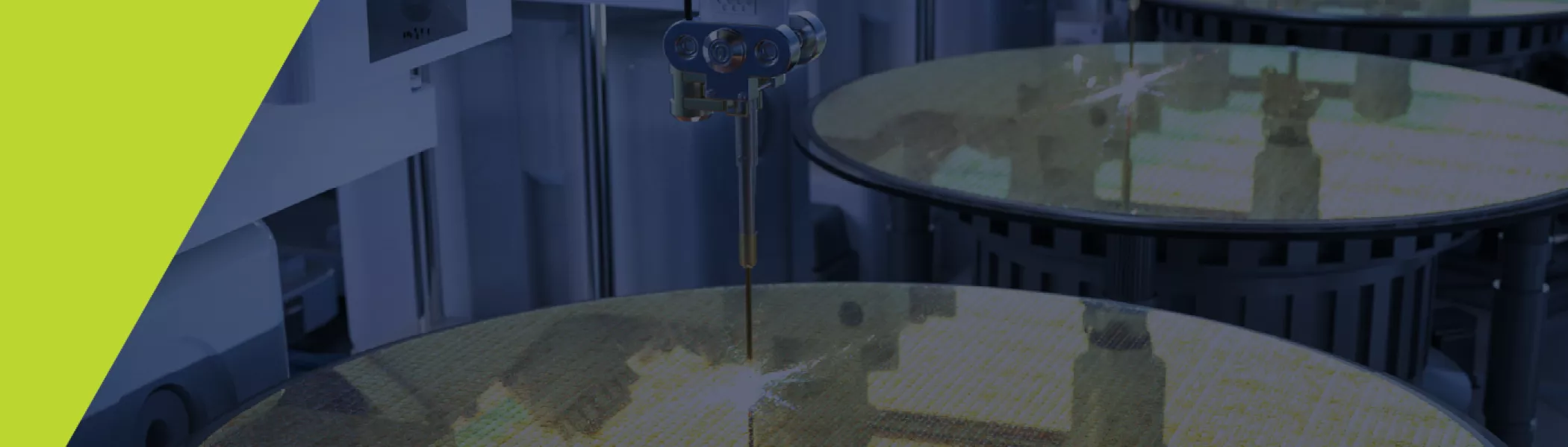
The session introduces Agentic AI and its applications in semiconductor manufacturing, addressing critical challenges like defect detection, yield enhancement, and process variability. Through real-world case studies, it will demonstrate how AI-driven solutions can significantly improve in fab efficiency and accuracy. The discussion will highlight the transformative potential of Agentic AI in optimizing semiconductor production, setting the stage for deeper exploration in future discussions.

Welcome Remarks

Keynote Speaker - Agentic AI: Opportunity, Technologies & Risks

Keynote Speaker - Industrial Co-Pilots and Agentic AI
Coffee Break

Real World Manufacturing Applications

Leveraging Physics-Based Digital Twins for Efficient Semiconductor Manufacturing

Sponsor Presentation - SEEQ

Panel Discussion
Lunch
Afternoon, Day 1: June 11, 2025
Session #2 – Process Control with Agentic AI
The session will focus on leveraging Agentic AI for process optimization, including Smart FDC, YMS, ML Ops, and recipe optimization. Key topics will include look-ahead scheduling, line balancing, virtual metrology, and smart inspection strategies. Energy and gas management strategies are highlighted alongside AI-driven sampling optimization. Practical methods for seamlessly integrating AI into existing manufacturing systems will be explored, with an emphasis on streamlining operations to achieve autonomous manufacturing.

Keynote Speaker - Agentic AI in Process Control: A Practical Roadmap for Fab Transformation

Autonomous Process Control & Optimization

Purpose-Specific Automatic Learning Machine for Fab-Wide Virtual Metrology
Coffee Break

AI Agents as Troubleshooting Partners & Knowledge Managers

Automate the Mundane or Achieve the Incredible (or Both): The Dawn of Agents in the Fab
Panel Discussion

SEMI Smart Mfg NA Chapter introduction with the Smart Mfg Roadmap pyramid
Networking Dinner Reception
Sponsored by SEEQ
Morning, Day 2: June 12, 2025
Registration & Breakfast
Session #3 – Predictive Maintenance in Semiconductor Fabs
The session will highlight the use of Agentic AI for equipment health monitoring and predictive maintenance in fabs and sub-fabs, exploring benefits such as cost savings, improved uptime, and enhanced operational efficiency. Key topics will include smart maintenance, prognosis health monitoring, anomaly detection and techniques for estimating the remaining useful life (RUL) of equipment. The session will emphasize AI's role in optimizing maintenance practices.

Keynote Speaker – Agentic AI for Industry 4.0 (Smart Manufacturing)

From Engineer Assistant to Virtual Engineer

AI Agents for Factory Maintenance: Using Factory Data for Automated Decisions
Coffee Break

Predictive Maintenance in Semiconductor Fabs
Enhancing Predictive Maintenance Algorithms through Equipment Failure Analysis

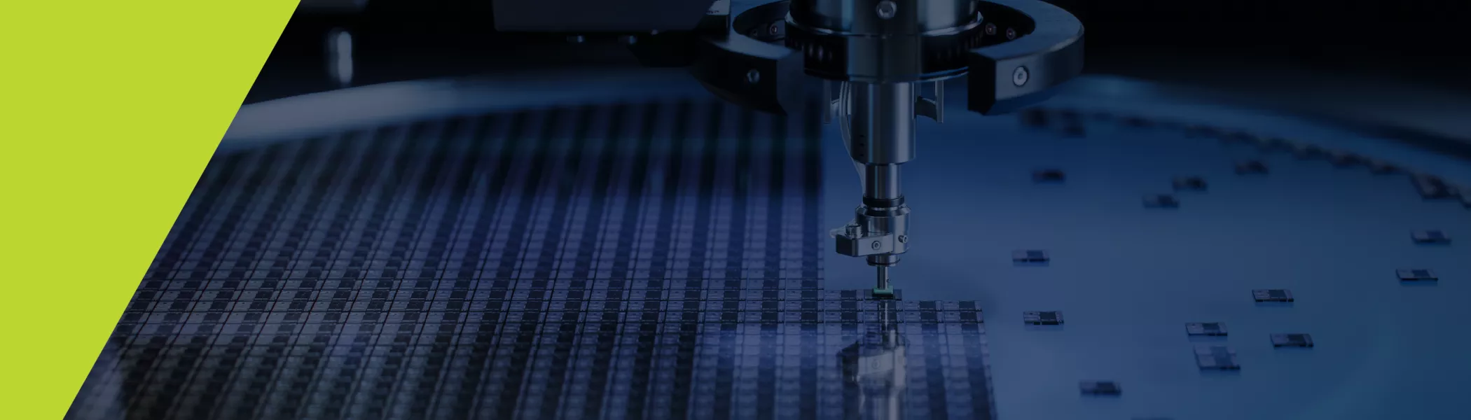
AI agents in a few-shot learning for autonomous fault detection and prediction in semiconductor fabrication


Building observable and scalable Multi Agent Workflows for Predictive Maintenance
Lunch
Afternoon, Day 2: June 12, 2025
Session #4 – Data Integration & Supply Chain
Efficiency in supply chains can be significantly enhanced by deploying AI agents for fundamental tasks such as factory-level planning, floor scheduling, real-time dispatching, and monitoring manufacturing processes at remote or contract facilities. These agents can quickly issue alerts for variations in yields or shipping schedules, taking corrective actions, such as expediting or rerouting shipments to prevent delays. Given the complexity of extended global supply chains—especially those involving multiple fabrication, assembly, and testing cycles compounded by chiplet production and advanced packaging—AI agents substantially improve coordination and operational efficiency.

Agentic AI in Factory Planning & Scheduling Digital Twin Solutions

Data Integration & Supply Chain - Challenges & Opportunities

Orchestrating Data for Agentic AI: Transforming Semiconductor Manufacturing
Coffee Break

Agentic AI and Advanced Optimization for Production Planning and Scheduling

Multi-Agent Reinforcement Learning and Tool Processing Time Prediction for Optimized Semiconductor Manufacturing
Wrap-Up
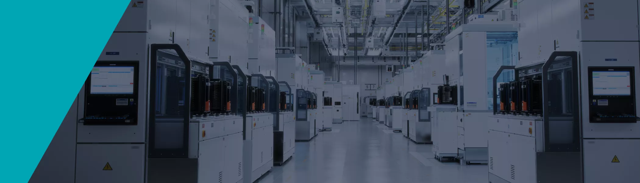
This workshop will delve into the transformative impact of Agentic AI on semiconductor manufacturing. Agentic AI refers to AI Systems that can act with a certain level of autonomy and are capable of making decision to achieve specific objectives. In this workshop, the focus will be on how Agentic AI can revolutionize various stages of semiconductor manufacturing. Aligned with SEMI Smart Manufacturing’s roadmap vision Agentic AI systems are poised to significantly enhance areas such as process control (FDC, APC, etc.), Virtual Metrology, predictive maintenance, and more - including reducing energy and material usage. This workshop will provide an in-depth look as to how Agentic AI can optimize factory systems and improve outcomes. It's ideal for semiconductor manufacturing professionals, AI enthusiasts, and business leaders seeking to leverage Agentic AI for a competitive edge.