downloadGroupGroupnoun_press release_995423_000000 copyGroupnoun_Feed_96767_000000Group 19noun_pictures_1817522_000000Member company iconResource item iconStore item iconGroup 19Group 19noun_Photo_2085192_000000 Copynoun_presentation_2096081_000000Group 19Group Copy 7noun_webinar_692730_000000Path
Skip to main content
Default Banner Image

Vietnam

ESPOO, Finland, 23rd November 2020 – Picosun Group, the leading supplier of AGILE ALD® (Atomic Layer Deposition) thin film coating solutions, partners with prominent Chinese hospitals and researchers to apply medical ALD technology for safer surgical procedures.

Picosun’s biocompatible ALD coatings will be applied on electrosurgical equipment (electrotomes) to improve their performance, safety, and service life.

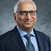
“It’s great to collaborate with a company such as Picosun to develop solutions for safer and more patient-friendly surgeries. Picosun is the leader in medical ALD solutions. The company has extensive process portfolio for biocompatible ALD materials and their equipment are at use at several medical equipment manufacturers around the world. In China, Picosun is the market leader with numerous PICOSUN® ALD systems installed throughout the country. We have strong trust that this collaboration will result in disruptive new innovations and novel solutions for surgical equipment,” says Longsheng Lu, Professor of South China University of Technology.

Electrotome utilizes high temperature to cut and separate tissue, with simultaneously coagulating blood, and it’s a standard equipment replacing traditional mechanical scalpels in many operations. Tissue and blood sticking and burning on the electrotome blade is a serious problem because the crusted blade risks increased bleeding, tissue damage, tearing and scarring, thus making the patient’s healing time longer. Smoke from the burning tissue may also hinder the surgeon’s vision and increase the risk for error during delicate procedures such as cardiac or neurosurgery.

This far, there hasn’t been a working solution in the market to overcome this problem. ALD technology can potentially provide this solution and thus improve patient safety, wound quality and healing time. ALD forms ultra-thin, pinhole-free coatings with unmatched conformality over the smallest microscale details of the surface, and the ALD process can be performed at moderate temperatures so the method is suitable also for sensitive materials. Deposited over special anti-adhesive micropatterning of the electrotome blade, biocompatible ALD film prevents blood and tissue from sticking to the blade.

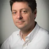
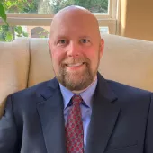
“We are happy to extend our PicoMEDICAL™ technology to a yet new healthcare application, and to work with top tier Chinese hospitals and scientists to qualify our solutions in everyday use. ALD is revolutionizing the medical field right now, just like it did to semiconductor industries over a decade ago. We at Picosun want to use our extensive ALD know-how to develop solutions to improve people’s health and quality of life, which is why medical ALD is one of our key markets for the future,” continues Dr. Jani Kivioja, CTO of Picosun Group.

Picosun provides the most advanced AGILE ALD® (Atomic Layer Deposition) thin film coating solutions for global industries. Picosun’s ALD solutions enable technological leap into the future, with turn-key production processes and unmatched, pioneering expertise in the field – dating back to the invention of the technology itself. Today, PICOSUN® ALD equipment are in daily manufacturing use in numerous leading industries around the world. Picosun is based in Finland, with subsidiaries in Germany, USA, China mainland and Taiwan, Singapore, Japan and South Korea, offices in India and France, and a world-wide sales and support network. Visit www.picosun.com.

The project “Design of anti-adhesive surface modified with bionic microstructures and ALD coatings and its application on surgical electrotomes” is carried out in collaboration with SCUT (South China University of Technology), PLAGH (General Hospital of the People's Liberation Army), Guangdong Provincial People's Hospital, and Guangzhou First People’s Hospital. The project will start on 1st December 2020 and continue for 3 years. The project is partially funded by Business Finland.

More information:
Dr. Jani Kivioja
CTO, Picosun Group
Tel: +358 46 922 8804
Email: [email protected]
Web: www.picosun.com

Registration

Webinar Image

Open to all. 

Not able to attend? Register anyway. We'll send you a link to view the webinar at your own convenience. 

Webinar Image
Belgium China France Germany Ireland Italy Japan Malaysia Russia Singapore South Korea Taiwan United States Vietnam Listen Now CEO Webinar 6 2 Executive
ase group logo
KLA

This SEMI CEO Series Webinar will bring you expert analysis of the outcome of the U.S. presidential election on current geopolitical tensions and the corresponding impact on the global microelectronics supply chain. SEMI President and CEO Ajit Manocha invites you to join us for an opening presentation from Eurasia Group on the post-election world and US-China trade, focusing on implications for the semiconductor and the bigger technology sector.

A panel discussion with industry CEOs from multiple regions and segments will provide their perspectives to the analysis, addressing the role industry executives can play in easing trade tensions and providing insights on navigating the current geopolitical environment.

United States

4:30 pm
Ajit formal photo Square 500px
Ajit Manocha
CEO and President
SEMI

Welcome & Opening Remarks

4:35 pm
Joe Pasetti, SEMI
Joe Pasetti
VP, Global Advocacy & Public Policy
SEMI

SEMI Global Advocacy Priorities

4:40 pm
Gerald Michael Butts
Gerald Butts
Vice Chairman
Eurasia Group

Macro Overview on the Post-Election World and US-China Trade

4:55 pm
Kevin Allison
Kevin Allison
Director, Geotechnology
Eurasia Group

Implications for Semiconductor and Overall Tech Industry

5:10 pm
James Andrew Lewis
Moderator

CEO Panel

James Andrew Lewis
Senior VP and Director, Strategic Technologies Program
Center for Strategic and International Studies (CSIS)
Biography

Mitsunobu Koshiba Photo
Panelist

Mitsunobu Koshiba
Chairman of the Board
JSR
Biography

Bertrand Loy
Panelist

Bertrand Loy
President and CEO
Entegris
Biography

Dr. Steve Schwartz
Panelist

Dr. Stephen Schwartz
President and CEO
Brooks Automation
Biography

Tien Wu 575 pixel
Panelist

Dr. Tien Wu
Director and CEO
Advanced Semiconductor Engineering, Inc. (ASE Group) and USI
Biography

5:45 pm

Q&A

5:58 pm

Closing Remarks

- 12:00 pm - 12:00 pm Off Add to Calendar Disabled America/Los_Angeles
Event format

ESPOO, Finland, 19th October 2020 – The Chairman of the Board and founder of Picosun Group, Mr. Kustaa Poutiainen, has been awarded as Finland’s Entrepreneur of the Year 2020. Mr. Poutiainen received the National Entrepreneur Award in the annual meeting of the Federation of Finnish Enterprises in Jyväskylä on 17th October. The award is given every year to four Finnish entrepreneurs as a recognition of exceptional entrepreneurship.

Picosun provides ALD (Atomic Layer Deposition) thin film coating solutions to global microelectronics and other industries. ALD was invented in Finland in 1974 by Picosun Board Member Dr. Tuomo Suntola, who in 2018 received the Millennium Technology Prize in recognition of his invention. ALD is a mature, key enabling technology in today’s semiconductor manufacturing, realizing the development of modern microelectronics according to the Moore’s Law. ALD is expanding rapidly to other fields of industry as well, and it is expected to bring a fundamental disruption especially to healthcare technologies, where Picosun’s PicoMEDICAL™ solutions have already enabled several new innovations.

“Even if we had great premises to start manufacturing ALD equipment, not everyone believed in us in the beginning. Our personnel did and showed what they are capable of. It has taken us to a path of excellent growth,” says Poutiainen.

Picosun’s first customers, when the company entered the ALD business in 2004, were universities and research institutes. Now, the world’s leading electronics manufacturers and other companies turn to Picosun when they need the most advanced thin film coating technology to stay spearheading their own industries. Even in the middle of the global pandemic, Picosun’s turnover is expected to grow 50%, which is remarkably higher than the market’s average of 15%.

“Since day one, our vision was to be the best in the world. We have already achieved this with our R&D ALD tools, and now we are heading further. We invest a significant amount of our turnover in development of our ALD solutions and our personnel so that we can always exceed the expectations of our customers. It is an honor to receive the National Entrepreneurship Award of Finland, and it is an honor to be a part in steering Picosun towards the future, which looks very bright indeed,” continues Poutiainen.

“The whole Picosun team wants to congratulate our Chairman, Kustaa Poutiainen, on this prestigious award. We are very proud of his significant contributions and role in enabling the international breakthrough of Finnish originated ALD technology. I am sure that the entire global ALD community appreciates his efforts and joins our congratulations,” summarizes Mr. Jussi Rautee, CEO of Picosun Group.

More information:
Mr. Jussi Rautee
CEO, Picosun Group
Tel: +358 50 345 4457
Email: [email protected]
Web: www.picosun.com

ESPOO, Finland, 6th October 2020 – Picosun Group, the leading supplier of AGILE ALD® (Atomic Layer Deposition) thin film coating solutions for global industries, strengthens its position in power electronics market with several cluster ALD system sales to prominent manufacturers in Europe, USA and Asia.

“Power electronics is an important, fast growing market for Picosun. ALD has potential to solve various challenges manufacturers are facing in this field, and our solutions have enabled our customers to create significant added value in terms of device quality and throughput. At Picosun, we have developed several turn-key production ALD solutions specifically for 4-8 inch wafer markets such as power devices. Especially our cluster ALD systems, such as the PICOSUN® Morpher which we launched last year, have been extremely well received by our customers,” says Juhana Kostamo, Head of Customer Solutions/Deputy CEO of Picosun.

Power components are crucial in a wide range of applications from consumer electronics to transportation, energy production and distribution, including renewables such as wind and solar power generation. These components are typically manufactured on 4-8 inch compound semiconductor wafers such as GaN and SiC. These materials provide various benefits compared to pure silicon, for example higher electron mobility, higher threshold voltage, and ability to operate at higher temperatures. Challenges do exist, however, as GaN and SiC power devices are prone to high interface trap density (leading to parasitic currents and reduced electron mobility) and gate leakage current, and poor threshold voltage stability.

Interface trap density can be reduced by combining pre-cleaning methods with high permittivity, large bandgap insulators. High quality, defect-free high-k dielectric layers such as Al2O3, AlN or ZrO2 etc. are key in reducing power devices’ gate leakage current and to improve electron mobility and threshold voltage stability. A good example here are GaN-based HEMTs (high electron mobility transistors), which are important in various large scale practical applications, and which require efficient gate insulation and surface passivation to achieve optimal functionality.

ALD stands as a superior deposition method here compared to other thin film coating technologies such as PECVD, as ALD produces the most conformal, uniform, and defect-free films with accurate, digitally repeatable thickness control and sharp interfaces. With the right selection of ALD deposition equipment, even multilayer processing is possible i.e. various functional material layers and/or stacked films/nanolaminates can be manufactured in one process run.

PICOSUN® Morpher is a disruptive ALD production platform designed for up to 8 inch wafer industries such as power electronics, MEMS, sensors, LEDs, lasers, optics, and 5G components. Morpher’s operational agility makes the system adaptable to various and changing manufacturing needs, on all business verticals from corporate internal R&D to production and foundry manufacturing, where both the end products and/or customers’ requirements may change rapidly. Morpher can handle several substrate materials, batch and substrate sizes, and ALD materials with leading process quality. Multilayer deposition is possible, and cluster design allows integration of also other processing units such as pre-clean, RIE etc. for fully automated, high throughput continuous vacuum operation.

“In its versatility and transformability, Morpher is the epitome of our principle ‘Agile ALD’. Innovation, constant development and improvement of our ALD solutions to enable our customers’ success is our driving force at Picosun. This applies also to Morpher platform and we have some truly exciting additions to this product family coming in the near future,” summarizes Kostamo.

About Picosun
Picosun provides the most advanced AGILE ALD® (Atomic Layer Deposition) thin film coating solutions for global industries. Picosun’s ALD solutions enable technological leap into the future, with turn-key production processes and unmatched, pioneering expertise in the field – dating back to the invention of the technology itself. Today, PICOSUN® ALD equipment are in daily manufacturing use in numerous leading industries around the world. Picosun is based in Finland, with subsidiaries in Germany, USA, Singapore, Taiwan, China, Korea and Japan, offices in India and France, and a world-wide sales and support network. Visit www.picosun.com.

More information:
Juhana Kostamo
Head of Customer Solutions/Deputy CEO, Picosun Group
Tel: +358 50 3699 565
Email: [email protected]
Web: www.picosun.com

ESPOO, Finland, 24th September 2020 – Picosun Group, the leading supplier of AGILE ALD® (Atomic Layer Deposition) thin film coating technology, reports excellent results in UVC (ultraviolet-C) LED performance, achieved with the company’s ALD solutions.

Excellent reliability and lifetime improvements of UVC LEDs have been obtained at Picosun’s customer and collaboration partner site, National Chiao Tung University (NCTU), Taiwan, using passivation and barrier films deposited with PICOSUN® ALD equipment(*). ALD passivation layer could potentially replace the expensive hermetic seal package of the LEDs and thus lower the costs of the final device.

“We have used Picosun’s ALD technology already for years with great success. Our PICOSUN® ALD equipment yields superior quality films which has helped us to achieve several breakthroughs in our LED research. Picosun has local presence in Taiwan and we appreciate the prompt response of their customer support if we ever have any issues. At the phase when R&D results are to be ramped up to industrial-level production, the scalability of Picosun’s ALD technology is a huge benefit,” comments Professor Hao-Chung Kuo from NCTU.

In order to reach maximum light output and long operating lifetime, LED chips require surface passivation to eliminate parasitic currents caused by traps and defects. Also barrier coating is typically needed as LED materials are sensitive to moisture. ALD is an ideal technique to manufacture both the passivation and barrier films – and when the LED size diminishes to micrometer dimensions, the only coating method capable of producing high enough quality films on the required minuscule scale. Ultra-thin, pinhole-free ALD films do not suppress the LED light intensity and they provide reliable protection against ambient conditions, whereas their superior conformality ensures no thickness variations between the facets of the LED chip. Thickness variations, typical side effect of other coating methods, can potentially lead to uneven distribution of film stress or thermal expansion behavior and risk physical damage of the chip.

Short-wavelength UVC radiation destroys bacteria and viruses so UVC LED technology is particularly topical now during the still ongoing COVID-19 pandemic. Small, lightweight LEDs enable versatile design of portable, compact disinfecting equipment, they consume less power than other UVC sources, they are durable, and they pose no risk of hazardous material leaks such as e.g. mercury lamps.

“We are happy of the achievements of Professor Kuo’s group at NCTU, and how Picosun’s ALD technology has helped them to achieve their goals in UVC LED development. Our long-term collaboration and networking with both the academia and prominent industries in this field gives us the perfect synergy advantage to facilitate implementation of these solutions in industrial manufacturing,” says Mr. Edwin Wu, CEO of Picosun Asia Pte. Ltd.

(*) UVC LED with 50 nm ALD Al2O3 passivation and normal LED packaging (no hermetic seal) maintained 80% of its original efficiency even after 500 hours environmental test at 85% humidity and 85 oC temperature.

About Picosun
Picosun provides the most advanced AGILE ALD® (Atomic Layer Deposition) thin film coating solutions for global industries. Picosun’s ALD solutions enable technological leap into the future, with turn-key production processes and unmatched, pioneering expertise in the field – dating back to the invention of the technology itself. Today, PICOSUN® ALD equipment are in daily manufacturing use in numerous leading industries around the world. Picosun is based in Finland, with subsidiaries in Germany, USA, Singapore, Taiwan, China, Korea and Japan, offices in India and France, and a world-wide sales and support network. Visit www.picosun.com.

More information:
Mr. Edwin Wu
CEO, Picosun Asia Pte. Ltd.
Tel: +358 40 480 3449
Email: [email protected]
Web: www.picosun.com

MRSI launches submicron die bonding solution for silicon photonics, co-packaging, and wafer-level packaging

At CIOE 2020 MRSI Systems will introduce a new product, MRSI-S-HVM high-speed, flexible 0.5 micrometer die bonder for silicon photonics, co-packaging electronic and photonic chips, and wafer-level packaging.

This advanced die bonder is based upon MRSI’s field proven high-speed HVM die bonder platform for high-volume manufacturing of integrated photonics that requires ultimate accuracy at the submicron level. It has inherited the speed using multiple levels of parallel processing from the HVM platform. It also has the HVM’s high level of flexibility for multiple die applications using auto-tool changing and multiple process applications with eutectic, epoxy stamping and dispensing in one machine.

The MRSI-S-HVM flexibility is elevated to another level with the capability to switch automatically between two modes of accuracies - 0.5 micrometer and 1.5 micrometer. The 0.5 micrometer mode uses a real-time alignment mechanism facilitated by the on-axis z-force bonding for the best possible co-planarity and final accuracy. For flip-chip bonding, it aligns the features on the bonding surfaces of the die and the carrier. This eliminates the expensive step for the customer to make alignment fiducials on both top and bottom sides of a chip during wafer fabrication, and it also eliminates the subsequent die bonder alignment step in order to calibrate the top and bottom surface of the chip. All these advantages are essential for volume manufacturing capability for those emerging applications.

The MRSI-S-HVM die bonder is capable of chip-on-wafer (CoW) process with dies from III-V wafer being picked, placed, and bonded onto a silicon wafer (12 inches) including fine lateral motions. It can also be applied to chip-on-interposer (CoI) and chip-on-substrate (CoS). Three heating options are available including high-density top heating eutectic bonding, bottom thermal heating, and MRSI’s proprietary bottom laser soldering solution, avoiding secondary reflow of adjacent chips, and improving UPH.

“The addition of this new submicron die bonder product family re-enforces MRSI’s industry-leading position in the field of manufacturing automation for advanced optoelectronics devices. We look forward to working with customers to help them to scale at this improved level of accuracy without compromising speed or flexibility,” said Dr. Yi Qian, VP & GM MRSI Systems, Mycronic.

To schedule an appointment and discuss a prototype demonstration, please contact us at [email protected].

For additional information, please contact:
Dr. Limin Zhou
Senior Director, Strategic Marketing, MRSI Systems
Tel: +86 135 0289 9401, e-mail: [email protected]
Time Zone: CST – China Standard Time

About MRSI Systems
MRSI Systems, part of Mycronic Group, is the leading manufacturer of fully automated, high-speed, high-precision and flexible eutectic and epoxy die bonding systems. We offer “one-stop-shop” solutions for research and development, low-to-medium volume production, and high- volume manufacturing of photonic devices such as lasers, detectors, modulators, AOCs, WDM/EML TO-Cans, Optical transceivers, LiDAR, VR/AR, sensors, and optical imaging products. With 30+ years of industry experience and our worldwide local technical support team, we provide the most effective systems and assembly solutions for all packaging levels including chip-on-wafer (CoW), chip-on-carrier (CoC), PCB, and gold-box packaging. For more information visit www.mrsisystems.com

About Mycronic
Mycronic AB is a Swedish high-tech company engaged in the development, manufacture and marketing of production equipment with high precision and flexibility requirements for the electronics industry. Mycronic headquarters are located in Täby, north of Stockholm and the Group has subsidiaries in China, France, Germany, Japan, Singapore, South Korea, the Netherlands, United Kingdom and the United States. Mycronic AB (publ) is listed on NASDAQ Stockholm. www.mycronic.com

Belgium China France Germany Italy Japan Malaysia Singapore South Korea Taiwan United States Vietnam Register Now Log Into Conference GSMC SMfg Group Pic2 Business Executive Technical

Platinum Sponsors

TEL
INFICON
MAX logo

Gold Sponsors

CyberOptics
Sponsor

Silver Sponsors

Peer Group wtagline

Media Sponsors

Scoop logo
semiconductor engineering
Featured Speakers

Virtual Global Smart Manufacturing Conference Event Guide

GSMC2020 Event Guide


Globalized supply chains, combined with limited travel and access to experts, has led to rapid acceleration in implementations of smart manufacturing strategies. These systems are focused on improving things such as:

  • Quality and yield
  • Efficiency
  • Security and safety
  • Optimizing manufacturing cost

This inaugural Global SEMI Smart Manufacturing event brought together experts around the world to share strategies and best practices for professionals improving their manufacturing data capture & analysis and maintaining business continuity, while meeting increasing demands of customers.

The Virtual Conference includes:

  • 6 Keynotes 
  • 6 Tutorials
  • 6 Case Studies

Want to hear about all of our Smart Manufacturing Activities?  Register for the Interest List.

For more information contact Ayo Kajopaiye at [email protected].

United States

Opening Keynotes

Ajit Manocha
Ajit Manocha
CEO
SEMI

Welcome Remarks

Bobby Mitra
Bobby Mitra
Worldwide Director Smart Manufacturing
Texas Instruments

Conference Opening Address: Smart Manufacturing - Capturing the ROI

Ben Dollar
Ben Dollar
Principal, Smart Operations Platform Leader
Deloitte

Conference Keynote - The State of Smart Manufacturing and Potential Global Impact

Sensing

Stéphane Piat Pic
Stéphane Piat
Senior Vice President, Quality and Supply Chain
Schneider Electric

Sensing 1 Keynote - Tailored, Connected & Sustainable 4.0 supply chain : A testimony from Schneider Electric

Antoine Dupret
Antoine Dupret
Technical expert, Research DIrector, Leti Fellow
CEA-Leti

Sensing 1 Tutorial - Integrated Sensors : how leveraging the endless miniaturization to tackle the challenges of acquisition

Vidya Vijay
Vidya Vijay
Senior Program Manager
CyberOptics

Sensing 1 Case Study - Improving Yields and Tool Uptime with Relative Humidity Sensor in Semiconductor Environments

Hattori-san
Ryuhichiroh Hattori
Partner
IBM

Sensing 2 - Keynote - Sensors Applications in Smart Factory Architecture

Choudrey TDK
Sahil Choudhary
Product Marketing Manager, IoT Sensors
TDK Invensense

Sensing 2 Tutorial - Using a Multi-Sensor wireless module for IoT applications

Lakeman-Macgearailt
Steve Lakeman & Niall Macgearailt
Senior Director of Business Development & IRAD
Inficon

Sensing 2 - Case Study - Core In Situ Sensing Technologies for Semiconductor Smart Manufacturing

Connecting

Sujeet Chand
Sujeet Chand
Chief Technical Officer & Senior Vice President
Rockwell Automation

Connecting 1 Keynote - Bringing the Connected Enterprise to Life for Semiconductor Manufacturing

Dr. Vivek Hajarnavis
Vivek Hajarnavis
Business Development Manager - Technology Adoption
Rockwell Automation

Connecting 1 - Tutorial - The Networking Journey: From Fieldbus to the Connected Enterprise

Janus-Waldemar
Dr. Michel Janus & Dr. Waldemar Smirnov
Manufacturing Digitalization - Simulation and WIP-Flow Optimization
Bosch

Connecting 1 - Case Study - Big Data Analytics and AI Deployment in Semiconductor Manufacturing

Egashira
Ayako Egashira
Executive General Manager of Robotics Operations
Yamaha Motor

Connecting 2 Keynote - Intelligent Factory Proposed by Yamaha Motor

Dr. Daehan Won
Dr. Daehan Won & Dr. Sangwon Yoon
Assistant Professor & Professor
SUNY Binghamton

Connecting 2 - Tutorial - Digital Transformation using Artificial Intelligence/Machine Learning in the Electronics Manufacturing

Manoj Betawar
Manoj Betawar
Co-founder & CTO
Sapphire Automation

Connecting 2 - Case Study - The Smart way to Enable the Connection of Legacy Equipment

Predicting

Steve Frezon
Steve Frezon
Senior Vice President of Front End Operations
NXP

Predicting 1 - Keynote - Predict & Prevent – Automotive Semiconductor Zero Defect Enablement

Stéphane Dauzère-Pérès
Professor
Mines Saint-Etienne France

Predicting 1 Tutorial - Planning, Qualification Management and Scheduling in Semiconductor Manufacturing

Ian Pic
Ian Bone
Industrial Engineering Manager
Broadcom

Predicting 1 Case Study - Application of the Digital Twin: Automated Prediction in a Manual Factory

Koen
Koen de Backer
VP, Smart Manufacturing and Artificial Intelligence
Micron

Predicting 2 - Keynote - Smart Manufacturing & AI to drive productivity, quality & yield improvements

Professor Jang
Young Jae Jang
Professor
KAIST

Predicting 2 - Tutorial: Smart Factory – Robot Collaboration Intelligence with AI

Generic profile
James Na & Stewart Chalmers
BISTel

Case Study Presentation - AI-based Asset Management: Fast-track Continuous Improvement for Semiconductor Manufacturers

On-Demand Presentations

Kim Picture
Hyungsu Kim
President & CEO
Doople

EDA (Equipment Data Acquisition) Beyond Standard Interface

- FOA ITL Standards

The [LIVE] event is over, but the presentations and content remains fresh and applicable via the ON DEMAND platform.  To access the information, just register for the event and click on the Agenda for access to the presentations.

Content available until November 23, 2020

12:00 am - 12:00 am Off Add to Calendar Disabled America/Los_Angeles
Event format

ESPOO, Finland, 31st August 2020 – Picosun Group’s growth strategy is based on strong expansion into industrial ALD markets. To support this strategy, special emphasis has been placed on strengthening the Group’s global service organization. The investment has paid itself back in the form of high level of customer satisfaction, despite the challenges caused by the global covid-19 pandemic especially in traveling and logistics.

“Due to the reinforced localization of our service and support units, our service engineers’ utilization level has been more than 85% in the past six months, and with the latest remote service and support tools we have gained advantage to manage our customers’ PICOSUN® ALD system commissionings online and in time. ALD tool maintenances, process development, spare parts and other critical deliveries are also provided locally with maximum safety precautions in place, to ensure customers continuous operation of their PICOSUN® ALD equipment,” states Mr. Timo Malinen, Customer Experience Director of Picosun Group.

During the last months, Picosun Group has hired and trained several new service engineers and sales and support personnel to provide local support at the Group’s US, Asian, and European locations. Remote diagnostics, control, and data logging features for remote troubleshooting and process optimization of customers’ PICOSUN® ALD tools are a routine approach in the Group’s ALD solution deliveries. Augmented and/or virtual reality solutions for even more efficient service operations and remote learning/e-training possibilities are also under development and will be introduced in all Picosun’s operations later on.

“Our principle of ‘AGILE ALD’ and our position as the technological forerunner in our field obligate us to provide the best possible services and solutions to our customers. As a globally operating company, pandemic risk scenarios are an integral part of our continuous risk planning. Against the backdrop of the current covid-19 outbreak, our service operations are continuously being adapted to mitigate potential impacts. Picosun Group follows a holistic management process that enables constant development of our customer service unit to ensure the best possible response even in an emergency situation,” continues Malinen.

For Picosun, the health of employees and customers is the highest priority. In order to closely monitor and manage the covid-19 situation, Picosun follows all the safety regulations provided by WHO, CDC, ECDC, and Finnish Institute for Health and Welfare, and provides the necessary information timely to all employees, customers, and other stakeholders.

Picosun provides the most advanced AGILE ALD® (Atomic Layer Deposition) thin film coating solutions for global industries. Picosun’s ALD solutions enable technological leap into the future, with turn-key production processes and unmatched, pioneering expertise in the field – dating back to the invention of the technology itself. Today, PICOSUN® ALD equipment are in daily manufacturing use in numerous leading industries around the world. Picosun is based in Finland, with subsidiaries in Germany, USA, Singapore, Taiwan, China, Korea and Japan, offices in India and France, and a world-wide sales and support network. Visit www.picosun.com.

More information:
Mr. Timo Malinen
Customer Experience Director, Picosun Group
Tel. +358 40 5011 860
Email: [email protected]
Web: www.picosun.com

Belgium China France Germany Ireland Italy Japan Malaysia Russia Singapore South Korea Taiwan United States Vietnam Learn More FOA 2020 Business Executive Technical

The close-knit FOA Device-Maker-to-Device-Maker information sharing has always been one of the key benefits of the organization. While in-person meetings continue to be a challenge amid the pandemic, the FOA is still looking to facilitate best practice & information sharing virtually. Similar to the first open forum, the second one will be based on a purpose-driven survey and will focus on return-to-work/business continuity during the pandemic.

For information on the open forum, please contact the FOA staff: [email protected]

United States

11:00 am - 11:05 am
Tom Salmon
Tom Salmon
SEMI
Executive Director, FOA & VP, CTP

Welcome Remarks

11:05 am - 11:15 am
Tom Salmon
SEMI
Executive Director, FOA & VP, CTP

Survey Results

11:15 am - 11:30 am
TBD

Contact Tracing, HIPAA & Privacy

11:30 am - 11:40 am
TBD

Q&A

11:40 am - 12:30 pm

Open Forum

FOA

Fab Owner's Alliance (FOA), a SEMI technology community, is hosting an open forum to discuss how members are handling the return to work for non–essential employees.

This event is by invitation only.

SEMI FOA Logo
11:00 am - 12:30 pm Off Add to Calendar Disabled America/Los_Angeles
Event format

Registration

Webinar - The Future of Work: Leading Remote Teams

Open to All.

Not able to attend? Register anyway. We'll send you a link to the webinar archive so you can view it at your own convenience.

Webinar - The Future of Work: Leading Remote Teams
Belgium China France Germany Ireland Italy Japan Malaysia Russia Singapore South Korea Taiwan United States Vietnam save your seat Smart Mobility: Next Generation Transportation Enabled by Sensorization V2 Business Technical

Sensorization will enable next generation of transportation: Autonomous, Connected, Electric, and Shared (ACES) vehicles.  Join McKinsey & Company and SEMI Smart Mobility for this webinar detailing the opportunities for sensors in vehicles and smart infrastructure.

McKinsey & Company have identified several major disruptions that will impact the mobility sector.  For example, the automotive sensor market for light vehicles is expected to grow from around $30 billion to $60+ billion by 2030 (Mapping the Automotive Software and Electronics Landscape through 2030, McKinsey.com, July 2019). While current cars with L1 automation (and internal combustion engine) have around $300 worth of sensors, a purpose-built robo-taxi (BEV) in 2030 will have around $2,000 worth of sensors. An increase in the adoption of cameras, radars, and LiDARs contributes to large per vehicle sensor value and enables the data collection necessary for advanced features. Additionally, the sensor market related to smart roads/infrastructure is also growing rapidly and creating opportunities for sensor manufacturers and related players.

The MSIG community is a critical partner in contributing to SEMI's Smart Mobility initiative to connect and synchronize the automotive/mobility and semiconductor/sensor supply chains around issues that matter to both. By creating collaborative platforms and bringing communities together, Smart Mobility will streamline the transition to highly-sensorized ACES vehicles and provide business opportunities to MSIG members. One such community is the SEMI’s Global Automotive Advisory Council (GAAC) where auto manufacturers and suppliers meet to address common challenges, share information and align priorities.

This webinar will provide details on market projections, GAAC activities, Smart Mobility initiates, and provide examples of how MSIG members should participate.  Together, MSIG and Smart Mobility can help the Transportation Evolution.

United States

8:00 am - 8:05 am
Tim Brosnihan SEMI
Moderator: Tim Brosnihan
Executive Director, MSIG
SEMI

Welcome Remarks

8:05 am - 8:10 am
Bettina Weiss
Bettina Weiss
Chief of Staff and Global Smart Mobility Lead
SEMI

Introduction: Smart Mobility Initiative

8:10 am - 8:25 am
Andreas Breiter
Andreas Breiter
Partner
McKinsey & Company

Biography

Andreas leads McKinsey’s capital-investment work for advanced industries in North America as well as our Center for Future Mobility on the West Coast. In his advisory work, Andreas serves a broad range of companies in the automotive sector, including car and truck manufacturers and their suppliers, as well as companies in the utilities and renewables space. He helps executives make strategic choices around product development while reducing material costs and optimizing the purchasing function. Andreas helps companies stay ahead of emerging trends, such as autonomous driving, connectivity, electric vehicles, and shared mobility.

Andreas holds a PhD in Operations Management and studied in Germany, France, the USA and Canada.

8:25 am - 8:40 am
Armen Mkrtchyan
Armen Mkrtchyan
Associate Partner
McKinsey & Company

Biography

Armen Mkrtchyan is an Associate Partner in McKinsey’s Los Angeles Office and is a co-leader of McKinsey’s Center for Future Mobility on the West Coast.

At the Firm, Armen’s clients primarily include Automotive passenger and truck manufacturers and their suppliers. He also serves electronics and semiconductor players across the value chain both on operational and strategic topics.

Previously, Armen was the Founding Director of the Entrepreneurship and Product Innovation Center (EPIC) at the American University of Armenia and served as an Assistant Professor in the College of Engineering.

Armen has a PhD in Aeronautics and Astronautics from MIT and has worked on the development of various autonomous air and ground vehicles. He received his Bachelor’s degree in Electrical Engineering from the University of North Dakota and has multiple publications in the area of control systems, test and simulation, product development optimization.

8:40 am - 9:00 am

Q&A

MSIG
SM MSIG logo lockup1
8:00 am - 9:00 am Off Add to Calendar 2020-08-19 08:00:00 2020-08-19 09:00:00 Smart Mobility: Next Generation Transportation Enabled by Sensorization United States SEMI.org [email protected] America/Los_Angeles public
Event format