downloadGroupGroupnoun_press release_995423_000000 copyGroupnoun_Feed_96767_000000Group 19noun_pictures_1817522_000000Member company iconResource item iconStore item iconGroup 19Group 19noun_Photo_2085192_000000 Copynoun_presentation_2096081_000000Group 19Group Copy 7noun_webinar_692730_000000Path
Skip to main content
The arrival of Fan-Out Panel Level Packaging (FO-PLP) appears to be at a perfect time: This technology will leverage processes developed for Three Dimensional Stacked Integrated Circuits (3DS-IC) as well as panel processing technologies developed for industries such as solar panels and large-screen TVs. In this combination, FO-PLP promised the improved performance of 3DS-IC, without the expense. There was just one problem…That problem is the size of the panels to be processed. As different companies developed FO-PLP processes, they chose panels sized to meet certain technical or business goals, or chose a size based on familiarity. So, processes were being developed for more than ten sizes, each of which had one or more companies championing them. For people in the wider semiconductor industry, the development of many processes, each with a unique panel size brought a feeling of déjà vu, reminding them of the 1970s, when each device manufacturer created their own specification for wafer size, forcing them to manufacture their own wafer processing equipment since no external manufacturer was willing to produce tools usable only by a single customer.SEMI responded by developing an industry consensus silicon wafer standard – which described basic parameters, including diameter and thickness – to resolve the issue. Almost overnight the landscape changed, and new tool manufacturers sprung up, enabling the incredible growth that has persisted over more than 40 years.Recently, Cristina Chu (TEL NEXX) presented the state of FO-PLP to the North America Chapter of the SEMI Three-Dimensional Packaging and Integration (3DP I) Technical Committee, suggesting that the Committee develop a single standard dimension that would enable the technology to move into high-volume manufacturing.The Committee began by surveying the industry to determine the interest level in such a standard as well as its contents. A key finding came in response to the question “Would you support a standardized panel size?” Overwhelmingly, over 70 percent of the respondents supporting the idea for the standard, with less than 2 percent opposed. The survey also asked if other parameters should be standardized and, if so, which parameters. Majority responses pointed to edge profile, flatness, and warp, prompting the 3DP I Committee to immediately form the FO-PLP Panel Task Force (TF) to develop such a standard. Chu and Richard Allen (NIST) agreed to chair the TF and respondents to the survey were asked to participate as TF members.The TF initially decided to follow the model of SEMI M1, Specification for Polished Single Crystal Silicon Wafers, and write the document as a purchase specification. The purchase specification would indicate a limited number of mandatory parameters, identified as those that serve as bottlenecks to the development of a FO-PLP ecosystem. Parameters that were not perceived as bottlenecks but might be useful for implementing a FO-PLP process would be included as optional.Working under the SEMI Standards umbrella allowed the TF to take advantage of work done in the development of other standards, without having to recreate it from scratch. In particular, Flatness and Shape were repurposed from SEMI M1, ensuring consistent definitions of these parameters.The TF could not come to consensus on how the other parameters should be categorized, so the decision was made to move the ordering table to a new Appendix as optional.The TF will be balloting its first specification for panel substrate in the upcoming cycle, which opens September 5, 2018 (Cycle 7). The voting is open to all industry experts. Based on the feedback, the task force will continue to refine and otherwise improve the specification by incorporating other parameters that are critical to making FO-PLP a reality.SEMI Standards development activities take place throughout the year in all major manufacturing regions. To get involved, join the SEMI International Standards Program at: www.semi.org/standardsmembership.For more information regarding FO-PLP Panel Task Force activities, please contact Laura Nguyen at [email protected] Allen is a physicist in the Nanoscale Metrology Group in the Engineering Physics Division of the Physical Measurement Laboratory (PML) at the National Institute of Standards and Technology (NIST).
Read More
In testimony today before a U.S. government interagency panel considering tariffs on $200 billion worth of Chinese goods, SEMI called for the removal of nearly 100 tariff lines, all of which cover items critical to the semiconductor manufacturing process, including materials and machines.Jonathan Davis, global vice president of advocacy at SEMI, explained in his testimony that while SEMI strongly supports efforts to better protect valuable intellectual property (IP), tariffs will not help address Chinese trade practices, and will ultimately have significant and unintended consequences. SEMI asserts that these tariffs will harm companies in the semiconductor supply chain by increasing business costs, introducing uncertainty, and stifling innovation. Collectively, SEMI estimates that this round of tariffs will cost its 400 U.S. members more than tens of millions annually in additional duties. All told, SEMI estimates that all U.S. and Chinese retaliatory tariffs will cost members nearly $700 million in annual duties. SEMI’s full written comments note that these tariffs, on top of those already in force and the retaliatory tariffs, will hamstring the industry. The tariffs seem to target U.S. firms for simply operating in China. Given that tools and materials are extremely complex, precise, and difficult to manufacture, it is unreasonable to believe that a constituent component can simply be replaced with a part from another source. Further, this U.S. government approach does not take into account that many items subject to these tariffs are not available, at sufficient quality and cost, from domestic sources, or even non-Chinese sources. We stand steadfast in our belief that this trade action will raise prices, put thousands of high-paying and high skill jobs at risk, and curb growth.Over the past four months, SEMI submitted written comments and offered testimony on the two previous rounds of tariffs, citing the damaging impact tariffs would have on the U.S. semiconductor industry. The first round of tariffs – on $34 billion worth of Chinese goods – took effect July 6, and the second round – targeting $16 billion in Chinese imports – will be imposed on August 23. The tariffs hit machines and tools central to the semiconductor industry, including equipment used to manufacture wafers, boules, and chips as well as test, inspection and sensing equipment. We urge SEMI members to review the $200 billion U.S. tariff list to determine the level, if any, of impact. We also strongly encourage members to review Chinese retaliatory lists as well. Any SEMI members with questions should contact Jay Chittooran, Public Policy Manager at SEMI, at [email protected].
Read More
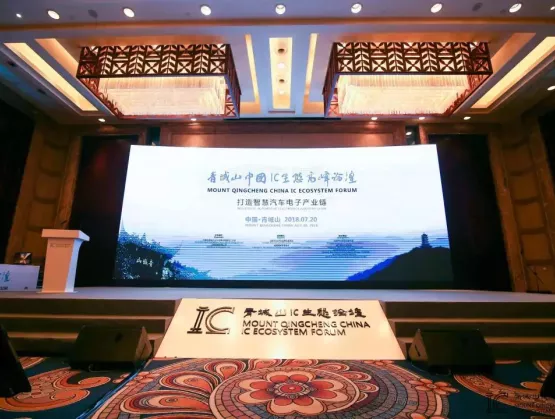
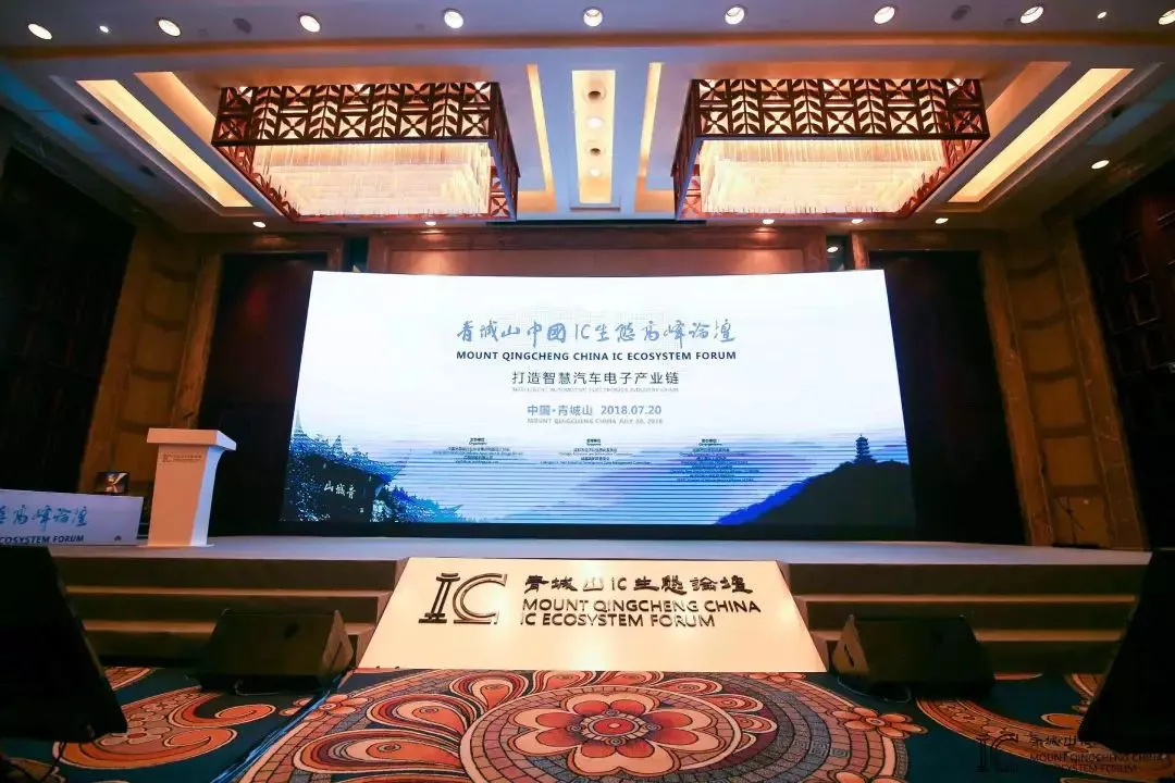
FD-SOI was a very important topic during the recent Mount Qingcheng China IC Ecosystem Forum. To situate things, Mount Qingcheng, with its lush hills and waterways, is located just outside of Chengdu. That of course is where GlobalFoundries is building its new fab, which will be the first in China to run FD-SOI. Chengdu is also a key city in China's automotive electronics landscape. [caption id="attachment_12236" align="alignright" width="300"] (Image Courtesy: VeriSilicon)[/caption] The theme of the forum was Building a Smart Automotive Electronics Industry Chain. Over 260 decision-makers from government, academia and industry attended – and the SOI Consortium had a significant presence. The event was chaired by Wayne Dai, CEO/Founder of consortium member VeriSilicon, and tireless champion of the the FD-SOI ecosystem in China and worldwide. Morning keynotes were given by: Carlos Mazure, Soitec CTO and SOI Consortium Executive Co-Director; Mark Granger, GF's VP of Automotive Product Line Management; and Tony King-Smith, Executive Advisor at AImotive, a GF 22FDX customer. BTW, transcripts of all the talks are available through Gasgoo, China's largest automotive B2B marketplace. You can click here to access them. (They're in Chinese – but you can open them in the language of your choice using the major translation websites.) Chengdu Officials Affirm Support for FD-SOI Fan Yi, Deputy Mayor of Chengdu, spoke extensively of FD-SOI in his keynote on the importance of rapidly developing smart cars. He heralded the “spectacular” new GlobalFoundries fab there. Following a meeting with the company's top brass the day before, he affirmed GF's confidence in their investment. There is a solid roadmap for FD-SOI, he noted, and efforts are underway to accelerate the move into production and expand education and training. He cited the benefits of FD-SOI for the entire supply chain, from design through package and test, raising the level of the entire IC industry to new heights. The government, he said, attaches great importance to this enterprise. Their thinking regarding intelligent transport in China is integrated with the overall approach to smart cities. 
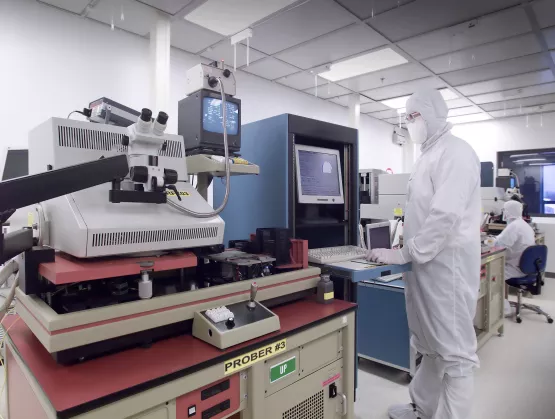
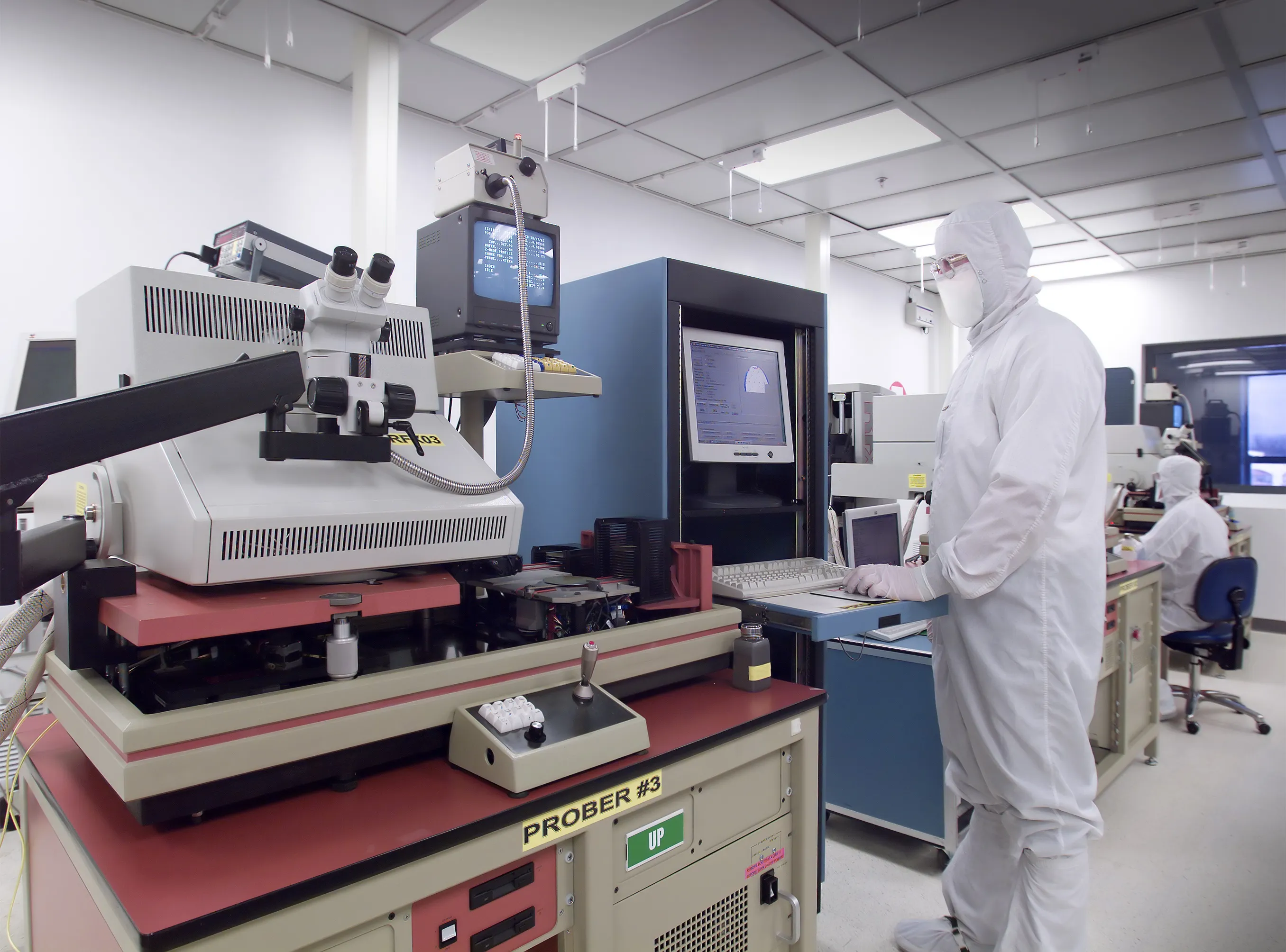
SOI Consortium Leads Industry Keynotes [caption id="attachment_12232" align="alignleft" width="300"] Wayne Dai, VeriSilicon Founder and CEO (Photo courtesy VeriSilicon)[/caption] In his opening remarks, Wayne Dai emphasized the need for China to seize the advantage in the next round of development opportunities in the automotive electronics industry. This year's Qingcheng forum, he noted, brought together key representatives from across the supply chain, from of the highest to the deepest reaches of the smart car electronics industry, and across markets, technologies, solutions, industrial ecosystem, standards and regulations. In his talk on how FD-SOI is boosting the accelerated development of automotive electronics, Carlos Mazure presented the SOI Industry Consortium. He noted that the Consortium promotes mutual understanding and development across the ecosystem. SOI is already present throughout automotive applications, he noted. There are currently about 100mm2 of SOI per car, in such diverse areas power systems, transmissions, entertainment, in-vehicle networking and more. SOI will experience especially high growth in electrification, information/entertainment, networking, 5G, AI/edge computing and ADAS. He then went on to give some history and an extensive overview of the major trends and highlights we've seen over recent years. He finished by giving examples of convergence across the supply chain with IC manufacturers working with automakers to lower power, increase processor performance and advance 5G. [caption id="attachment_12233" align="alignright" width="665"] Carlos Mazure, Soitec CTO and SOI Consortium Executive Co-Director; Tony King-Smith, Executive Advisor at AImotive and Mark Granger, GF's VP of Automotive Product Line Management (Photo courtesy VeriSilicon)[/caption] GF's Mark Granger addressed the rapid development of automotive electronics. In certain areas, he said, he sees growth rates of over 20%. They are working on building the Chengdu ecosystem, especially for design, and in cooperation with the rest of the supply chain. Furthermore, he reminded the audience, when you talk about cars, travel implies that you also talk about IoT as well as things like infotainment and integrated radar ICs. In addition to cost and power efficiencies, the AEC-Q100 standard for IC reliability in automotive applications is also pushing designers to turn to FD-SOI. In the GF meeting with Chengdu government officials (referenced above in deputy mayor Fan Yi's talk), he too confirmed their support of FD-SOI as a key technology for China. GF is currently cooperating with about 75 automotive partners, he said, and the company is looking to increase cooperation with partners in the Chengdu region. Tony King-Smith talked about the 22FDX test chip AImotive is doing with Verisilicon and GF. In case you missed it, in June 2017 AImotive announced its AI-optimized hardware IP was available to global chip manufacturers for license. AiWare is built from the ground up for running neural networks, and the company says it is up to 20 times more power efficient than other leading AI acceleration hardware solutions on the market. In the same announcement, they revealed that VeriSilicon would be the first to integrate aiWare into a chip design,and that aiWare-based test chips would be fabricated on GF's 22FDX. The chip is expected to debut this year. While the afternoon agenda was not specific to FD-SOI, it did focus on the "smart cockpit" and "intelligent driving", with talks by nine leading players in China's automotive IC and investment communities. ~ ~ ~Note: Many thanks to the folks at VeriSilicon, who wrote up this event for their WeChat feed, and shared photos with us here at ASN.
Read More
SEMI has launched a mentoring program that pairs seasoned industry professionals with university students and professionals wanting to advance their careers. The program is designed to help tackle the semiconductor industry’s workforce shortfall and prepare the next generation of innovators. Under the program, SEMI members with years of professional experience share their knowledge with developing talent and help build their professional networks as they embark on their careers in the microelectronics industry.As the microelectronics manufacturing industry faces increasing challenges in recruiting, training and retaining a diverse pool of highly skilled talent to sustain the remarkable pace of innovation globally, SEMI has made workforce development a top strategic priority. Globally, the industry is confronted with more than 10,000 job vacancies.To help build the workforce of the future, SEMI has rolled out industry-wide programs to address a chief reason for the workforce shortage – increasing competition from other technology sectors. The initiatives include enhancing industry awareness of the industry’s critical need for talent, increasing the representation of women, and supporting young professionals and university students soon to be making important career decisions. The new SEMI Mentoring Program builds on those initiatives by guiding the next generation of innovators.With mentoring a proven method to develop talent, SEMI has contracted with Chronus – an experienced provider of a software mentoring platform tailored to support the SEMI Mentoring Program.SEMI Mentoring Program: Roles and Responsibilities This is a formal relationship in which mentors guide mentees in their professional development. The mentor will answer questions and take a personal interest in, guide, encourage, and support the mentee. The mentor will meeting monthly with the mentee and follow up as needed. The mentee will set up the first meeting to discuss professional goals, topics he or she would like to cover and timing for subsequent. Both mentor and mentee will commit to remain connected for at least six months. Frequently Asked Questions Q: How are meetings conducted?A: Mentors and mentees can meet face-to-face or virtually, but should meet for a minimum of one hour once a month for six months.Q: How are goals set?A: The mentor and the mentee agree on goals during their first meeting. The mentee is responsible for arranging meetings, preparing the agendas, and any other pre-meeting work. This will ensure that the discussions touch on the topics that matter most to the mentees.Q: What happens once the six months are up?A: You can continue an unofficial relationship if both parties agree, or you can search for a new mentor or mentee by reapplying through your mentor profile.Q: What is SEMI’s role?A: SEMI is here to help match you based off your preferences, facilitate the relationship, provide materials to guide your experience, and help resolve any program or platform related issues.Q: What are the program eligibility requirements for mentors?A: A mentor must be an employee of a SEMI member organization with a minimum of five years’ professional experience to mentor a university student, or seven years’ professional experience to mentor a developing professional.Q: What are program eligibility requirements for mentees?A: Developing Professional Program Developing professional, 0-7 years in their career Employed by a SEMI member organization University Program At minimum, a rising junior enrolled in a university program (students through PhD level accepted) Completing a STEM major Within 6 months of graduation if currently out of school and seeking employment Preferred: Interest in the microelectronics industry Q: Why be a mentee?A: Learn from an experienced industry professional and accelerate your professional development.Q: Why be a mentor?A: Being a mentor will allow you to grow as a leader while giving you the rewarding experience of guiding someone’s growth path firsthand. Join us in shaping the future of our industry by becoming a mentor or mentee. Sign up here! For more information about the program, please contact Cristina Sandoval, manager of Workforce Development, at [email protected].
Read More
2Q’18 Electronic Supply Chain Growth Update Chart 1 is a preliminary estimate of global growth of the electronic supply chain by sector for 2Q’18 vs 2Q’17. Note the strong performance of semiconductors, SEMI capital equipment and passive components. Chart 2 gives preliminary 2Q’18 world electronic equipment growth by type. Global electronic equipment sales rose an estimated 9%+ when consolidated into US dollars in the second quarter of this year compared to the same quarter in 2017. Based on this, data global electronic equipment sales growth appears to have now peaked on a 3/12 growth basis for this present business cycle (Chart 3). As a caution these charts are based on a combination of actual company financial reports and estimates for companies that have not yet reported their calendar second quarter financial results. A number of large companies have yet to report but these early estimates have historically been close to final growth values. We will update Chart 1 next month.Semiconductor Capital Equipment Business Cycle Semiconductor capital equipment sales are historically very volatile, with their growth fluctuating MUCH MORE than electronic equipment (Chart 4). However, both series appear to have peaked on a 3/12 basis for this current cycle. Semiconductors, SEMI capital equipment and Taiwan chip foundry sales all are seeing slower growth. 3/12 values 1 still indicate an expansion but slower growth is indicated. Supply chain performance in the second half of this year bears careful watching!Walt Custer of Custer Consulting Group is an analyst focused on the global electronics industry.
Read More
IntroductionStarting July 4, 2022, PFOA (Perfluorooctanoic acid) levels in semiconductor manufacturing and related equipment (SMRE), including replacement parts, entering the European Union (EU) will be restricted to 25 ppb per component (or any part thereof). Semiconductor equipment components (and the parts thereof) of particular concern include fluid tubing and fittings, pipe/seal tape, wire and cable insulation, filters, valves, tanks, panels, reaction vessels and o-rings; if they are made from fluoropolymers or fluoroelastomers.When PFOA is used as an aid to the manufacture fluoropolymers such as PTFE, PFA, PVDF or fluoroelastomers such as FKM and FFKM (collectively referred to as fluoromaterials), an unintended PFOA residue can be trapped within the fluoromaterial. Buyers of components used in SMRE are usually unaware of the processing method used for any fluoromaterials they may contain, and, as a consequence, the potential for PFOA residue. This lack of information about potential PFOA residues could result in regulatory enforcement actions and restricted market access, particularly in the EU.The impact of restrictions on fluoromaterials used in SMRE has been introduced in previous SEMI articles ‘Fluorinated Compound Restrictions May Trigger Costly Equipment Changes’ and ‘Fluorinated Substance Restrictions Triggers Costly Equipment Changes.’PFOA and its related compounds, such as the ammonium salt APFO (collectively called PFOA in this article), are recognized internationally as hazardous chemicals and are now targeted for regulatory restriction in the U.S., Taiwan, Canada and the EU. The UN Stockholm Convention on Persistent Organic Pollutants (POPs) is also considering listing PFOA, which could lead to additional international restrictions.The SEMI EHS Division PFOA Compliance Working Group has been working to understand: The likelihood of PFOA residue entering the supply chain of new components The residual level of PFOA in fluoromaterials produced prior to the phase out of PFOA by some manufacturers The impact of PFOA residue on the secondary equipment market This SEMI resource page, ‘Elimination of PFOA from the Equipment Supply Chain,’ and the supporting FAQ contain the Working Group’s key findings and conclusions.PFOA in the Fluoromaterial Supply ChainSignatories to the U.S. EPA Stewardship Program, which include FluoroCouncil members, eliminated PFOA from their manufacturing processes by 2013. However, other fluoromaterial manufactures – particularly in China, Russia and India – might still use PFOA and pose a significant risk to the worldwide supply chain.China, the world’s largest fluoromaterial producer, accounts for 53 percent of global production of PTFE and 38 percent of worldwide production of PVDF, FEP and FKM. An estimated 75 percent to 85 percent of fluoromaterials are manufactured using PFOA in China. Fully 25 percent of these fluoromaterials are exported, primarily to the U.S, Japan, EU and India. What’s more, finished goods made from or containing fluoromaterials that might be used as components in SMRE are exported from China.Documentation that traces fluoromaterials through the supply chain back to the original fluoromaterial manufacturer is key to meeting the PFOA regulatory requirements. This traceability can be straightforward in cases when an SMRE manufacturer directly specifies the use of a fluoromaterial in a custom-fabricated fluoromaterial component. However, for off-the-shelf components (e.g., cable ties, wiring insulation, tubing) or the components assembled from these components (e.g., controllers), the complexity and dynamics of the supply chain makes traceability back to the original fluoromaterial producer almost impossible.Residual PFOA Levels If, or how much, PFOA/APFO residue is contained in a fluoromaterial depends on the manufacturing process. Details of the manufacturing processes are proprietary and vary widely. Post manufacturing thermal treatments, such as sintering, extrusion, and molding, can result in the rapid thermal decomposition of APFO above 250C, but PFOA is significantly more stable. The temperature and time of thermal treatments is also proprietary and varies depending on the type of fluoromaterial and what is being made.This variability makes it impossible to estimate the likely level of trapped PFOA or APFO in a finished component or a part thereof. It is unwise to use data on the level of residue made known for one case to extrapolate the level of residue across the fluoromaterial industry. However, an industry-wide range on the order of 1ppm-10ppm (nearly 1000 times the EU limit) is suspected. Testing for the presence of PFOA/APFO at 25ppb in components is also problematic as there is no standard test method, and results among the custom methods developed in each test lab may vary.Given this uncertainty in test methods, a system of supplier declarations warrants consideration.Impact on Secondary (Used) EquipmentThe EU REACH restrictions apply to SMRE and replacement parts placed on the market at any time (not just initial placement – known as “first placing on the market”). For fluoromaterial components manufactured prior to 2013, there is a higher likelihood of residual PFOA/APFO levels exceeding the 25ppb limit of EU REACH. In principle all the SMRE components containing fluoromaterials should be investigated, and those containing PFOA above 25ppb must be replaced before the SMRE can be legally placed again on the EU market. Companies (e.g., semiconductor manufacturers) in the EU who wish to sell used equipment within the EU will be required to demonstrate the used equipment is in compliance. Selling older used equipment would likely be unprofitable after necessary investigations and component replacements are completed.Next StepsWhile the EU semiconductor manufacturing industry heavily depends on the secondary (used) equipment market, EU regulators may be unaware of the PFOA restriction’s damaging impact to this market. The EHS Division PFOA Working Group, in conjunction with SEMI Europe, is now considering how to bring this concern to the attention of regulators and to collaborate and lobby for effective changes including possible modifications to the EU Persistent Organic Pollutants (POPs) regulation.
Read More
U.S.-China Trade War Heats UpThe U.S. Trade Representative (USTR) yesterday released a 25 percent tariff on $16 billion in imports from China, including 29 tariff lines that represent the heart of the semiconductor industry. These tariff lines include semiconductor products such as machines and spare parts used to make, wafers, flat panel displays, masks and chips, and will cost SEMI’s 400 U.S. members an estimated more than $500 million annually in additional duties.SEMI, along with hundreds of companies, including Lam Research and KLA-Tencor, submitted written comments, requesting the removal of tariff lines from the proposed list. SEMI also testified on behalf of the semiconductor industry, joining more than 80 other companies, including Applied Materials, in opposing the duties before an U.S. government interagency panel in late July.This trade action is on top of the already imposed $34 billion U.S. tariff list, which will cost SEMI’s U.S. members tens of millions of dollars annually. In the coming days, USTR will publish details on how U.S. companies can request the exclusion of products from the $16 billion tariff list, much as it did for the first round of $34 billion.In a swift retaliation, China announced a 25 percent tariff on $16 billion in U.S. exports, including products vital to semiconductor manufacturing such as chemicals, test equipment and other parts. Both U.S. and China tariffs will take effect on August 23.The new tariffs come as China considers tariffs on $60 billion of U.S. imports, and the U.S. weighs additional duties on $200 billion of Chinese imports – a wave that would inflict even deeper damage on the U.S. semiconductor industry. This latest round of U.S. tariffs would cover goods used in microelectronics manufacturing, including chemicals, glass products and spare parts. SEMI will testify against the $200 billion tariff list later this month. If your company expects to be impacted by the proposed tariffs on $200 billion worth of goods, please contact SEMI staff.SEMI stands firm in its belief that none of the tariffs address U.S. concerns over China’s trade practices. Instead, they harm companies in the semiconductor supply chain by increasing business costs, introducing uncertainty and stifling innovation. SEMI will continue to engage with policymakers as both the U.S. and China $16 billion tariff lists are implemented. We will also be evaluating the products covered by the $200 billion U.S. list and the $60 billion Chinese list as both are further considered. We encourage members to review these lists to determine impact on their companies. For more information, please contact Jay Chittooran, Public Policy Manager at SEMI, at [email protected].
Read More
Did you miss the SEMI International Standards Reception at SEMICON West 2018? Not to worry, here are the highlights.SEMI honored two Standards industry leaders for their outstanding accomplishments in developing Standards for the electronics and related industries.Two awards were given recognizing the efforts of each member. The Technical Editor Award recognizes the efforts of a member to ensure the technical excellence of a committee’s Standards. This year’s recipient is Sean Larsen of Lam Research. Mr. Larsen has led the North America EHS Committee and multiple EHS task forces for over a decade. His knowledge of the Regulations, Procedure Manual, and Style Manual, combined with his vast experience in the industry, ensures that complex safety matters are explained in a clear, consistent manner, and ballot authors frequently rely on him for his technical skills in preparing ballots.In addition to co-chairing the North America EHS Committee, Mr. Larsen is currently the co-leader of the SEMI S22 (Electrical Design) Revision TF, the SEMI S2 Non-Ionizing Radiation TF, the SEMI S2 Korean High Pressure Gas Safety TF, and the Control of Hazardous Energy TF.The Corporate Device Member Award recognizes the participation of the user community and is presented to individuals from device manufacturers. This year’s recipient is Don Hadder of Intel. Mr. Hadder has been actively involved in the Standards Program for several years, and currently leads the Chemical Analytical Methods Task Force and chairs the North America Liquid Chemicals Committee. He has successfully re-energized the committee, which is now focused on enabling continued process control improvements for advanced nodes. He recently drove the development of a critical new standard: SEMI C96, Test Method for Determining Density of Chemical Mechanical Polish Slurries, the first document in a series of SEMI Standards that will be devoted specifically to CMP slurry users, IDMs, slurry suppliers, metrology manufacturers and OEM equipment suppliers.Mr. Hadder has worked at Intel for 23 years, where his experience and system ownership has been in Diffusion, Wet Etch, Planar-CMP, Ultra-Pure Water, Waste Treatment Systems, Abatement and Vacuum Systems, Bulk and Specialty Gas, Bulk Chemical Delivery and Planar Chemical Delivery.James Amano, Sr. Dr. International Standards, opened the reception with a few words. He noted that the total number of published SEMI Standards is nearing 1000, and that these documents serve as the backbone of modern day semiconductor manufacturing. SEMI president and CEO Ajit Manocha, speaking at the SEMI International Standards Reception at SEMICON West. Ajit Manocha, President and CEO of SEMI, reminisced how he was an active Standards Member, and how much he got out of SEMI Standards as a young engineer at Bell Labs. He passionately emphasized that SEMI Standards remain critical in this era of new materials and disruptive architectures and processes, calling them the "oxygen of the industry."Laura Nguyen is coordinator, International Standards, at SEMI.
Read More