downloadGroupGroupnoun_press release_995423_000000 copyGroupnoun_Feed_96767_000000Group 19noun_pictures_1817522_000000Member company iconResource item iconStore item iconGroup 19Group 19noun_Photo_2085192_000000 Copynoun_presentation_2096081_000000Group 19Group Copy 7noun_webinar_692730_000000Path
Skip to main content
Default Banner Image

France

Date: May 8, 2026

Location: Drammen, Norway

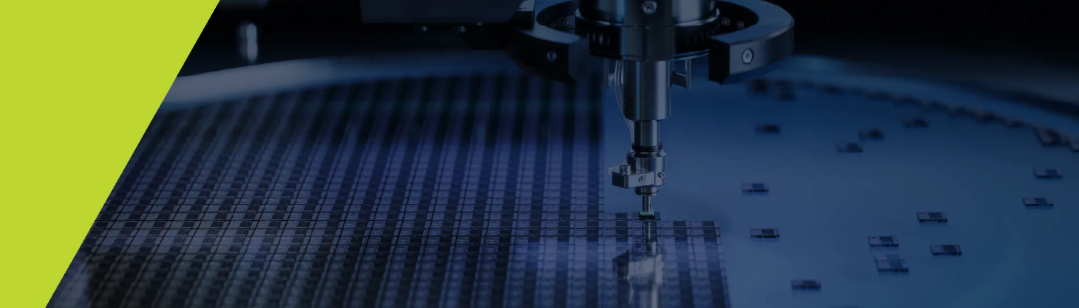
Board-level and semiconductor test data are often analyzed separately, limiting correlation across the product lifecycle. Linking PCB assembly (PCBA) test results, including in-circuit and functional test, with upstream wafer, sort, and final test data remains difficult, particularly in photonics, advanced packaging, and high-density integration environments. yieldWerx and WATS announce a partnership to bridge this gap in the PCB test and semiconductor manufacturing workflows.

WATS is a test data management platform purpose-built for electronics manufacturers. It captures, standardizes, and analyzes high-volume test data from PCBA (printed circuit board assembly) production environments, including in-circuit test (ICT), functional test, and final test, giving engineers real-time visibility into board-level yield, anomalies, and quality metrics across the production line.

yieldWerx operates at the semiconductor level, connecting data across wafer fabrication, wafer sort, die, and packaged device test. Its enterprise analytics platform enables advanced yield analysis, traceability, and root cause investigation from design through silicon manufacturing.

Together, the platforms address the full product stack. This allows manufacturers to correlate PCBA-level signals with silicon quality data, improving visibility across test stages and enabling more effective analysis of yield and reliability issues.

Customer and industry benefits include:

Real-time PCBA test visibility for faster identification of yield and quality issues

Improved correlation between board-level test results and upstream chip or wafer data

Reduced time spent reconciling data across disconnected systems

Earlier detection of cross-stage patterns impacting yield and reliability

Faster root cause analysis spanning silicon, assembly, and board-level test

Better alignment between electronics manufacturing and semiconductor supply chain

The combined solution supports open architectures, APIs, and flexible deployment models, enabling integration without large-scale system changes.

About yieldWerx

yieldWerx is an enterprise analytics platform connecting data across the semiconductor product lifecycle, from design and wafer fabrication through wafer sort, die, and packaged device test, enabling advanced yield analysis, traceability, and data-driven decision-making across cloud, on-premises, and hybrid environments.

About WATS

WATS is a test data management and analytics platform developed by Virinco, built to collect, standardize, and analyze data from electronics manufacturing test systems. It provides real-time visibility into board-level performance across ICT, functional test, and final test operations, helping engineers monitor yield, detect anomalies, and improve quality at high volume.

Statements from Leadership
"We are excited to partner with yieldWerx. Our customers manufacture complex electronics where board-level test data alone only tells part of the story. By connecting PCBA production test data with yieldWerx's upstream semiconductor intelligence, we can give them a more complete picture of their product quality and yield." -- Tom Lomsdalen, CEO, Wats

“Our customers have been asking for a unified view that links semiconductor yield data with downstream electronics test results, and this partnership delivers exactly that. Together, yieldWerx and WATS empower engineering teams to move faster on root cause analysis, reduce escapes, and make smarter decisions across the entire product lifecycle.” -- Aftkhar Aslam, CEO, yieldWerx

For further information, please visit https://www.yieldWerx.com or https://www.Wats.com/.

Semiconductor industry leader takes the helm to accelerate Beneq’s next phase of growth in atomic layer deposition

Espoo, Finland, 8 May, 2026 – Beneq Oy, the home of atomic layer deposition (ALD), today announced the appointment of Dr. Jason Harrison as Chief Executive Officer. Dr. Harrison succeeds Dr. Tommi Vainio and will lead Beneq into its next phase of growth across semiconductor, optical, and emerging technology markets.

A Strategic Leadership Transition
Beneq enters its next phase of growth from a position of strong commercial momentum. Recent milestones include the qualification of the Beneq Transform® cluster tool for volume production of GaN power and RF filter devices; the introduction of Beneq Transmute™ and Beneq Transform® XP, both engineered for high-volume manufacturing (HVM) of specialty semiconductors; growing adoption of the P-Series for coating critical chamber parts in advanced node devices; and selection of the C2R™ for AR waveguide production in next-generation XR optics.

Against this backdrop, the Board of Directors has determined that the time is right to align executive leadership with the company's evolving strategic priorities. As part of this transition, Dr. Tommi Vainio has decided to step down as CEO to pursue other opportunities. The Board of Directors extends its sincere thanks to Tommi, whose leadership advanced Beneq's technology platform, strengthened its market position in thin film deposition, and guided the company through important stages of its development.

A Proven Leader for a Scaling ALD Business
Dr. Harrison brings extensive global experience across the semiconductor and advanced technology sectors. He holds a Ph.D. in Quantum Chemistry and has built a distinguished career spanning device manufacturing, process development, and equipment solutions, with senior leadership roles at Intel, Lam Research, Veeco, and Applied Materials covering research and development, new product introduction, global account management, and business unit leadership. This combination of technical depth and commercial acumen positions him to scale Beneq’s commercial execution and growth across its global customer base.

Looking Ahead
Under Jason’s leadership, Beneq will accelerate strategic execution across its expanding portfolio, deepen customer engagement across North America, Asia, and Europe, and continue investing in innovative ALD solutions from R&D to HVM to deliver long-term value to customers, employees, and stakeholders.

Dr. Patrick Rabinzohn, Member of the Board of Directors, Beneq, said: “Jason brings the technical depth, the business and account management experience, and the global perspective Beneq needs at this stage of its growth. His academic background and compelling track record across the semiconductor industry positions Jason to build on the momentum the company generated especially.”

Dr. Jason Harrison, Chief Executive Officer, Beneq, added: “Beneq has a strong technology foundation, a talented team, and a growing pipeline of customers in some of the most important markets in semiconductors and optics. I look forward to working with the team to accelerate execution and deliver on the trust our customers place in us.”

About Beneq
Beneq pioneered industrial production of Atomic Layer Deposition (ALD) with the introduction of the first commercial ALD equipment in 1984. Today, Beneq advances ALD adoption and validation with a portfolio that includes the Beneq Transform®, Transform XP, Transform 300, and Transmute™ for specialty semiconductor device fabrication; TFS 200 and TFS 500 for R&D; the P400A, P800, and P1500 batch systems for coating critical semiconductor chamber components and complex part geometries; and spatial ALD platforms such as the C2R™ and roll-to-roll processing equipment. Headquartered in Espoo, Finland, Beneq enables ALD integration from lab to fab for semiconductors, optics, and functional coatings.

Press Contacts
Lie Luo
Head of Marketing
[email protected]

ROSENHEIM, Germany / KUALA LUMPUR, 5 May 2026 — esmo group (esmo), a leading global full-service systems integrator, developer, and supplier of advanced automation solutions for the semiconductor test industry, today announces the debut of its X-change Cart. A dedicated, semi-automated Device Interface Board (DIB) exchange system that enables a complete load board changeover by a single operator in under one minute, the X-change Cart addresses the safety, efficiency, and reliability challenges associated with manual board handling on the semiconductor test floor.

In high-mix semiconductor test environments, load board changeovers are a frequent and operationally significant activity. The reliance on manual handling has long presented challenges around changeover time, operator safety, and the risk of damage to high-value boards.

“Across test floors, we kept seeing the same pattern,” said Josef Weinberger, Head of Business Unit, esmo semicon. “Board changeovers were slow, physically demanding, and too dependent on individual technique. In tight spaces, that's where mistakes happen and time is lost. That observation drove us to build a dedicated solution that makes changeovers fast, repeatable, and manageable by a single operator in under a minute.”

Engineered for the Modern Test Floor

The X-change Cart removes the physical demands and variability of manual board handling from the equation entirely. Through a structured, HMI-controlled process, a single operator can lock, rotate, and transfer a board to the tester within a minute. The ability to carry two boards in a single trip makes that timescale achievable in practice. Thoughtful design details, including a ±180° rotation at the locking mechanism and a ±90° tower swivel, address the real-world constraints of a busy test floor.

Broad compatibility with leading ATE platforms (e.g. Teradyne, Advantest, SPEA and more) facilitates integration into existing multi-vendor environments without reconfiguration, allowing OSATs and IDMs to realise multiple benefits without disruption to their current setup.

For facilities with longer-term automation objectives, an optional configuration allows the interface tower to be mounted onto a customized AGV or AMR, providing a practical upgrade path toward autonomous test floor operations. The modular design further allows additional features to be incorporated as operational requirements evolve.

Weinberger added, “Reliability in production comes down to the details. The gripper head is engineered to perform consistently under real production conditions, with ESD-safe construction ensuring the board is protected at every point of contact. That level of engineering discipline is what makes the difference on a real production floor.”

X-change Cart Key Features

  • Modular DIB exchange system for reliable, error-free board loading and unloading
  • One-person operation — complete board change in under one minute
  • Transports two load boards simultaneously for rapid exchange
  • Full multi-axis rotation: ±180° at locking mechanism | ±180° Y-axis | ±90° Z-axis
  • Compatible with leading ATE platforms — Teradyne, Advantest, SPEA and more
  • Interfaces with test head, prober, DIB-loader, storage rack, and maintenance workbench
  • Tower swivels ±90° for use in narrow corridors and constrained test floor layouts
  • Integrated Human-Machine Interface (HMI), sensor detection, safety hand-brake, and modular battery
  • Optional: fully automated configuration mountable on AGV or AMR

The X-change Cart will be available for live demonstration at the esmo booth throughout SEMICON Southeast Asia 2026. Visit esmo at Booth 2145, Hall 8, Level 2, MITEC Kuala Lumpur from 5–7 May 2026, or contact [email protected] to arrange a meeting or request further information.

Brewer Science Earns 2026 USA TODAY Top Workplaces Award
Employee-Owner Feedback Recognizes Company’s People-First Culture

Rolla, MO – April 14, 2026 – Brewer Science, Inc., a global leader in developing and manufacturing next-generation materials and processes for the microelectronics and optoelectronics industries, has been named a 2026 USA TODAY Top Workplace. The recognition underscores Brewer Science’s long-standing commitment to fostering a people-first culture.

The USA TODAY Top Workplaces award honors organizations with 150 or more employees that have created exceptional workplace cultures centered on trust, engagement, and employee well-being. This year, more than 42,000 organizations were invited to participate. Award recipients are recognized for building environments that prioritize employee listening and meaningful engagement. USA TODAY showcased the winners online and at the National Awards Summit in Las Vegas.

Winners are determined solely by authentic employee feedback collected through a confidential survey administered by Energage, the HR research and technology company behind the Top Workplaces program since 2006. Results are based on employee responses to Workplace Experience Themes, which research shows are strong indicators of organizational health and performance.

“Earning a USA TODAY Top Workplaces award is a testament to an organization’s credibility and commitment to a people-first culture,” said Eric Rubino, CEO of Energage. “This award, driven by real employee feedback, is more than just a recognition — it’s proof that your employees believe in the organization and its leadership. Job seekers and customers look for this trusted badge of credibility and excellence. It signals a company that values its people, and that kind of culture resonates in today’s competitive market.”

In addition to the national USA TODAY recognition, Brewer Science continues to receive strong regional and industry-specific honors. In 2025, the company was named a Top Workplace in Greater St. Louis for the ninth consecutive year and earned recognition as a 2025 National Top Workplace in the Manufacturing Industry. These sustained accolades reflect a culture intentionally designed to provide employee-owners with a fulfilling and purpose-driven work experience that fuels innovation across the microelectronics industry.

“Delivering customized solutions to customers’ complex challenges requires a strong sense of clarity and commitment across the company,” said Dan Brewer, co-CEO of Brewer Science. “That commitment is rooted in our value to create an environment where employees are empowered to think creatively, collaborate openly, and innovate boldly. Our employee-owners take pride in the products they bring to our customers, partners, and the industry as a whole.”

Learn more about Brewer Science’s culture and explore career opportunities at:
https://www.brewerscience.com/about-us/company/careers/

ABOUT BREWER SCIENCE
Brewer Science is a global leader in developing and manufacturing next-generation materials and processes that foster the technology needed for tomorrow. Since 1981, we’ve expanded our technology portfolio within advanced lithography, advanced packaging, smart devices, and printed electronics to enable cutting-edge microdevices and unique quality monitoring systems for water and air applications. We are Certified Employee-Owned and a Certified B Corporation™, using our business as a force for good. Our headquarters are in Rolla, Missouri, with customer support throughout the world. Learn more at: www.brewerscience.com.

###

Company Contact:
Nathan Ayres
Email: [email protected]

ABOUT ENERGAGE
Energage is a purpose-driven company that helps organizations turn employee feedback into useful business intelligence and credible employer recognition through Top Workplaces. Built on 20 years of culture research and the results from 30 million employees surveyed across more than 80,000 organizations, Energage delivers the most accurate competitive benchmark available. With access to a unique combination of patented analytic tools and expert guidance, Energage customers lead the competition with an engaged workforce and an opportunity to gain recognition for their people-first approach to culture. For more information or to nominate your organization, visit energage.com or topworkplaces.com.

Belgium France Germany Ireland Italy United States Adv_Packaging Training Featured Speakers

Course Description 

This course will stress the impace of the IC and End product requirements, i.e., smaller, better, cheaper" and their influence on the manufacturing processes. Topics include area packaging - ball grid arrays, flip chip, fanout, attaching dies and chip scale packages, and the assembly technologies - chip & wire, tape automated bonding, and flip chip, as well as emerging technologies, namely, 3-D and stacked die, and packaging reliability issues.

Who Should Attend

This course is intended for both manufacturing and R&D know-how in IC packaging professionals, including but not limited to:

  • Engineers
  • Managers
  • Process Engineers
  • R&D Engineers
  • Sales and Application Engineers who supply packaging materials and tools

Learning Objectives

  • Identify the wide variety of package types and how they align with different application uses.
  • Understand chip interconnection technologies (such as wirebond, flip chip, or thin film) and chip encapsulation
  • Identify the materials and processes used in packaging.
  • Summarize the current state of the art packages, such as chiplets and heterogeneous packaging.
  • Gain a foundational understanding of what packaging is and its importance to the microelectronics industry. 


Important Information

Note that only the person who registered will receive a certificate of completion. This virtual training will not be recorded. Attendees must be present to access the course knowledge. 

Can't find the training link on the day of? After you register, you will receive the link to the live training via the email address you provided. In addition, you will receive email reminders about 24 hours in advance and an hour before with the same link. Please keep these emails on hand to access the training on time. If you do not see any confirmation emails, please check your junk/spam folders before contacting SEMI U for support.

United States

Dr. Terry Alford
Dr. Terry Alford
PT International
- SEMI U

Strengthen your knowledge and skills by learning about IC packaging, assembly, and package/substrate and Heterogeneous Integration & Chiplets. 

Pricing

             Early Bird Pricing $100 off

  • Members: $845   $745
  • Non-Members: $945  $845

* * Group pricing for 20+ attendees: $9900
Any questions, please contact [email protected]

7:30 am - 11:30 am Off Add to Calendar Disabled America/Los_Angeles Register Now
Event format
Promote in calendar
Off
Belgium France Germany Ireland Italy United States Wafer Training

Course Description 

This course provides a comprehensive introduction to semiconductor manufacturing, guiding participants through the complete journey from silicon fundamentals to chip fabrication and packaging. Designed for professionals new to the semiconductor industry, the course explains key concepts, terminology, devices, and manufacturing processes used in modern fabs. 

This course is divided into four modules, enabling a progressive learning experience that builds from fundamentals to manufacturing execution. Participants will gain a clear understanding of how chips are made, the role of transistors, and the steps involved in front-end manufacturing, followed by back-end assembly and packaging processes. The course also introduces the broader semiconductor ecosystem, including supply chain players, helping learners connect technical fundamentals with real-world manufacturing practices. 

Who Should Attend

This course is designed for sales and marketing professionals, as well as new employees, students, and anyone interested in gaining a knowledge about semiconductor manufacturing.   

Learning Objectives

Upon completion of the course, participants should be able to:

  • Explain fundamental semiconductor concepts, including silicon materials, doping, PN junctions, and basic device behavior. 
  • Identify and correctly use common semiconductor manufacturing terminology.
  • Outline the key steps involved in front-end wafer fabrication, from bare silicon to patterned wafers.
  • Summarize back-end manufacturing processes, including assembly, packaging, and testing.

Topics Included

  • Module 1: Semiconductor Fundamentals

    Introduces semiconductor basics, silicon materials, doping PN junctions, and core device concepts, building a foundation for understanding how electronic devices function.

  • Module 2: Semiconductor Terminologies and Manufacturing Context

    Covers essential semiconductor terminology, cleanroom concepts, supply chain players, process nodes, and packaging to help learners navigate manufacturing discussions with confidence.

  • Module 3: Front-end and Back-end Semiconductor Manufacturing

    Provides an overview of the key steps involved in front-end wafer fabrication and back-end assembly, packaging, and testing processes.

  • Module 4: Transistors and Their Operation

    Explains different types of transistors and their working principles, showing how transistors function as switches and amplifiers inside integrated circuits. 

Important Information

Note that only the person who registered will receive a certificate of completion. This virtual training will not be recorded. Attendees must be present to access the course knowledge. 

Can't find the training link on the day of the training? After you register, you will receive the link to the live training via the email address you provided. In addition, you will receive email reminders 24 hours in advance and 1 hour before, with the same link. Please keep these emails on hand to access the training on time. If you do not see any confirmation emails, please check your junk/spam folders before contacting SEMI U for support.


Mayura Padmanabhan
Program Manager
SEMI


United States

SEMI U

Strengthen your knowledge and skills by learning about the journey from silicon fundamentals to chip fabrication and packaging. 

Pricing                     
  • Members:  $149
  • Non-Members:  $179

* * Group pricing for 10+ attendees: $1,299 and 20+ attendees: $2,399
Any questions, please contact [email protected]

8:00 am - 12:00 pm Off Add to Calendar Disabled America/Los_Angeles Register Now
Event format
Promote in calendar
Off
Belgium China France Germany India Ireland Italy Japan Malaysia Singapore South Korea Taiwan United States Vietnam Water Mgmt banner 350x317 Business Executive Technical

Thank you to our sponsors:  


         Sundt Construction Company & General Contractor | Sundt                                   SCREEN logo


Highlighted content

United States

9:00 am - 9:10 am

Welcome and Overview of the Water Management Working Group

9:10 am - 9:25 am
Pascal Osten
Leader, Water Solution Providers Cohort
Pascal Osten
DAS Environmental Expert GmbH

Procedures Guide

9:25 am - 9:35 am
Catherine Marsan-Loyer
Co-Lead, Fab, OSATs Cohort
Catherine Marsan-Loyer
C2MI

Water Savings Guide and Baseline-setting

9:35 am - 9:45 am
Jared Burdik
Co-Lead, Fab, OSAT Cohort
Jared Burdick
Sundt Corp.

Solutions Maturity Scale

9:45 am - 9:55 am

Q&A & WrapUp

EHS SMG Sustainability EMG FOA Standards

Join the SEMI Water Management team and document authors for a webinar discussing their research and findings for the Water Management Strategy Reports.  The reports are guides for water managers for understanding their water balance, baseline, potential savings and a general maturity scale for several solutions to be considered to move up the maturity scale to Zero Liquid Discharge (ZLD). The webinar will provide an overview on how the documents should be used to work with water solutions providers and provide strategies for both new and legacy facilities with end-of-pipe solutions as well as treatments for individual process stage water discharge. 

The webinar will include a discussion of next steps for the continued development of the reports, including how they interact with SEMI Standards and the industry roadmaps.

Reports can be downloaded HERE.

9:00 am - 10:00 am Off Add to Calendar 2026-05-21 09:00:00 2026-05-21 10:00:00 Water Management Strategies Webinar Join the SEMI Water Management team and document authors for a webinar discussing their research and findings for the Water Management Strategy Reports.  The reports are guides for water managers for understanding their water balance, baseline, potential savings and a general maturity scale for several solutions to be considered to move up the maturity scale to Zero Liquid Discharge (ZLD). The webinar will provide an overview on how the documents should be used to work with water solutions providers and provide strategies for both new and legacy facilities with end-of-pipe solutions as well as treatments for individual process stage water discharge. The webinar will include a discussion of next steps for the continued development of the reports, including how they interact with SEMI Standards and the industry roadmaps.Reports can be downloaded HERE. United States SEMI.org [email protected] America/Los_Angeles public America/Los_Angeles Register Here
Event format
Promote in calendar
On
Belgium France Germany Ireland Italy United States Security Training

Course Description

This course introduces key cybersecurity principles, practices, and strategies tailored for semiconductor manufacturing environments. Participants will explore foundational concepts in cybersecurity, risk management, and best practices to secure semiconductor manufacturing systems and data.

Who Should Attend

This course is designed for:

  • Engineers and technicians in semiconductor manufacturing
  • IT professionals managing manufacturing systems
  • System administrators are responsible for securing semiconductor equipment and networks
  • Individuals tasked with implementing cybersecurity strategies in industrial settings

Prerequisites

  • Basic understanding of semiconductor manufacturing processes
  • Familiarity with IT infrastructure (networks, computers, and systems)

Learning Objectives

By the end of the course, participants will: 

  • Understand the basic principles of cybersecurity and their importance in a manufacturing environment.
  • Be able to assess and manage cybersecurity risks within the semiconductor manufacturing systems.
  • Learn practical strategies for implementing cybersecurity measures to protect critical infrastructure, devices, and data.
  • Gain insights into responding to and recovering from cybersecurity incidents.
  • Be prepared to develop and promote a strong security culture within their organization. 


Important Information

Note that only the person who registered will receive a certificate of completion. This virtual training will not be recorded. Attendees must be present to access course knowledge. 

Can't find the training link day of? After you register, you will receive the link to the live training via the email address you provided. In addition, you will receive email reminders about 24 hours in an advance and an hour before with the same link. Please keep these emails on hand to access the trainings on time. If you do not see any confirmation emails, please check your junk/spam folders before contacting SEMI U for support.

United States

SEMI U Standards

Unlock the secrets to safeguarding semiconductor manufacturing systems with this comprehensive cybersecurity course. Learn essential principles, risk management strategies, and best practices to protect critical infrastructure and data from cyber threats. Equip yourself with the knowledge to implement robust security measures and respond effectively to incidents in industrial environments.

Pricing
  • Members: $99
  • Non-Members: $129

* For group orders with 10+ attendees, and for Students/Veterans discounted pricing, please contact [email protected]

8:00 am - 12:00 pm Off Add to Calendar 2026-07-13 08:00:00 2026-07-13 12:00:00 Implementing Basic Cybersecurity Principles in Semiconductor Manufacturing (Virtual Training (Americas & EU) Unlock the secrets to safeguarding semiconductor manufacturing systems with this comprehensive cybersecurity course. Learn essential principles, risk management strategies, and best practices to protect critical infrastructure and data from cyber threats. Equip yourself with the knowledge to implement robust security measures and respond effectively to incidents in industrial environments.PricingMembers: $99Non-Members: $129* For group orders with 10+ attendees, and for Students/Veterans discounted pricing, please contact [email protected] United States SEMI.org [email protected] America/Los_Angeles public America/Los_Angeles Register Now
Event format
Promote in calendar
Off

High-performance connectivity software delivers structured, high-volume equipment data required by tier-one fabs and advanced packaging facilities ahead of the expected mid-2026 SEMI standards update

POITIERS, March 25, 2026 – Agileo Automation, a leading provider of control and connectivity solutions for global semiconductor manufacturing, today unveils Agil'EDA, a new software solution implementing Equipment Data Acquisition (EDA), a set of SEMI standards also known as Interface A, to enable semiconductor equipment manufacturers to meet the evolving high-performance connectivity requirements of tier-one fabs and advanced packaging facilities.

As semiconductor manufacturing moves towards higher levels of automation and data-driven optimization, fab owners increasingly require EDA alongside traditional SECS/GEM connectivity from semiconductor OEMs for their production tools. Agil'EDA addresses this by separating the control flow from the data flow, ensuring that structured, high-frequency data collection does not interfere with critical equipment operations.
Designed for long-term deployment, Agil'EDA fully supports the widely used EDA Freeze 2 (SOAP/XML) and is architected for the transition to Freeze 3 (gRPC/protocol buffers). This next-generation standard offers significantly higher data throughput and reduced latency. Agileo has already successfully tested and validated its EDA Freeze 3 implementation at SEMI’s North America Standards Fall Meetings in November 2024 in Milpitas, California. SEMI’s EDA Freeze 3 standards suite is expected to be released mid-2026.

Complementing the SECS/GEM standards used to control equipment behavior, Agil’EDA incorporates robust cybersecurity features such as authentication and encrypted communications. The product is available as a stand-alone solution for any existing equipment software using a platform-independent gRPC application programming interface (API) to communicate with it or as a pre-integrated component within Agileo’s A²ECF-SEMI framework. When used with Agil'GEM and Agil'GEM300, it provides a comprehensive connectivity solution that significantly reduces time to market for OEMs.

"With the growing demand for data to improve yield in tier-one fabs, as well as in Advanced Packaging and 3D integration, EDA is no longer optional. It is becoming a mandatory requirement for equipment entering the world's most advanced fabs," explains Marc Engel, chief executive officer of Agileo Automation. "The key value we deliver for OEMs is a fast and easy adoption path for a seamless EDA architecture that delivers compliant production machines to global fab customers. By providing a future-proof architecture ready for Freeze 3, which will significantly increase performance, we address OEMs’ current needs while preparing them for the evolving requirements of semiconductor manufacturing, including AI-driven process control."

- ends -

About Agileo Automation
Agileo Automation is a trusted partner for equipment manufacturers, helping them build smarter, automated, and more connected machines that integrate seamlessly into advanced semiconductor fabs. Founded in 2010 in Poitiers, France, Agileo helps OEMs with control, communication, data acquisition, and testing across their tools through proven software and expert support. Its flagship A²ECF-SEMI framework provides a solid foundation for developing equipment controllers fully aligned with SEMI SECS/GEM, GEM300, and EDA standards. As an active member of SEMI and the OPC Foundation, Agileo Automation contributes directly to shaping the standards that drive manufacturing. For more information, please visit our website or follow us on LinkedIn.

Belgium France Germany Ireland Italy United States Seimconductor Device Assembly Training

Course Description 

This three-day virtual workshop (4 hours a day) provides a complete overview of the semiconductor manufacturing process. The class focuses on key process steps needed to form a functioning device. Some important science and engineering ideas needed to understand device manufacturing will be discussed. The workshop is designed for non-technical personnel needing an understanding of the fab process steps.  Some technical background from attendees will improve the workshop learning. 

The first day will overview the fab process steps with a brief summary of how a transistor functions. We will discuss how multiple transistors are connected to form a logic or memory device. We will also cover how a transistor works with respect to the physical layout of Bipolar and MOSFET transistors. 

The second day will cover key fab process steps. Ion implantation, photolithography including DUV and EUV processes, plasma processes including deposition and etch, rapid thermal processing, and wet etch processing. Specific emphasis will be given to the different wet etch processes. 

The third day of the workshop will focus on the new transistor designs, including FinFET and CFET designs. We will also cover reasons for changing the transistor design and newer materials, including tantalum, hafnium, silicon germanium, and low-k dielectrics.  We will also review roadmaps of leading companies, including TSMC, Intel, and Samsung. 

After completing the workshop, the student will be able to describe all the fabrication and assembly process steps and have an understanding of how the process steps work together to form the completed integrated circuit, in addition to an understanding of future structures.


Who Should Attend

This course is intended for both manufacturing and R&D know-how in IC packaging professionals, including but not limited to:

  • Process Technicians
  • Material Engineers
  • Process Engineers
  • Equipment Manufactures
  • Technical Marketing Engineers

Topics Included

  • Silicon wafer manufacturing
  • Basic operating principles of transistors and semiconductor devices
  • Planar, FinFET, and GAA transistor formation and design differences
  • Fab processes needed to form a semiconductor, including the following:

    • Lithography, with a focus on DUV and EUV methods
    • Etching, including wet and plasma processes
    • Deposition, thermal, plasma, electroplating deposition
    • CMP and modern CMP processes


Important Information

Note that only the person who registered will receive a certificate of completion. This virtual training will not be recorded. Attendees must be present to access the course knowledge. 

Can't find the training link on the day of? After you register, you will receive the link to the live training via the email address you provided. In addition, you will receive email reminders about 24 hours in advance and an hour before with the same link. Please keep these emails on hand to access the training on time. If you do not see any confirmation emails, please check your junk/spam folders before contacting SEMI U for support.


Tom Dory
ITM Consulting, Inc

United States

- SEMI U

Strengthen your knowledge and skills by learning about IC packaging, assembly, and package/substrate and Heterogeneous Integration & Chiplets. 

Pricing         

              Early Bird Pricing: $100 off

  • Members:  $699   $599
  • Non-Members:  $749   $649

* * Group pricing for 20+ attendees: $11,500
Any questions, please contact [email protected]

8:00 am - 12:00 pm Off Add to Calendar Disabled America/Los_Angeles Register Now
Event format
Promote in calendar
Off