downloadGroupGroupnoun_press release_995423_000000 copyGroupnoun_Feed_96767_000000Group 19noun_pictures_1817522_000000Member company iconResource item iconStore item iconGroup 19Group 19noun_Photo_2085192_000000 Copynoun_presentation_2096081_000000Group 19Group Copy 7noun_webinar_692730_000000Path
Skip to main content
Default Banner Image

China

Belgium China France Germany Ireland Italy Japan South Korea Taiwan United States Register Now https://discover.semi.org/new-gdsi-dicing-process-webinar-on-demand.html MSIG WEbinar tile Business Executive Technical Featured Speakers

About the Speaker:  Rich Boardman is a 15-year veteran of the Semiconductor industry whose expertise lies in equipment sets, process technology and consumables related to wafer or substrate dicing, grinding or polishing. Rich is a Senior Sales Engineer at GDSI, located in San Jose, California.

United States

Richard Boardman GDSI
Richard Boardman
Senior Sales Engineer
GDSI

Join us for this second webinar in the MSIG series on foundries, dicing, and packaging considerations in MEMS fabrication. 

In this session, GDSI will provide an introduction of the Stealth Dicing process, highlight the applications it is most well suited to, and share design rules and process window specifications.

The Stealth laser dicing process is a water-free, particle-free wafer singulation method.  It is particularly well suited to MEMS, Quantum, bio-sensing and Silicon Photonics to name a few use cases. Secondarily, it offers great value for multi-project wafer (MPW) applications since it allows singulation of the whole wafer in a single process step, negating the need for wafer sub-dicing and remounting.

Find out if your current wafer layout is compatible with the Stealth Dicing process, and if not, what must be done to ensure initial success with this innovative dicing technology. .

8:00 am - 9:00 am Off Add to Calendar 2022-03-30 08:00:00 2022-03-30 09:00:00 MSIG Webinar GDSI Dicing Process Join us for this second webinar in the MSIG series on foundries, dicing, and packaging considerations in MEMS fabrication.  In this session, GDSI will provide an introduction of the Stealth Dicing process, highlight the applications it is most well suited to, and share design rules and process window specifications. The Stealth laser dicing process is a water-free, particle-free wafer singulation method.  It is particularly well suited to MEMS, Quantum, bio-sensing and Silicon Photonics to name a few use cases. Secondarily, it offers great value for multi-project wafer (MPW) applications since it allows singulation of the whole wafer in a single process step, negating the need for wafer sub-dicing and remounting. Find out if your current wafer layout is compatible with the Stealth Dicing process, and if not, what must be done to ensure initial success with this innovative dicing technology. . United States SEMI.org [email protected] America/Los_Angeles public America/Los_Angeles
Event format

Registration

If you are SEMI Standards program member, please register here.

China I&C China TC Winter Meeting 2021
Highlighted content

Pudong Xinqu
Shanghai Shi
China

Standards

SEMI International Standards Program
SEMI Information & Control Standards Technical Committee China Chapter Spring Meeting 2022
Friday, March 25, 2022
13:30-16:30
China

Agenda

13:00 – 13:30 Registration

13:30 – 13:50 Welcome & Call to Order

13:50 – 14:00 Review Previous Meeting Minutes

14:00 – 14:05 SEMI Staff Report

14:05 – 14:35 Liaison Reports

14:35 – 15:20 SNARF Application & Discussion

15:20 – 16:10 TFOF Application

16:10 – 16:15 New Action Items Review

16:15 – 16:20 Next Meeting Date & Locale

Web Meeting link:Click here


Standards Contact information:
Isadora Jin
SEMI China
Email: [email protected]
Phone: 86.21.6027.8578

1:30 pm - 4:30 pm Off Add to Calendar 2022-03-25 13:30:00 2022-03-25 16:30:00 Information & Control Standards TC China Chapter Spring Meeting 2022 SEMI International Standards Program SEMI Information & Control Standards Technical Committee China Chapter Spring Meeting 2022 Friday, March 25, 2022 13:30-16:30 China I&C TC Chapter Meeting 2022 Spring Agenda.pdf Agenda 13:00 – 13:30 Registration 13:30 – 13:50 Welcome & Call to Order 13:50 – 14:00 Review Previous Meeting Minutes 14:00 – 14:05 SEMI Staff Report 14:05 – 14:35 Liaison Reports 14:35 – 15:20 SNARF Application & Discussion 15:20 – 16:10 TFOF Application 16:10 – 16:15 New Action Items Review 16:15 – 16:20 Next Meeting Date & Locale Web Meeting link:Click here   Standards Contact information: Isadora Jin SEMI China Email: [email protected] Phone: 86.21.6027.8578 Pudong Xinqu Shanghai Shi China SEMI.org [email protected] America/Los_Angeles public
GDSI logo

This webinar graciously underwritten by GDSI.  Registration is free to all attendees.

GDSI logo
Belgium China France Germany Ireland Italy Japan South Korea Taiwan United States Register Now https://discover.semi.org/designing-mems-with-ge-polaris-process-webinar-on-dem… 20220302 MSIG Webinar GE Business Executive Technical Featured Speakers

About the Speaker:  Robert MacDonald is a MEMS engineer at GE’s Research. His research is focused on high performance inertial sensors. He has over 20 years of experience in the MEMS and semiconductor industries. His work has covered the product life cycle of chemical, inertial and optical sensors from design through market introduction and manufacturing.

United States

Robert MacDonald, GE Research
Robert MacDonald
MEMS Engineer
GE Research
MSIG

Join us for this first webinar in the MSIG series on foundries, dicing, and packaging considerations in MEMS fabrication.

In this first in the series, GE Research will present their new MEMS process suitable for bulk silicon motion sensors. The process aims to deliver many features of complex MEMS flows, such as wafer level packaging with through silicon vias (TSVs), with a short cycle times and low mask counts. This webinar will introduce the Polaris process within the GE Research foundry and explain how to design the process, and our model for delivering new designs.

8:00 am - 9:00 am Off Add to Calendar 2022-03-02 08:00:00 2022-03-02 09:00:00 MSIG Webinar GE Polaris Process Join us for this first webinar in the MSIG series on foundries, dicing, and packaging considerations in MEMS fabrication. In this first in the series, GE Research will present their new MEMS process suitable for bulk silicon motion sensors. The process aims to deliver many features of complex MEMS flows, such as wafer level packaging with through silicon vias (TSVs), with a short cycle times and low mask counts. This webinar will introduce the Polaris process within the GE Research foundry and explain how to design the process, and our model for delivering new designs. United States SEMI.org [email protected] America/Los_Angeles public America/Los_Angeles
Event format

BENEQ, PRESS RELEASE, December 6, 2021

Beneq revolutionized ALD cluster tools for More-than-Moore device makers with the highly successful Beneq Transform® family of products. Today, Beneq broadens its product portfolio further with two new distinct solutions: the Transform® 300 and ProdigyTM.

The Beneq Transform 300 and Prodigy were each created in response to specific technology requirements in the semiconductor manufacturing sector.

“The Transform 300 is designed to meet the growing demand of emerging semiconductor applications at 300 mm for devices such as CMOS image sensors, Power Devices, Micro-OLED/LED, and Advanced Packaging, which call for a high degree of versatility,” explains Patrick Rabinzohn, Vice President, Semiconductor ALD at Beneq.

“We created Prodigy to address those market segments that need a simple solution supported by high-end technology. It inherits the ALD design and processing knowhow we at Beneq have developed over the last 15 years, packing advanced features in a simpler, targeted industrial form factor,” continues Rabinzohn.

Beneq Transform® 300
Beneq Transform 300 is the only 300 mm ALD cluster tool that combines thermal ALD (batch) and plasma ALD (single wafer) technologies to provide a highly versatile platform for IDMs and foundries. It is dedicated to advanced thin-film applications in CIS, Power, Micro-OLED/LED, Advanced Packaging and other MtM applications.

Beneq Transform 300 is a highly configurable platform that caters to multiple advanced thin-film applications ranging from gate dielectric including in high aspect ratio trenches, to anti-reflection coating, final passivation or encapsulation, Chip-Scale-Packaging and beyond.

Beneq Prodigy
Beneq Prodigy is the deal manufacturing solution for compound semiconductor including RF IC’s (GaAs/GaN/InP), LED, VCSEL, Light Detectors and for MEMS manufacturers and foundries looking to enhance device performance and reliability through an affordable stand-alone ALD batch tool. Beneq Prodigy provides best-of-breed passivation and encapsulation films across multiple wafer types and sizes.

To learn more, visit:

Beneq Transform 300:  https://beneq.com/en/products/semiconductors/transform300/

Beneq Prodigy: https://beneq.com/en/products/semiconductors/prodigy/

Further information:
Lie Luo, Head of Marketing, [email protected]

About Beneq
Beneq is the home of atomic layer deposition. In 1984, we established the world’s first industrial production using ALD. Today, we lead the market with products for R&D (TFS 200, TFS 500, R2), semiconductor device fabrication (Transform®), 3D and batch production (P400A, P800, P1500), ultra-fast spatial ALD (C2R), and roll-to-roll ALD (Genesis).  Beneq’s unique Development Service simplifies customer adoption and proof-of-concept for new ALD processes, while our Coating Service cuts down time to market by outsourcing state of the art ALD production. Our team of engineers and experts is dedicated to making ALD tools accessible for researchers. 

FREMONT, Calif. - YES (Yield Engineering Systems, Inc.), a leading manufacturer of process equipment for semiconductor advanced packaging, life sciences and “More-than-Moore” applications, today announced that it has set up Engineering Centers of Excellence at two locations in India: Coimbatore and Bangalore. A sales office will also be located in the Bangalore area.

“It is no secret that high-caliber engineering expertise is in high demand in Silicon Valley,” said Ramakanth Alapati, Chairman and CEO of YES. “Our company’s rapid growth has inspired us to widen our technical recruitment efforts to include global engineering talent powerhouses like India. In addition, we feel there is a strong market for reliable, cost-effective YES systems within India’s domestic semiconductor industry.”

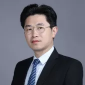
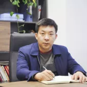
Leading YES’s efforts in India will be Dr. Ankineedu Velaga, a high-tech engineering executive with more than 35 years of experience spanning engineering and fab operations, customer interaction and retention, and business development support in the US and Asia.

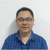
“Ankineedu’s experience in driving teams to improve processes will be a great resource for YES as we scale to meet the challenges of worldwide growth. We will be looking to him to draw upon his impressive track record of building organizations to develop complex semiconductor capital equipment as well as leading organizations to achieve better process development, yields, process control, cycle time, cost, and product quality,” said Rezwan Lateef, President of YES.

Dr. Velaga has held leadership roles with BRIDG, imec, SilTerra, Applied Materials, Avago, and Lucent (among others), and his global management experience extends from the US and the European Union to Malaysia and Singapore. His educational background includes a Ph.D. in Chemical Engineering from the University of Arkansas, an M.S. in Chemical Engineering from the Indian Institute of Technology in Madras, and a B.S in Chemical Engineering from the Regional Engineering College in Warangal, India.

“I am pleased and honored to be embarking on this exciting endeavor with YES,” commented Velaga. “We expect to build our India team quickly, and I look forward to talking with high-potential candidates. To see our current job postings for YES India, please visit Careers at yieldengineering.com and scroll down to the ‘YES India’ heading. If you don’t see a job there at the moment that aligns with your skills and interests, but you are a qualified candidate with a technical background and semiconductor experience, I encourage you to submit your resumé to [email protected] and include ‘YES India’ in the subject line.”

About YES
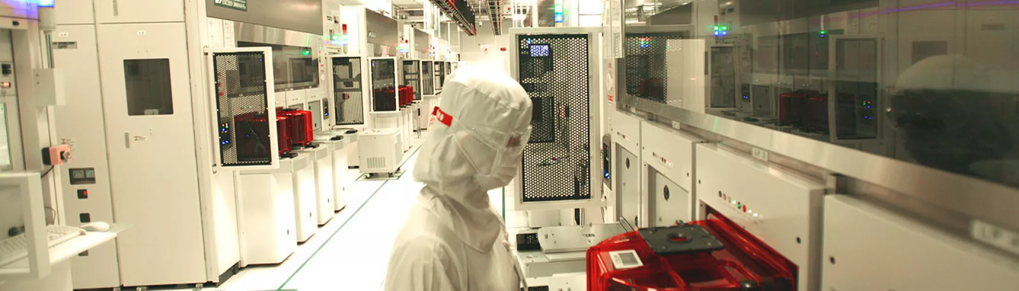
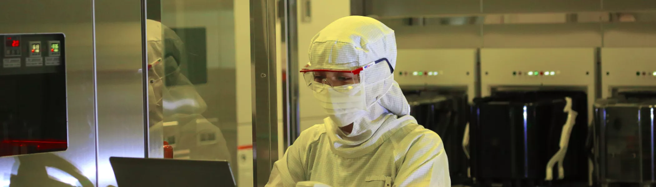
YES (Yield Engineering Systems, Inc.) is a preferred provider of high-tech, cost-effective equipment for transforming surfaces, materials, and interfaces. The company’s product lines include thermal processing systems, chemical vapor deposition (CVD) systems, plasma etching tools, and wet process equipment used for the precise surface modification of semiconductor substrates, semiconductor and MEMS devices, and biodevices. With YES, customers ranging from startups to Fortune 100 companies can create and volume-produce products in a wide range of markets, including Advanced Packaging, MEMS, Augmented Reality/Virtual Reality and Life Sciences. YES is headquartered in Fremont, California, with a growing global presence. For more information, please visit www.yieldengineering.com.

Heidelberg/Würzburg – "1 - 10 - 100 - 1000" – Achievable component heights of over 1 cm, surfaces with roughness in the order of 10 nm, structure sizes of less than 100 nm, and writing speeds over 1000 mm/s: At the SPIE Photonics West in San Francisco, from January 25th to 27th, Heidelberg Instruments will be presenting, for the first time, the new two-photon polymerization MPO 100, a multi-user tool that combines both the requirements of 3D lithography with resolutions in the 100 nm range and 3D microprinting with structure heights of over one centimeter, all in one device.

"The MPO 100 is a unique tool for microfabrication and achieves the highest resolution among additive manufacturing processes at 100 nanometers. Furthermore, the 1-10-100-1000 capability of the MPO 100 will enable users at universities, R&D institutions, as well as the industry and offer significant advantages for new developments in areas such as micro-optics, microfluidics, and biomedicine," says Dr. Benedikt Stender of Multiphoton Optics GmbH, the subsidiary of Heidelberg Instruments where the development of the MPO 100 was carried out.

The MPO 100 works with a laser wavelength in the green spectral range, which is ideally suited for the 3D structuring of typical photoresists. Furthermore, MPO 100 is optimized to use the hybrid polymers (ORMOCER®s), particularly important for various applications. In addition to sophisticated algorithms to maximize structure quality, the synchronized scanning system offers the possibility of stitching-free patterning. In addition, the MPO 100 is currently the only tool in the market equipped with a flowbox that guarantees temperature stability of up to 0.1°C and thus provides the necessary stability for large-scale exposures. Application-specific writing modes enable customer-specific printing requirements and distinguish the MPO 100 as a multi-user tool.

"With the MPO 100, we have combined the strengths of both companies in one system: Multiphoton Optics' sophisticated exposure unit for two-photon polymerization and Heidelberg Instruments' industrial platform, which guarantees the required stability and meets the necessary industry standards. The capabilities of the MPO 100 are already very popular with our customers, who benefit from the worldwide support from our service organization and ISO-certified production," says Steffen Diez, COO of Heidelberg Instruments.

Contact for further questions:
Veronika Loose, Marketing and Communications
[email protected]
+49 931 90879288

More information:
https://heidelberg-instruments.com/
https://multiphoton.de

About Heidelberg Instruments Mikrotechnik GmbH
With over 35 years of experience and more than 1,000 installed systems, Heidelberg Instruments is one of the leading international players in the development and production of high-precision photolithography systems and nanofabrication tools. Heidelberg Instruments systems are installed in industrial and scientific facilities around the world. They are used for efficient direct writing, as well as for photomask fabrication for a wide range of industries - including semiconductors, quantum computing, photonics, 2D materials, IoT, and many related application fields.

About Multiphoton Optics
Multiphoton Optics GmbH, a wholly owned subsidiary of Heidelberg Instruments Mikrotechnik GmbH, is a global solution provider for 3D lithography via two-photon polymerization (TPP). This disruptive technology enables the production of complex functional structures in micro-optics and microsystems technology, optical interconnect technology, micromechanics, and biomedical technology. The modular 3D printing platform enables the high-precision fabrication of structures in the submicrometer to millimeter range with very high throughput.

ESPOO, Finland, 3rd of February 2022 – Picosun Group and Shincron Co., Ltd. have joined forces for development and commercialization of Atomic Layer Deposition (ALD) for optical coatings. ALD technology provides uniform and conformal coatings to the even most challenging structures and is therefore well suited for high-end optical applications.

The R&D teams from both companies have worked together to tailor existing ALD processes optimizing them for the use in optical applications. In addition to standard ALD optical films, ALD magnesium fluoride (MgF2) has been researched and is now available for commercial use for the first time. So far, ALD MgF2 processes have been only presented in academic research by universities and science institutes. MgF2 is a desired material in optical applications due to its low refractive index at visible light and high transmittance in FUV optical region. It can be used as a single layer or as part of an optical stack combining low and high refractive index materials. It has also other features, such as barrier properties and high chemical stability, which bring big advantages in some applications.

The collaboration agreement was first signed in 2019 including the appointment of Shincron as Picosun’s sales representative and ALD product distributor in Japan. The collaboration was extended with Joint Development Agreement (JDA) in 2020 with the aim to develop novel and advanced ALD coatings for optical applications.

“We are very excited about the collaboration. The teamwork has been fruitful, and the results obtained now are excellent. We see optical coatings as one of the emerging ALD applications and believe in strong growth in this market”, says Jussi Rautee, CEO of Picosun.

“We are happy to add ALD technology to our offering. This way we can increase our services for our customers. We have set up a demo capability for ALD optical coatings and Japanese optical companies have shown high interest for this process”, says Masaya Narita, CEO of Shincron.

Read more: picosun.com/optics/magnesiumfluoride

More information:
Jussi Rautee
CEO, Picosun Group
Tel: +358 50 345 4457
Email: [email protected]
www.picosun.com

Masaya Narita
CEO, Shincron Co., Ltd.
Tel: +81 45 650 2411
Email: [email protected]
www.shincron.co.jp/en/

About Picosun
Picosun provides the most advanced ALD (Atomic Layer Deposition) thin film coating solutions for global industries. Picosun’s ALD solutions enable technological leap into the future, with turn-key production processes and unmatched, pioneering expertise in the field – dating back to the invention of the technology itself. Today, PICOSUN® ALD equipment are in daily manufacturing use in numerous leading industries around the world. Picosun is based in Finland, with subsidiaries in Germany, USA, Singapore, Japan, South Korea, China mainland and Taiwan, offices in India and France, and a world-wide sales and support network. Visit www.picosun.com.

About Shincron
Shincron is a leading global supplier of innovative vacuum thin film deposition equipment. Visit www.shincron.co.jp/en/ for more information.

China
Highlighted content

Shanghai
China

Standards

SEMI China ABFI TF Meeting

先进后道工厂集成工作组会议


Date: February 11, 14:00--15:30

Web Meeting link:Click here

2:00 pm - 3:30 pm Off Add to Calendar 2022-02-11 14:00:00 2022-02-11 15:30:00 SEMI China ABFI TF Meeting SEMI China ABFI TF Meeting 先进后道工厂集成工作组会议   Date: February 11, 14:00--15:30 Web Meeting link:Click here Shanghai China SEMI.org [email protected] America/Los_Angeles public

REGISTRATION

China CSM forun Business Executive Expositions Technical

Traffic Reminder

Venue: 2F International Conference Room, A2 Building of Guangda We Valley (Headquarters 2nd Road, Songshanlake, Dongguan City, Guangdong Province)

  • Venue to Humen Railway Station 22 miles, 45 minutes’ drives.
  • Venue to Shenzhen Bao'an International Airport 55 miles, 65 minutes’ drive.
Highlighted content

China

8:30 am - 9:00 am

Registration

9:00 am - 9:15 am

Opening Remark

9:15 am - 9:45 am
wang jiangbo
Jiangbo Wang
Vice President
HC SemiTek Corporation

Key Technologies for Mass Manufacturing of MicroLEDs

9:45 am - 10:15 am
Neng Zhang
Neng Zhang
Product Director
Sinopatt Technology Co.,Ltd.

Application and Developing Trend for Patterned Sapphire Substrate

10:15 am - 10:45 am
Qian Fan
Qian Fan
Vice President
Suzhou HanHua Semiconductor Co.,Ltd

Applications and Prospects of 3DIC Technology in Compound Semiconductor Devices

10:45 am - 11:15 am
Liang Wu
Jason Wu
CEO
Ultratrend Technologies Inc.

Latest Progress and Challenges on High-quality and Large-size AlN Single Crystals Grown by the PVT Method

11:15 am - 11:45 am
Yang Wang
Yang Wang
Vice Director
Songshan Lake Materials Laboratory

Micro&Nano Fabrication Platform of Compound Semiconductor Materials and Devices

11:45 am - 1:30 pm

Break

1:30 pm - 2:00 pm
Tiejun Zhou
Terry Zhou
GM
Vital Micro-Electronics Technology Co., Ltd

Processing and Application Prospectives of Large-Scale Compound Semiconductors

2:00 pm - 2:30 pm
Zhengwei Chen
Zhengwei Chen
GM
Beijing Ming Gallium Semiconductor Co., Ltd.

Industrialization Analysis of Ultra-wide Bandgap Semiconductor Material Gallium Oxide and Its Devices

2:30 pm - 3:00 pm
De'ang Liu
De'ang Liu
Scientist
ETARESEARCH

HVPE Growth of 4 Inch GaN Freestanding Wafer

3:00 pm - 3:30 pm
Kangfu Ma
Kangfu Ma
GMA
Shanxi Shuoke Crystal Co.,Ltd.

Analysis of SiC Single Crystal Growth Technology and Application Prospect of SiC Materials

3:30 pm - 4:00 pm
Yong Ji
Yong Ji
CEO
Guizhou Haotian Optoelectronics Technology Co.,Ltd.

Large Scale Deposition Technology of AlN and AlScN for SMR BAW

4:00 pm - 4:30 pm
Zhang Xing
Xing Zhang
CEO
Compound Semiconductor (Xiamen) Technology Co., Ltd.

The Latest Progress in The Industrialization of Diamond Wafer and Diamond Heat Sink

Standards Workforce Development

Compound Semiconductor Materials Technology Forum

Time: TBD

Location:Dongguan, Guangdong, China


Event Contact information:

Cassie Li

SEMI China

Email: [email protected]

Phone: 86.21.6027.7645


Ein Wu

SEMI China

Email: [email protected]

Phone: 86.21.6027.8509

8:30 am - 5:00 pm Off Add to Calendar Disabled
Event format

Registration

If you are SEMI Standards program member, please register here.

China PV and PV Materials China Joint TC Chapter Spring Meeting 2022
Highlighted content

Virtual
China

Standards

SEMI International Standards Program
PV and PV Materials China Joint TC Chapter Spring Meeting 2022
Friday, April 15, 2022
09:30-17:00
Virtual Meeting link:Click here


Agenda

09:00 – 09:30 Registration

09:30 – 09:50 Welcome & Call to Order

09:50 – 10:00 Review and Approval of Previous Meeting Minutes

10:00 – 10:05 SEMI Staff Report

10:05 – 10:10 Liaison Reports

10:10 – 11:10 Task Forces Reports

11:10 – 11:15 SEMI China PV TC Published Standards Announcement

11:15 – 12:00 Request for Global Ballots Cycle

13:30 – 16:15 Ballots Review

16:15 – 16:20 New Action Items & Update

16:20 – 16:30 Next Meeting Date & Locale


Standards Contact information:
Isadora Jin
SEMI China
Email: [email protected]
Phone: 86.21.6027.8578

9:00 am - 5:00 pm Off Add to Calendar 2022-04-15 09:00:00 2022-04-15 17:00:00 PV and PV Materials China Joint TC Chapters Spring Meeting 2022 SEMI International Standards Program PV and PV Materials China Joint TC Chapter Spring Meeting 2022 Friday, April 15, 2022 09:30-17:00 Virtual Meeting link:Click here   Agenda 09:00 – 09:30 Registration 09:30 – 09:50 Welcome & Call to Order 09:50 – 10:00 Review and Approval of Previous Meeting Minutes 10:00 – 10:05 SEMI Staff Report 10:05 – 10:10 Liaison Reports 10:10 – 11:10 Task Forces Reports 11:10 – 11:15 SEMI China PV TC Published Standards Announcement 11:15 – 12:00 Request for Global Ballots Cycle 13:30 – 16:15 Ballots Review 16:15 – 16:20 New Action Items & Update 16:20 – 16:30 Next Meeting Date & Locale   Standards Contact information: Isadora Jin SEMI China Email: [email protected] Phone: 86.21.6027.8578 Virtual China SEMI.org [email protected] America/Los_Angeles public