downloadGroupGroupnoun_press release_995423_000000 copyGroupnoun_Feed_96767_000000Group 19noun_pictures_1817522_000000Member company iconResource item iconStore item iconGroup 19Group 19noun_Photo_2085192_000000 Copynoun_presentation_2096081_000000Group 19Group Copy 7noun_webinar_692730_000000Path
Skip to main content
Default Banner Image

semiconductor manufacturing

Now, more than ever, semiconductor companies are relying on their human resources departments to ensure employee safety, support facility access and hygiene measures, cope with staffing demands and incorporate the rapidly evolving guidelines from Centers for Disease Control and Prevention (CDC) and the local state and city mandates. SEMI spoke with Crystal Reich, HR manager at X-FAB Texas, about her participation in the Fab Owners Alliance (FOA) human resources group and the value of collaborating with industry peers on a broad spectrum of topics: from focusing on specific areas such as ensuring employee safety and managing the workforce during a pandemic, to addressing broader organizational challenges such as benchmarking activities and identifying compensation and staffing best practices. SEMI: How did you learn about the FOA human resources group? Reich: I have been part of the FOA HR group since its inception in 2012. Lloyd Whetzel, the CEO at X-FAB Texas, has been very involved with the FOA for several years. When this group was being formed, he let me know about it. I came to the first meeting and have been a part of it ever since. SEMI: What does your participation in the FOA human resources group allow you and your company to do differently? Reich: I am also involved with the Society for Human Resource Management (SHRM), but the FOA HR group provides an excellent opportunity for semiconductor industry HR professionals to collaborate. The group not only covers topics that are specific to the semiconductor industry but also discusses broader topics related to preserving employee well-being during unprecedented challenging times, managing negative emotions, establishing appropriate political expression policies, and creating safe spaces for dialogue. Also, the benchmarking has been fantastic, especially from a compensation and staffing standpoint. It allows us to identify best-in-class recruitment strategies, determine any shortfalls and use this information to improve employee onboarding and development. In addition to discussing these types of issues and trends, we compare and benchmark other HR issues such as policy deployment and legislative trends with colleagues in the industry. SEMI: What are some of the key topics and activities that the FOA HR group has helped you focus on? Reich: X-FAB has been involved in a variety of activities at SEMI. Through the SEMI High Tech U program, we have been able to help college-bound high school students in our community access STEM curriculum and explore careers in technology. We have devised more robust military outreach strategies with the help of the Veterans Program at SEMI, allowing us to recruit and retain excellent technicians from the military. Additionally, benchmarking activities within the FOA HR group have helped us improve our talent acquisition process - especially for positions which are challenging to fill. SEMI: The pandemic brought many significant and unprecedented challenges that affected business continuity. How did your company's participation in the FOA help you navigate these changes? Reich: The FOA has been a great help in addressing the challenges of the global pandemic across several operational collaborative teams. In the early days of the pandemic, as employees moved to remote work, FOA organized a forum that allowed members to share how they dealt with this transition. Constantly changing guidelines and protocols meant that FOA members leaned on each other more than ever to share best practices and lessons from new safety process implementations. FOA offered survey and area-specific team activities, cross-functional operational sessions, and round table discussions at its 2020 Q4 meeting, where members exchanged ideas on how business processes changed during this period and shared what they were doing to ensure business continuity. This provided another excellent opportunity for FOA members to benchmark best practices within the semiconductor industry. SEMI: Would you recommend your peers to join the FOA HR group? Reich: I would highly recommend HR colleagues in the semiconductor industry join this collaborative group. It is a great platform to share ideas, learn from each other, and benchmark with other colleagues in the same industry. The FOA HR Metrics survey is a comprehensive survey covering several different areas within the HR discipline such as compensation, learning and development, tool training, corporate social responsibility, and many others. True to the nature of the FOA, the survey is a result of the collaboration between several HR professionals from Device Maker member companies. Please contact Shilpa Talwalkar at [email protected] if you would like to participate. X-FAB is a member of the SEMI Fab Owners Alliance, an international group of semiconductor and MEMS fab managers and industry suppliers that meet regularly to solve common non-competitive manufacturing issues and improve their business results. Nishita Rao is senior product marketing manager at SEMI.
Read More
With each transition to a new technology node, fab requirements for metal and particle contamination become more stringent, posing challenges for existing coating methods such as anodization or plasma spray that may not provide complete protection against contamination especially on critical chamber components with complex geometry. SEMI spoke with Beneq business executive Sami Sneck about common metal and particle contamination issues with critical chamber components, coating methods to protect against corrosion, and properties to look for when selecting the optimal protective coating solution. Sneck discussed the unique benefits of atomic layer deposition (ALD)anti-corrosion coatings with Aluminiumoxide (Al2O3) and Yttrium Oxide (Y2O3) and offered recommendations on how to work with original equipment manufacturer (OEM) partners to design, test and implement an ALD coating solution for semiconductor equipment. To learn more, visit Beneq at its digital booth at SEMI Technology Unites Global Summit, available on-demand until March 26, 2021. Registration is open. SEMI: How does ALD compare with other coating methods such as anodization and plasma spray? 
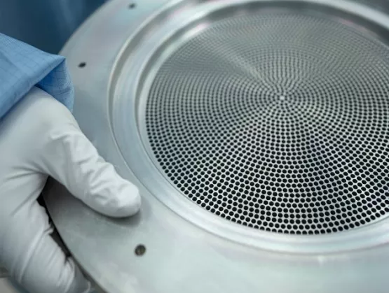
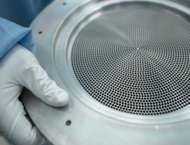
Sneck: ALD enables conformal dense and pinhole-free coatings on complex shapes. We can deposit various ALD coating materials on parts made of various materials. All other coating techniques have limitations. For instance, anodization is conformal, but porous and is suitable for Al2O3 used for aluminum parts. Plasma Spray is a line-of-sight method and not conformal on complex shapes, such as holes in showerhead parts. SEMI: Which substrate materials work for ALD coatings? Sneck: In general, parts made of common metal materials, such as aluminum, stainless steel or titanium, all work well with ALD coatings. Commonly used ceramic materials work well with ALD too. Plastic materials need to be coated generally at a lower temperature, which limits the coating material selection, but materials such as Al2O3 can be applied as well. SEMI: What is the maximum coating thickness you can reach with ALD? Does this depend on the material? Sneck: Yes, indeed. The maximum coating thickness does depend on the material of the part that we are coating. Polymer materials for example, have a very large coefficient of thermal expansion, which limits the practical coating thickness to the 100-nanometer level. On metal and ceramic parts, coatings of several micrometers are possible too. Typically, ALD coating thickness on chamber components range from a few hundred nanometers to one micrometer. SEMI: Which aspect ratio can you coat with ALD? Sneck: Basically, ALD can coat aspect ratios of 1000:1, but this would be extremely slow. In practice, some of the most complex parts are showerhead parts with small holes. Typically, these have an aspect ratio of around 100:1, which is perfectly commercially feasible for ALD. An extreme example would be gas lines: In this case, the aspect ratio may be also around 100:1, but the physical distance from one end to the middle may be half a meter. In this respect, it is not practical to wait for gas diffusion to reach such a depth level. Instead, the gas lines can be coated by forcing the ALD precursor gas flow into the gas line parts. This works well but needs part-specific manifolds to guide the gases. SEMI: What is the lifetime of ALD coating compared to other coatings? Sneck: ALD coatings differ from other coatings a couple of ways. First of all, ALD coatings generate less particle contamination since they are non-porous. Secondly, and most importantly, ALD coatings can cover areas that other coatings cannot. What is considered the lifetime of a certain part depends on various factors. Ultimately, the lifetime needs to be confirmed by testing parts in actual process chambers by running a lot of wafers through the chamber and monitoring critical parameters such as particle level and yield. SEMI: If you have multiple shelves with parts in the reaction chamber, how does the shelf position affect the coating uniformity? Is center shelf better than top and bottom shelf? Sneck: Uniformity depends on many parameters, including the part geometry, part holder geometry, batch size and coating material. When the shelves supporting the parts are optimally designed and the gas flow is well-distributed to all shelves, all shelves from top to bottom show similar uniformity. SEMI: Is there any risk of cross-contamination? Sneck: Cross-contamination could potentially be caused by the parts themselves or by different coating materials. The batch setup is fixed in production use, which means the parts are the same in every batch. The only variation is that the batch may not be full in some cases, but then we do not fill the empty part of the batch with other parts that could cause contamination in order to prevent contamination from one part type to another. Cross-contamination from one coating material to another is not a usual concern but can be prevented by using dedicated reaction chambers for different coating materials. This is very easy to do with Beneq P800. Sami Sneck manages Beneq’s semiconductor part coating business. He joined Beneq in 2005 and since then has held various professional and management positions including product manager, application manager, director of ALD group, head of sales, and head of Asia. He earned his MSc degree in Chemical Engineering in 2001 from Helsinki University of Technology. Sneck has special expertise in Atomic Layer Deposition technology and business development. He has played a vital role in introducing various ALD production concepts and solutions to several industries ranging from jewelry to photovoltaics, electronics and semiconductors. Access the free webinar recording and discover the latest anti-corrosion coating solutions and the unique benefits of ALD (atomic layer deposition). This webinar is particularly helpful for process engineers, equipment engineers and others responsible for contamination control and equipment yield. Serena Brischetto is senior manager of Marketing and Digital Engagement at SEMI Europe.
Read More
The work of the SEMI Environment, Health and Safety (EHS) COVID-19 working group to address industry EHS issues and share best practices has morphed as rapidly as COVID-19 itself as the vaccine rollout continues, inspiring new hope for a return to normal. The group has evolved from mounting crisis responses to urgent issues such as the shortage of masks and sanitization wipes and sprays to helping companies prepare for their employees’ return to the workplace and developing on-site health-screening procedures for employees and visitors to help ensure their safety. Hot SEMI EHS COVID-19 working group topics have included the following as the team continues to meet every other week to stay abreast of COVID-19 developments and their industry impacts. Vaccinations SEMI members have been monitoring the progress of U.S. states and counties in delivering vaccines. So far, no essential workers in the electronics industry have been eligible to be vaccinated. To help gauge the availability of vaccines to essential industry workers, some companies have hired external consultants to monitor the phase-in. The SEMI EHS COVID-19 working group will collect and centralize the information to help members plan for their employees’ return to the workplace. Policy Enforcement At manufacturing sites, some employees reportedly are becoming complacent in following masking and distancing policies, prompting reminder communications from top management for workers to comply until the pandemic is brought to heel. The higher-ups are also encouraging staff to get vaccinated once they are eligible, with some member companies offering workers time off or other incentives for their employees and families to get vaccinated. Contact Tracing Despite the intense focus on contact tracing since the initial COVID-19 outbreak last year and early efforts to track people movement using smartphone applications or wearables, no tracking technology has emerged as the standard for helping to curb the virus’s spread. SEMI members have been testing various technologies ranging from Bluetooth to wearables with wide-band radio waves to track employees while on site. Tracing by wearables has proven inaccurate. Left with no better alternative, the vast majority of SEMI members are performing time-consuming manual contact tracing. OSHA Compliance While OSHA has picked up the pace in issuing new regulations related COVID-19, pandemic-related site inspections have lagged, some SEMI working group members report. In California, CAL/OSHA recently passed a COVID-19 Preparedness Plan that defines the responsibility of employers in preventing workplace outbreaks, offering PPE to workers and conducting frequent testing. The California plan mirrors the CDC recommendations implemented at the onset of the pandemic. To join the SEMI EHS COVID-19 working group, contact our EHS team at [email protected]. Olivier Corvez is senior manager of Environment, Health, Safety and Sustainability at SEMI.
Read More
International Women’s Day (IWD) is a global day celebrating the social, economic, cultural and political achievements of women. The day is not only the centerpiece of the movement for women’s rights but a unique opportunity to recognize the contributions of women to the semiconductor industry. The first International Women’s Day took place in 1911 when more than a million people in Austria, Denmark, Germany and Switzerland marched to demand equal rights for women including the right to vote and to protest employment sex discrimination. In 1977, the United Nations General Assembly invited member states to proclaim March 8 the UN Day for women's rights and world peace. In recent years, organizations and companies worldwide have sought to use IWD to celebrate the contributions of women to our homes, families, workplaces and communities. The IWD theme for 2021 is Choose to Challenge – a call to draw attention to women’s inequality. It’s also an excellent opportunity for all SEMI members to choose to challenge deep-rooted thinking and behavior in order to grow diversity and collectively commit to increasing the representation of women and women-owned businesses in the semiconductor industry. The double-edged challenge for the chip industry is to grow the ranks of women while retaining those now in the workforce. One in four women are considering leaving their workplaces or downshifting their careers due to work-life challenges stemming from COVID-19, SEMI noted in a recent blog highlighting the Women in the Workplace 2020 study by McKinsey Company and LeanIn.org. One in four! In 2021 it’s important for us to recognize and work to reverse this trend by taking time to encourage, support and celebrate women in the face of COVID-19. A shining example of the enormous contributions to semiconductor industry by women is Dr. Suvi Haukka, a pioneer of atomic layer deposition (ALD) technology. Thirty years ago, Dr. Haukka spied a small note on a university noticeboard that led to her pursuit of a long and highly distinguished career in our industry. The note was a job opportunity with ASM International to research ALD, a role she landed. Upon joining ASM, Dr. Haukka investigated the use of ALD for catalysis applications to modify porous high-surface area materials used in oil refining and polymerization. What was initially a niche application to modify the surfaces of microporous substances and silicon solar cells evolved over time to become a critical materials technology and manufacturing method for coating semiconductor wafers. Working systematically in the lab, Dr. Haukka and her coworkers made fundamental materials and manufacturing process discoveries that advanced ALD material science and manufacturing technologies. An accomplished inventor and technical contributor, Dr. Suvi Haukka was named ASM’s very first Fellow of the Technical Staff in 2018. “Being named an ASM Fellow was a huge moment that made me very, very proud,” Dr. Haukka said. “I have spent my entire professional career working with ALD, and I have been very fortunate to work with many talented colleagues at ASM. “Together we have dedicated ourselves to introducing ALD as a standard means of manufacturing in the semiconductor industry. I believe the award is in recognition of all the valuable work we’ve done over the years.” Dr. Haukka is ASM’s most prolific inventor with more than 100 patents to her name. Her remarkable contributions to the development of ALD chemistry and semiconductor manufacturing process technologies over her three-decade career have made her a highly respected, internationally recognized researcher in the semiconductor manufacturing industry. Bill Olson is the corporate responsibility and conflict materials lead at ASM International N.V. in Phoenix, Arizona. He graduated from the University of Wisconsin-Madison with a Ph.D. in Inorganic Chemistry. Bill has 23 U.S. patents and has published more than 40 technical articles. He can be reached via LinkedIn at www.linkedin.com/in/williamolson.
Read More
The SEMI Smart Manufacturing Americas Chapter, a key driver of the Global Smart Manufacturing Initiative, accelerates awareness of digital and data-driven strategies and implementations to help speed adoption of smart manufacturing. In 2021, the Chapter will focus on expanding its work across the industry to include academic and research initiatives. The semiconductor industry saw an unprecedented focus on improving digital monitoring of manufacturing activity in 2020, partially due to COVID-19. The Americas Chapter shared case studies on new tools and techniques for social distancing in fabs, aides for remote maintenance, and tips for remote workers. The Chapter also introduced its three pillars of Sensing, Connecting and Predicting and offered related programs. The Global Smart Manufacturing Conference (GSMC) highlighted the significance of universities and research institutions in the development of smart manufacturing with their focus on joint research for broad dissemination. To help drive smart manufacturing advances, at GSMC several offered non-proprietary tutorials on topic including the following: Integrating sensors for acquisition – CEA-Leti Applying new AI and ML tools and strategies to manufacturing – Binghamton University Digital tools for planning, qualifying and management and scheduling in fabs – MINES Saint-Étienne. Adding AI tools to robot work in a smart factory – KAIST Institutes By continuously highlighting the activities of these and other institutions through presentations, interviews, articles and blog posts, we will draw more attention to what is on the horizon for smart manufacturing in 2021. The SEMI Smart Manufacturing Americas Chapter also plans to elevate activities important to the Outsourced Semiconductor Assembly and Test (OSAT), Surface-Mount Technology (SMT) and Printed Circuit Board Assembly (PCBA) segments of the industry including programs on inspection, traceability and the SEMI SMT-ELS Standard for SMT automation. Thurston Taylor, marketing expert at Tokyo Electron and Vice Chair of the Americas Chapter, notes that “With increasingly more demanding requirements for bump, assembly and test, smart manufacturing and applied data science are necessary to achieve back-end goals now and in the future.” Also, many companies are implementing smart manufacturing applications and assessing various strategies to increase their smart manufacturing capabilities. Members of the Americas Chapter plan to review and develop self-assessment documents and maturity models that apply to front-end wafer fabs all the way through packaging and assembly facilities. “Moving forward it is imperative for all of us to up the intensity on specific ROI vectors such as quality, cost, productivity, sustainability and safety leveraging our smart manufacturing SEMI framework of Sensing, Connecting and Predicting,” said noted Bobby Mitra, worldwide director of Smart Manufacturing at Texas Instruments and Americas Chapter Chair. “By offering special flagship events, invited talks, ROI case-studies and ROI criteria in maturity models, we’ll bring high value to the smart manufacturing industry.” Chapter members also will begin mapping the skills needed to implement and support increasingly digital manufacturing capabilities, including any new skill sets, to help companies develop their hiring, training and management strategies. The mapping effort aims to support companies in building a strong pipeline of employees who can efficiently manage and operate smart manufacturing facilities. For its part, the Americas Chapter’s Go Green Subcommittee will focus on applying smart manufacturing technology to reducing the electronic industry’s carbon footprint by accurately tracking energy waste improving overall fab efficiency. Stay tuned for details on activities planned for our chapters in Europe, China, Japan, Korea, Southeast Asia and Taiwan. To learn more about each chapter and how to get involved, please visit the SEMI Smart Manufacturing Hub and sign up for our newsletter. Ayo Kajopaiye is senior project coordinator, Collaborative Technology Platforms, at SEMI.
Read More
Despite the pandemic lock-down, demand for electronic products and services remains strong. Work-from-home, video conferencing, and remote learning are driving data center growth and laptop and tablet demand. 5G infrastructure rollout is underway and smartphone sales are returning to normal levels. Automotive sales are increasing. At the same time, the industry is experiencing acute shortages of substrates. The October 2020 fire at Unimicron’s IC package substrate plant in Taiwan exposed the serious nature of the capacity shortage for IC package substrates. Substrate makers have been reluctant to make large investments in capacity over the last few years due to the fear that demand could decline and they would have excess capacity. Relentless price pressures by customers and the resulting low margins have weakened the finances of substrate suppliers. With tight capacity, substrate prices have increased and lead times are 14 weeks or more. The most critical shortage is for flip chip ball grid array (FC-BGA) substrates. In addition to increased demand in units, applications such as servers and networking products are seeing requirements for larger body sizes and increased layer counts. Shortages will not improve very soon because it takes time to build a new plant. And equip it. Key equipment for substrate production has lead times of up to a year. SEMI and TechSearch International detailed the substrate makers and provide projections for the substrate market, trends, and a list of suppliers and their plant locations in the Global Semiconductor Packaging Materials Outlook report. The report also highlights the market and suppliers for leadframes, bonding wire, encapsulation materials, underfill, die attach, solder balls, wafer level package dielectrics, and wafer-level plating chemicals. In times of shortages the report is an important indicator of suppliers in the industry and trends. Jan Vardaman is President at TechSearch International Inc.
Read More
Nikki Zaahir joined SEMI last year as senior program administrator on the SEMI Works team after spending the last 15 years designing, coordinating and directing programs that help people develop job skills and find full-time employment. Her career includes roles at the Department of Defense, the National Security Agency, America Works and Vehicles for Change.I spoke with Nikki about her passion for workforce development as we celebrate Black History Month.Williams: What does Black History Month mean to you?Zaahir: Black History Month means to me an opportunity to highlight the overwhelming influence of the inventions that Black Americans contributed to this country. Of all the Black history shared this month, it’s the inventors that have always intrigued and excited me the most. I grew up in a home with parents that taught my siblings and me the history of our culture every day. However, each February I was allowed to research and share my own list of what we called “little known Black history facts.” A couple of my favorites from my childhood are Lonnie Johnson, who invented the Super Soaker water gun, and Alexander Miles, who developed automatic elevator doors in 1887. Frankly, Black History Month reminds me to be proud to be Black and to take a moment to pay homage to the excellence and fortitude of my people.Williams: Where are you from, and where did you go to school?Zaahir: I am from the suburbs of Maryland right outside of Washington, D.C. I grew up in a military family. My father was the first black 1st Sargent in his transportation company. His unit was responsible for transporting heavy artillery equipment around the world. I went to Meade Senior High School on the army base of Fort Meade.Williams: How did you get started in the semiconductor industry?Zaahir: While in the 11th grade, I was actively recruited by a semiconductor company that had recently won a National Security Agency government contract at Fort Meade to make semiconductors for the military.I excelled in English and Science and met the requirements for the work study, which allowed me to spend half of my day in school and the other half at a work study assignment. The company tested a couple of hundreds of students and I was one of the 34 chosen for the career development program. I worked as a technician responsible for the fabrication and processing of the semiconductor wafer. My favorite steps of this process were the spin on glass and gasses chambers in the fab. What lit a fire in me was the realization that there is a whole world of technology opportunities that people like me were unaware of.Nikki Zaahir, in her former role as National Director of Workforce Development and Training at Vehicles for Change, with interns training to be certified automotive technicians.Williams: Did you have any mentors or sponsors who were particularly meaningful as you developed your career?Zaahir: I’ve been very fortunate to be mentored and supported by many people on my professional journey. Peter Cove and Dr. Lee Bowes are a social activist couple who own America Works. They were instrumental in my understanding of workforce development by teaching me that self-sufficiency through gainful employment can change generational poverty. However, the most meaningful people to me are those whose lives I’ve had the absolute pleasure to help change. For example, at Vehicles for Change, I created a social enterprise designed to assist returning citizens (people formerly incarcerated) with training and job placement. In three years, we placed 200 men and women in the workforce with no one reoffending or returning to prison within three years. What made this group of individuals special is that I chose to focus on violent offenders that served 10 years or more in prison.Williams: What motivates you in your work?Zaahir: What drives me is helping people become aware of careers that could not only change their lives but the lives of their families, and waking up every day determined to be that conduit of information and job opportunities.Williams: What is wonderful and challenging about workforce development?Zaahir: Inspiring people to consider educations and careers that may have never been on their minds is the most rewarding aspect of workforce development. To see people who have felt left out of training and employment opportunities due to their backgrounds or lack of higher education take charge and pursue educations and careers that before were only a dream makes this work worth it. On the other side of that, convincing someone who has felt left behind or unworthy of a better life for themselves and their family can be challenging.Williams: Is there a particular story about someone you’ve worked with or helped that you’d like to tell?Zaahir: Eight-time Grammy award winning artist Lauryn Hill of the legendary hip hop group The Fugees once said “In my travels all over the world, I have come to realize that what distinguishes one child from another is not ability, but access. Access to education, access to opportunity, access to love.”I have been blessed beyond measure to work with and help so many people at this point in my career. What I’d like to share is while talent is abundant, access and opportunity are not. That is the story.Williams: What is something unusual about you that people might not know?Zaahir: I’ve studied at the Arthur Findlay College, the world’s foremost college for the Advancement of Spiritualism and Psychic Sciences. Oh! the ghost stories I could tell.Williams: What would you tell young people interested in working in the semiconductor industry?Zaahir: In this industry, you will develop transferable skills for almost any career in manufacturing or production and the ability to make a salary that will provide the opportunity to afford living in safe neighborhoods, reliable transportation and vacations! You can pursue a wide range of skills, training, education and other professional development opportunities in this industry – all while maintaining a healthy work-life balance.Michelle Williams is deputy director of the SEMI Foundation.
Read More
In my role as lead for the Smart Mobility initiative at SEMI, I recently spoke with Automotive Logistics Magazine about the growing importance of the semiconductor supply chain’s connection with the automotive industry and the semiconductor shortage hampering global automotive production. Following are excerpts from the interview. Automotive Logistics: Why is there a bottleneck in the global supply of semiconductors at the moment and how long is it likely to last? Weiss: The current automotive chip shortage resulted from the sharp, Covid-19-induced decrease in demand for automotive semiconductors in the second quarter of last year when vehicle production came to a near standstill. The automotive market picked up significantly in the fourth quarter and this caused the supply chain constraints we are seeing today. At the same time as the automotive standstill, the pandemic spurred an increase in demand for home computing and networking equipment, and semiconductor manufacturing plants (fabs) had to pivot to these other markets in order to maximize fab utilization and successfully navigate economic headwinds. Every minute a semiconductor fab is idle or has lines down adds up quickly to missed revenue, so their capacity is booked weeks and even months in advance. With this background, I don’t believe this is a structural shortage and expect a gradual recovery over the next two quarters, barring any major shifts in geopolitics or macroeconomics. Automotive Logistics: What needs to be done to remedy the current shortfall for the automotive industry? Weiss: The automotive industry needs to continue to strengthen its connections to the semiconductor manufacturing supply chain. In past years, auto manufacturers used to rely mainly on their tier one suppliers to interface with the semiconductor supply chain. This has changed significantly. Not only are more chips being used in vehicles (roughly 10% of all devices produced globally end up in cars), but the strategic importance of the chips as enablers for ADAS [advanced driver-assistance systems], electrification, safety, connectivity and other consumer-driven features has increased considerably. With this dynamic in play, carmakers have recognized the value of interacting and collaborating more closely with the semiconductor supply chain. This provides vehicle OEMs with access to innovation, the ability to influence technology direction and pace, along with greater visibility into global supply chain developments. The SEMI Smart Mobility initiative is evidence of this transition, with the likes of Audi, BMW, Ford, Uber, Volkswagen and other vehicle OEMs, along with tier one suppliers such as Continental and Bosch, now actively involved in our automotive electronics and mobility activities to do exactly that – influence, partner, accelerate and guide the global electronics design and manufacturing supply chain that SEMI represents. Automotive Logistics: What percentage of semiconductors manufactured for use by US-based companies are for automotive applications and how has this grown in recent years? Weiss: A little over 10% of semiconductors produced worldwide are sold into the automotive segment, but this number is expected to grow at an accelerated pace in the next few years as electrification, connectivity and autonomous driving become more prevalent. Automotive Logistics: How is SEMI working to help the automotive industry get a clearer view of sub-component supply and better manage supply chain risk? Weiss: The SEMI Smart Mobility initiative is designed to engage automotive OEMs, tier ones, semiconductor device makers, design houses, and equipment and materials companies to drive alignment across the supply chain and address shared challenges collectively. To facilitate this engagement, we created the Global Automotive Advisory Council (GAAC), which has active chapters in Europe, US, China, Japan and Taiwan. The GAAC provides an open platform for creating solutions, fostering collaboration and partnering with other industry bodies to accelerate and harmonize industry efforts that benefit the entire ecosystem. Volkswagen and Audi are already SEMI members – both are founding members of the GAAC Europe chapter – and have become vocal champions and critical contributors to our efforts. When all stakeholders work together, I have no doubt that the future of automotive and mobility will continue to be bright. Interested in learning more about this topic? Read the full interview in Automotive Logistics Magazine, A Fab Future for the Automotive Sector. Please contact me at [email protected] for more information about SEMI’s Smart Mobility Initiative, the Global Automotive Advisory Council, and how SEMI can help your organization navigate electronics in the automotive industry to drive innovation in the mobility space. Bettina Weiss is Chief of Staff and Global Smart Mobility Lead at SEMI.
Read More
Ride the Wave of Smarter Manufacturing The year 2020 sparked a tremendous acceleration in the digital transformation worldwide, driving a sharp rise in demand for semiconductors and escalating pressure on chip factories to reduce manual functions on the shop floor. The mindset of the semiconductor industry saw a remarkable shift as it recognized with heightened urgency the need to deploy data-driven visualization, analysis, scheduling and dispatching solutions to increase automation to improve production speed and efficiency. Amidst the new excitement around Industry 4.0, chip manufacturers are rapidly deploying new technologies including IIoT, big data, machine learning and Autonomous Intelligent Vehicles (AIVs). Yet for many chip manufacturers, the path to building a smart factory is far from clear because they lack an overall digital transformation strategy. Smart manufacturing is a broad concept covering an array of technologies and solutions, making a holistic, mid- to long-term digitalization strategy rooted in the overall business strategy crucial. There are no shortcuts that can move a manufacturer instantly to Industry 4.0. Instead, this transformation is a step-by-step undertaking with a natural evolution. Some Factory Tasks Must Remain Manual – For Now The semiconductor industry has reached a point where manual processes are no longer efficient enough to support mass chip customization and remote operations. The many technological and standardization advances behind automation can help streamline some of a factory’s most labor-intensive tasks including the loading or unloading of machines or lot tracking and data collection while reducing operational costs. Still, some tasks remain very difficult to automate. For example, handling errors and exceptions presents the greatest challenge since some errors are hard to anticipate. What’s more, the cost of automating error handling can be prohibitive. Eliminating Gaps in Connectivity Often, critical data sources aren’t available due to lack of equipment integration, incomplete product quality monitoring or gaps in material tracking. Closing these gaps in connectivity enables the collection of data and provides rich, reliable information for analysis and reporting that can drive continuous operational improvements, optimizations and efficiencies throughout a factory. But keep in mind that data integration alone can be a challenging task. The selection and proper enrichment of relevant data is, in many cases, not just a technical problem but requires a detailed and in-depth knowledge of the manufacturing steps to be analyzed and optimized. Even when data is available, it might be still difficult to make decisions or implement improvements if it is in siloed systems that require manual processes to integrate and translate into useful information. Problem solving at this level is possible but extremely time-consuming. Manual integration is not only ineffective but costly, draining time, human resources and money from the factory. The right contextual information for the data is vital to unleash its potential and make improvements possible. Dispersed solutions cannot control processes because they span functional areas and people, physical and business entities. Backbone software for shop-floor operations that controls all other applications is central to smart manufacturing. Data-Driven Manufacturing The semiconductor industry is expert in data collection and leads many other industries in this area. The problem is often that chip companies use only a fraction of the information they collect for the analysis and insights needed to improve operational efficiency. By comprehensively integrating all distributed data into a single version of truth – in one location where it is always available – companies can make data analysis and problem solving almost frictionless. Keep in mind that data platforms and edge solutions, within the context of manufacturing, will not be adopted as part of a greenfield initiative. Building a solid automation architecture is only feasible and beneficial by deploying new technologies such as machine learning and artificial intelligence (AI). Analysis of historical data provides important context and reveals deviations such as unexpected process time, uncommon material accumulations or issues with material transport. By integrating swift control actions for new data point collected, manufacturing operations can shift from reactive problem-solving to proactive analysis and operational improvements. The tremendous increase in interest and investment in AI for manufacturing automation only became possible with the availability of low-cost sensors that generate huge volumes of data and solutions for storing and processing that at low cost. AI and other leading-edge technologies transform the tedious but critical process of extracting insights from data, making it instantaneous, streamlined and achievable for every manufacturer. The maturity of smart manufacturing hinges on the extent to which a factory is data-driven. This requires foundational investments to improve traceability, connectivity and real-time operations – and finally making sure that data helps us what to do and when to do it. Ricco WALTER is managing director of SYSTEMA Automation in Singapore.
Read More