downloadGroupGroupnoun_press release_995423_000000 copyGroupnoun_Feed_96767_000000Group 19noun_pictures_1817522_000000Member company iconResource item iconStore item iconGroup 19Group 19noun_Photo_2085192_000000 Copynoun_presentation_2096081_000000Group 19Group Copy 7noun_webinar_692730_000000Path
Skip to main content
Default Banner Image

Christian G. Dieseldorff

Back in 2012, China ranked fifth among seven regions worldwide in IC wafer capacity but surged past the Americas and Japan in 2018 and 2019 to claim the number three position (figure 1). That’s a big deal given that ICs account for the largest share of wafer capacity excluding discrete, opto, MEMS and sensors.China’s IC wafer capacity growth accelerated to tune of 14% in 2019 and 21% in 2020 and is expected to grow at least 17% this year, as we report in the latest update of the World Fab Forecast, published December 3rd by SEMI. Of all regions, Taiwan boasts the second strongest growth rate over the same period at 3% to 4%.Figure 1: Total IC installed wafer capacity for top five regions The report shows that from 2019 through the end of 2021 China will have increased wafer capacity for memory by 95%, foundry by 47% and analog by 29%. Foundry will represent the largest portion of those gains, reaching 2 million wpm (200mm equivalents). Memory will follow at about 1.5 million wpm and then analog at over 120,000 wpm.But Chinese companies aren’t pulling off this feat singlehandedly. Many international companies are contributing to the wafer capacity increases in China (figure 2). Figure 2: IC wafer capacity in China by company origin The share of capacity contributed by Chinese-owned companies and international companies has changed little since 2012, though Chinese-owned companies saw a slight dip in their slice of the pie from 60% to 57%From 2019 through 2021, Chinese-owned companies will add almost 60% capacity for foundries, the most of all sectors. Companies including SMIC, Hua Hong Semiconductor, Nexchip, XMC and Hua Li Microelectronics are driving the increases.During the same period, Chinese-owned companies will ramp up memory capacity from basically zero to 300,000 wpm. Companies such as Yangtze Memory Technology and ChangXin Memory Technologies (CXMT), also known as Innotron, are powering the quick rise with aggressive ramps of 3D NAND and DRAM capacity.Among international-owned companies, TSMC and UMC are driving the largest share of foundry growth, while Samsung, SK Hynix and Intel are powering gains in memory capacity.More information is available in the World Fab Forecast report. The report currently collects information for fab equipment and construction investment, capacities, technologies and product types for over 280 fabs and lines in China alone, including 40 facilities that either began operation in 2020 or will from 2021 through 2024.Christian G. Dieseldorff is senior principal analyst in the Industry Research and Analysis group at SEMI in Milpitas, California.
Read More
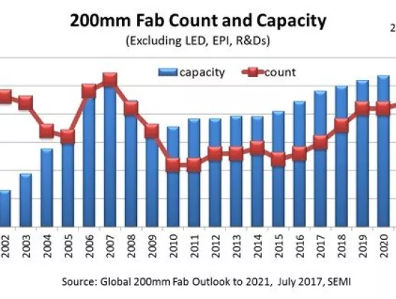
This year, SEMI ISS covered it all – from a high-level semiconductor market and global geopolitical overview down to the neuro morphic and quantum level. Here are key takeaways from the Day 1 keynote and Economic Trends and Market Perspectives presentations.In the opening keynote, Anne Kelleher from Intel pointed to the huge growth of data, with fabs collecting more than 5 billion sensor data points each day. The challenge, Kelleher noted, is to turn massive amounts of data into valuable information. Moore’s law is not dead. New models of computing benefit still from Moore’s law and advances in Si/CMOS technologies for conventional, deep learning, neuro morphic and quantum computing.With customers expecting continual improvements in applications, the question is whether the chip industry is moving fast enough to meet these expectations, Kelleher said. A broad supply chain, equipment and materials innovations, and attracting the “best of the best” college graduates to fuel innovation is key, she said.In the economic trends session, Nicholas Burns (ambassador ret.) from Harvard University pointed out that we will see a major shift in power. The U.S. will remain the major world power over the next 10 years, but we will see a major shift in power in the next coming decades as the gap with countries like China, Russia and India continues to narrow.Duncan Meldrum from Hilltop Economics said that we are passing the peak growth of economic cycle. He warns that a more likely outlook is that a global growth recession is developing. Although semiconductor MSI growth will see a noticeable slowdown in 2019 and 2020, the semiconductor industry is still healthy over the longer term.Bob Johnson from Gartner sees demand shifting from consumer to commercial applications with higher ROIs and budgets. AI, IoT and 5D are the major enablers. He sees structural changes in the semiconductor industry especially for memory but also for Moore’s law with increasing costs and fewer players.The DRAM markets shows volatility and NAND market may be negative in 2019 but non-memory are expected to accelerate mainly because of increasing content and some price hikes.Overall Gartner expects good long-term growth with a CAGR (2017 to 2022) of 5.1%, outpacing 2011 to 2016 CAGR of 2.6%. After a strong 2018 with 13.4% revenue, he forecasts a slower 2019 with 2.6% growth followed by a 8% growth in 2020 and negative growth rate in 2021.Andrea Lati of VLSI went “Back to fundamentals” in his presentation about the industry. VLSI sees a downside bias due to slowing global economy, tariffs, and trade wars. Future drivers are data economy, cloud, AI and automotive.As memory leads the 2019 slowdown, analog, power, logic and other sectors remain in positive territory. VLSI lowered its semiconductor equipment forecast for 2018 from 20% (Jan. 2018) to 14% (Dec. 2018) but increased its sales outlook from 8% to 15% in 2018. VLSI expects revenue to slow into the first half of 2019 but increase to over 4% in the second half of the year, resulting in total 2019 drop of 2.7%. Semiconductor equipment sales are expected to drop from 14% in 2018 to -10% in 2019.Michael Corbett of Linz Consulting, covering wafer fab materials in the years of 3D scaling, sees these as good times for the industry. His outlook for wafer fab materials is bullish based on strong MSI and because wafer fab materials suppliers are getting bigger because of M As.In the Market Perspective session, Sujeet Chand of Rockwell Automation pointed out that as more and more data is generated, the problem is how to get value of all the data collected. There is a need to create the right architecture for machine learning and AI and big data is increasingly being replaced by contextual/structured data. He expects Industry 4.0 to drive foundries to become smaller, more flexible and more productive.In the Technology and Manufacturing session, Aki Sekiguchi of TEL addressed process challenges in the age of co-optimization. The semiconductor industry continues to expand, driven by massive growth of interconnected devices, with heavy demand for processing power and storage. He expects an exponential increase of data from about 40ZB in 2018 to 50ZB in 2020 to 163 ZB in 2026.Major technologies such as DRAM, 3D NAND and logic are dealing with scaling challenges. The density of DRAM (Mb/chip) is plateauing according to 2015 to 2020 trend data, with DRAM is in need of EUV. Memory capacity demand is leading to increasing layers and higher aspect ratios that is concern for 3D NAND and mainly for plasma etch. With Logic already implementing 3D structures, it appears to be in a solid position. Buddy Nicoson of Micron talked about his 50 years in the industry and looked ahead to the next 50. The anchors – quality, cost, scale and speed – won’t change. It has been a great journey so far with unprecedented opportunities and challenges ahead of us. We are getting into a convergence (specialization, integration) and solution-based phase. We will see some inflection points in the coming years, with the best yet to come.Christian G. Dieseldorff is senior principal analyst in the Industry Research and Analysis group at SEMI in Milpitas, California.
Read More
Tracking toward even stronger growth than forecast last year, 200mm fabs worldwide are gearing up to add more than 600,000 wafers per month from 2017 through 2022, an 11 percent growth rate that will lead to a new high of 6 million wafers per month by the end of 2022, according to the SEMI Industry Research and Statistics group in its fourth update of the Global 200mm Fab Outlook report. See chart below. All told, 56 older and newer facilities will add capacity, with the MEMS, power, logic and foundry segments contributing the most. To help meet rising demand, new fabs are under construction. Only six facilities plan to reduce capacity. The global 200mm fab count will increase from the 2017 level of the 194 fabs covered in the report to 203 by 2022. See chart. During the five-year forecast period, China, at 44 percent, is expected to account for the greatest growth, followed by Southeast Asia (19 percent), Taiwan (10 percent) and the Americas (8 percent). However, with strong demand for new 200mm fab equipment, the used 200mm fab equipment market has pretty much dried up. What’s more, the availability of key tools and spare parts has become a primary concern for many device makers. These headwinds notwithstanding, many companies remain bullish with plans to add more capacity. The forecast growth of 600,000 wafers per month may ultimately be a conservative estimate. SEMI’s Global 200mm Fab Outlook report lists more than 300 facilities and lines managed by more than 150 companies, providing details on product type, investment, technology and capacity plans by companies and fabs. The fourth update of the Global 200mm Fab Outlook report covers data and predictions from 2011 through the end of 2022, including milestones, detailed investments by quarter, product types, technology nodes and capacities down to fab and project level. Click here for the Global 200mm Fab Outlook Sample Report. Learn more about other SEMI fab databases at www.semi.org/en/MarketInfo/FabDatabase. Christian G. Dieseldorff is director of Industry Research and Statistics, SEMI, Milpitas, California.
Read More
Christian G. Dieseldorff, Industry Research Statistics Group, SEMI (June 12, 2018)The semiconductor industry is nearing a third consecutive year of record equipment spending with projected growth of 14 percent (YOY) in 2018 and 9 percent in 2019, a mark that would extend the streak to a historic fourth consecutive growth year, according to the latest update of the World Fab Forecast report published by SEMI. The industry last saw four consecutive years of equipment spending growth in the mid 1990s.Korea and China are leading the growth, with Samsung dominating global spending and ascendant China on a fast, steep rise, surging ahead of all other markets. See figure 1.Figure 1: equipment spending by region (includes new and refurbished)Samsung is expected to reduce equipment investments in 2018. Despite the ebb, the company still accounts for a dominant 70 percent of all investment in Korea. At the same time, SK Hynix is increasing its equipment spending in Korea.China’s equipment spending is forecast to jump a whopping 65 percent in 2018 and 57 percent in 2019. Notably, 58 percent of investments in China in 2018 and 56 percent in 2019 stem from companies with headquarters in other regions such as Intel, SK Hynix, TSMC, Samsung, and GLOBALFOUNDRIES. Domestic, Chinese-owned companies – backed by large government initiatives – are building an impressive number of new fabs that will start equipping in 2018. The companies will double their equipment investments in 2018 and again in 2019.Meanwhile, other regions are also ramping up investments. Japan is beefing up equipment spending by 60 percent in 2018, with the largest increases by Toshiba, Sony, Renesas and Micron.The Europe and Mideastern region will boost investments by 12 percent in 2018, with Intel, GLOBALFOUNDRIES, Infineon and ST Microelectronics as the largest contributors. Southeast Asia will increase investments by more than 30 percent in 2018, although total spending is proportionately smaller than in other regions owing to its size. The main contributors are Micron, Infineon and GLOBALFOUNDRIES, though companies including OSRAM and ams are also increasing investments.The SEMI World Fab Forecast, which also includes information on other companies, covers data and predictions through the end of 2019, including milestones, detailed investments by quarter, product types, technology nodes and capacities down to fab and project level.Learn more about the SEMI fab databases at:www.semi.org/en/MarketInfo/FabDatabase and www.youtube.com/user/SEMImktstats.
Read More
In the shadow of other more trendy news about China and Memory fab investments, 200mm fabs continue to “flex their muscles.” At least 500,000 wafers per month (wpm) capacity, or a 10 percent expansion, is forecast for 200mm fabs from this year through 2021. This includes capacity from a number of new 200mm fabs expected to start operation in 2017. The recently published report "Global 200mm Fab Outlook to 2021" by SEMI is tracking production, pilot, and R D 200mm facilities worldwide with a special focus on capacity expansions and new facilities. Driven by mobile and wireless applications, IOT, and automotive, the 200mm market is thriving. Many of the products used in these applications are produced on 200mm wafers, so companies are expanding capacity in their facilities to the limit, and there are nine new 200mm facilities in the pipeline. Looking only at IC volume fabs, the report shows 188 fabs in production in 2016 and expanding to 197 fabs by 2021. China will add most of the 200mm capacity through 2021, with 34 percent growth rate from 2017 to 2021, followed by South East Asia with 29 percent and the Americas with 12 percent. SEMI’s recent publication of the “Global 200mm Fab Outlook report to 2021” (July 2017) is the third update since the report was first launched in 2015. Since the last release in November 2016, the SEMI Industry Research and Statistics analyst team has made 232 changes and updates to 132 fabs. The report tracks over 300 facilities using 200mm wafers from R D, EPI, LED fabs to volume IC fabs. For more information, visit: https://discover.semi.org/global-200mm-fab-outlook-registration.html
Read More