DoubleTree by Hilton San Jose, CA95110 United States
-
FlexTech
Off
Add to Calendar2020-02-24 00:00:002020-02-27 00:00:00Flex 2020DoubleTree by Hilton San Jose, CA 95110 United StatesSEMI.org[email protected]America/Los_Angelespublic
Autonomous and assisted driving, coupled with electric drive trains, will impact a broad range of semiconductor and wireless connectivity solutions, including analog and power management, sensors and cameras, processors, new memory types, batteries, displays, and much more. Listen and participate in the discussion as industry analysts and experts share insights on how the new automotive technologies will impact companies near and far. NXP Semiconductors, Silicon Labs, TEL Venture Capital, VLSI Research and many more discuss:
IC Market Update
Impact on Industry Value Chain
Role and Impact of China
Macroeconomic Layout, Policy Issues and the Effect on the Semiconductor Industry
Smart Automotive, 3D Printing Manufacturing Techniques for Automotive, Drones, Sensor Fusion
Since 2016, the International Technology Roadmap for Devices and Systems (IRDS) has been working together with SEMI on a unifying pre-competitive roadmap to focus and drive innovation. The Heterogeneous Integration Roadmap (HIR) represents an opportunity to combine the efforts of SEMI, other industry groups, and leading-edge manufacturers to re-establish this driving force and outline goals to be met in the era of heterogeneous integration and the challenges that must be overcome in the process.
As a follow on to the Strategic Materials Conference, in this webinar we will explore the HIR itself and issues that arise as new materials and architectures meet to solve integration challenges. The webinar will cover the HIR from the perspective from a semiconductor materials supplier, followed by Jeff Gambino, Senior Process Integration Engineer at ON Semiconductor, who will outline their efforts in this space and the materials issues being addressed from the fab perspective.
If you have any questions about the webinar or having issues registering please email Ayo Kajopaiye - [email protected]
United States
10:00 am
-
10:05 am
Introduction
10:25 am
-
10:50 am
Bill Bottoms, Ph.D
President and CEO, Third Millennium Test Solutions - Co-Chair, Heterogeneous Integration Roadmap Committee
Speaker Biography
Dr. Bottoms received a B.S. degree in Physics from Huntington College in Montgomery, Alabama in 1965, and a Ph.D in Solid State from Tulane University in New Orleans in 1969 and is currently Chairman of Third Millennium Test Solutions. He has worked as a faculty member in the department of electrical engineering at Princeton University, manager of Research and Development at Varian Associates, founding President of the Semiconductor Equipment Group of Varian Associates and general Partner of Patricof & Co. Ventures. He has served as Chairman and CEO of many companies both public and private.
Dr. Bottoms has also served in a number of Government Advisory positions including Chairman of the Board on Assessment for NIST and a member of the Technical Advisory Committee on export controls for the US Commerce Department.
Dr. Bottoms has participated in the start up and growth of many companies through his venture capital activity and through his own work as an entrepreneur. These include companies in a wide range of industries.
Emeritus Member of the Board of Tulane University
Co-Chair of the Heterogeneous Integration Roadmap
Chairman of the SEMI’s Awards Committee
Chairman of the Packaging and Package Substrates Technical Working Group for INEMI
Member of the Board of MIT’s Microphotonic Center
Chairman of Fluence Analytics
Chairman of Third Millennium Test Solutions
10:05 am
-
10:25 am
Jeff Gambino, Ph.D.
Senior Process Integration Engineer, ON Semiconductor
Speaker Biography
Dr. Gambino received the B.S. degree in materials science from Cornell University, Ithaca, NY, in 1979, and the PhD degree in materials science from the Massachusetts Institute of Technology, Cambridge, MA, in 1984.
He joined IBM, Hopewell Junction, NY, in 1984, where he worked on silicide processes for Bipolar and CMOS devices. In 1992, he joined the DRAM development alliance at IBM's Advanced Semiconductor Technology Center, Hopewell Junction, NY. While there, he developed contact and interconnect processes for 0.25-, 0.175-, and 0.15-um DRAM products. In 1999, he joined IBM's manufacturing organization in Essex Junction, VT, where he worked on copper interconnects, CMOS image sensors, RF devices, and 3D integration.
He joined ON Semiconductor, Gresham, OR, in 2015. He is currently working on CMOS image sensors and high voltage semiconductors. He has published over 200 technical papers and holds over 500 patents.
A SEMI Electronic Materials Group (EMG) Hosted Webinar
EMG WEBINAR - Beyond Moore's Law: Heterogeneous Integration Roadmap & Implications for the Materials Industry
10:00 am - 11:00 am
Off
Add to Calendar2019-10-16 10:00:002019-10-16 11:00:00EMG WEBINAR - Heterogeneous Integration Roadmap & Implications for the Materials IndsutryA SEMI Electronic Materials Group (EMG) Hosted WebinarUnited StatesSEMI.org[email protected]America/Los_Angelespublic
America/Los_Angeles
MSIG Webinar: An Exciting Glimpse into the Future of MEMS
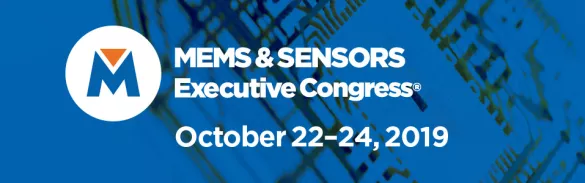
MEMS and Sensors Executive Congress 2019
Register for this year's MEMS & Sensors Executive Congress, October 22-24, 2019 in Coronado, California, USA. This year will see a different format to truly focus on the needs of the decision making executives in our industry. Industry economic and business updates will be covered from different aspects of the ecosystem together with forward-looking strategic and technology trends.
Jérôme Azemar, Yole Développement will be speaking during Session 3: Markets, Applications and Technology Trends.
Register before September 20, 2019 for Early Bird Pricing!
As Project Development Director at Yole Développement (Yole), Jérôme Azémar is supporting the development of strategic projects, following leading customers of the company within the semiconductor industry, from manufacturing to packaging. His mission is to develop Yole’s business and technical knowledge in the industry, maintain long term relationships with its accounts and meet their expectations.
Jérôme is a member of Yole since 2013 and worked as a senior analyst, managing the day to day production of technology & market reports as well as custom consulting projects. He also deeply contributed to the business development of the Advanced Packaging & Semiconductor Manufacturing activities.
Jérôme is the author of numerous analysis and international publications covering advanced packaging, power electronics and semiconductor manufacturing. He is also regularly involved in international conferences, giving presentations, delivering keynotes, as well as organizing committees.
Along his career, Jérôme has developed a large network in the industry, being in touch with CEOs, CTOs, Marketing Managers, Business Development Managers…
Prior to this and upon graduating from INSA Toulouse (France) with a Master’s in Microelectronics and Applied Physics, Jérôme joined ASML and worked in Veldhoven (The Netherlands) for three years as an Application Support Engineer specializing in immersion scanners. During this time, he acquired Photolithography skills which he then honed over a two-year stint as a Process Engineer at STMicroelectronics (France).
Despite a 2018 year when both automotive and consumer markets have stagnated, the MEMS market did not recess compared to 2017. Its market value reached $11.6B in 2018, with consumer applications accounting for more than 60% of the total market. The MEMS market will experience +8.3% annual growth in value driven by pressure (for TPMS), RF (for V2X 5G communications), inertial (for ADAS) and future MEMS (such as pMUT for ultrasonic fingerprint).
Additionally, sensor fusion is becoming more and more relevant since many billion MEMS sensors are made per year. The upcoming 5G revolution will make connectivity easier than ever, creating exponentially more data. This leads to “Big data”, an industry born of recent advancements in AI and machine learning, built upon and fueled by a wealth of new data from ever-expanding sensor applications. An upcoming trend is edge computing, with sensors and MEMS driving a new age of technology. Sensors are digitizing the human experience, and as the real and virtual worlds move closer together, it will be sensors that bind them, enabling new experiences for users everywhere. Running AI at the edge, coupled with sensor fusion, will open new applications for MEMS in audio, motion, olfactometry, and imaging.
MSIG Webinar: An Exciting Glimpse into the Future of MEMS
8:00 am - 8:30 am
Off
Add to Calendar2019-10-03 08:00:002019-10-03 08:30:00MSIG Webinar: An Exciting Glimpse into the Future of MEMSA MEMS and Sensors Industry Group Hosted Webinar
Despite a 2018 year when both automotive and consumer markets have stagnated, the MEMS market did not recess compared to 2017. Its market value reached $11.6B in 2018, with consumer applications accounting for more than 60% of the total market. The MEMS market will experience +8.3% annual growth in value driven by pressure (for TPMS), RF (for V2X 5G communications), inertial (for ADAS) and future MEMS (such as pMUT for ultrasonic fingerprint).
Additionally, sensor fusion is becoming more and more relevant since many billion MEMS sensors are made per year. The upcoming 5G revolution will make connectivity easier than ever, creating exponentially more data. This leads to “Big data”, an industry born of recent advancements in AI and machine learning, built upon and fueled by a wealth of new data from ever-expanding sensor applications. An upcoming trend is edge computing, with sensors and MEMS driving a new age of technology. Sensors are digitizing the human experience, and as the real and virtual worlds move closer together, it will be sensors that bind them, enabling new experiences for users everywhere. Running AI at the edge, coupled with sensor fusion, will open new applications for MEMS in audio, motion, olfactometry, and imaging.United StatesSEMI.org[email protected]America/Los_Angelespublic
America/Los_Angeles
FOA Members only, for details contact the FOA Team - [email protected].
Off
Add to Calendar2020-02-19 00:00:002020-02-20 00:00:00FOA Q1 2020 Collaborative ForumFOA Members only, for details contact the FOA Team - [email protected].Embassy Suites by Hilton Scottsdale Resort 5001 N. Scottsdale Road Scottsdale, AZ 85250 United StatesSEMI.org[email protected]America/Los_Angelespublic
America/Los_Angeles
Analog Devices - Who We Are Our customers are at the center of our identity, and we are endlessly committed to their success. We listen to our customers and anticipate their needs, working with and alongside them to reduce complexity and co-create the innovations that disrupt markets and help solve the world’s most pressing challenges. Whether discussing the role of technology in helping to mitigate global sustainability concerns or rolling up our sleeves and designing solutions at the Intelligent Edge, ADI has the industry and technology expertise to help our customers succeed.
Analog Devices 14320 SW Jenkins Rd Beaverton, OR97005 United States
July 29, 2025 - Day 1: Women's Breakfast/Discussion & Social Activity, Golf Event, & Networking Reception
8:00 am
-
11:00 am
Women in FOA -Breakfast (Analog Devices)/Discussion & Social Activity
Meeting room: Washington Park
11:00 am
-
5:00 pm
FOA Golf Event - The Reserve Vineyards & Golf Club
Address:
4805 SW 229th Ave
Aloha, OR 97007
6:00 pm
-
9:00 pm
Welcome Reception - The Reserve Vineyards & Golf Club
Address:
4805 SW 229th Ave
Aloha, OR 97007
July 30, 2025 - Day 2: Full Membership Meeting, Fab Tour & Networking Event
8:00 am
-
12:30 pm
Device Maker Morning Meeting, Fab Tour & Feed Back Session - Analog Devices
Meeting Room: Washington Park
10:00 am
-
12:30 pm
Solution Provider Morning Meeting - Analog Devices
Meeting room: Beaverton Cafe
12:30 pm
-
2:00 pm
Lunch
All FOA members: Analog Devices
Lunch to be held in: Beaverton Cafe
2:00 pm
-
6:00 pm
Full Membership Meeting - Analog Devices
Meeting room: Beaverton Cafe
4:00 pm
-
6:00 pm
Fab Tour
Fab Tour - Murel and Robotics Upskilling Lab
7:00 pm
-
10:00 pm
Evening Social Event - KingPins - Beaverton
Address:
2725 SW Cedar Hills Blvd
Beaverton, OR 97005 United States
Major investments are developing in semiconductor fab capacity expansion globally and North America. Join industry colleagues online Friday, October 22, for a thought-provoking, VIRTUAL forum on the outlook, competitive environment, market, and technology trends driving fab expansion investment in the semiconductor industry. The discussion includes an analysis of the opportunities and challenges presented by end market drivers.
Hear our panel of industry and Wall Street experts discuss the latest technology trends, the global competitive environment, and the decision-making process for regional and state-level investments. Topics include:
Market and Technology Trends Driving New Investment
Emerging Technologies, Integration Schemes, and Manufacturing Processes
Economic, Geopolitical, and the Global Competitive Environment (includes US-China Tensions)
Factors that Influence Global and State-Level Decisions on Where Fab Investment Occurs
Venture Capitalism in the Industry and Growth Trends
Semiconductor Chip Shortage
And more
Explore industry trends from the economic, market, technology, and manufacturing perspectives, plus valuable information from the viewpoint of each speaker.
Virtual Event, Pacific Time United States
Friday, October 22, 2021
8:30 am
-
8:35 am
Janell Centers
Marketing Manager, Semiconductor and Technology
Macquarie Electronics
Welcome, Introduction
8:35 am
-
9:00 am
Charles Shi, PhD
Vice President & Research Analyst, Semiconductor Capital Equipment
Needham & Company
KEYNOTE—The War for Semiconductor Process and Packaging Leadership in the Era of a Slowing Moore’s Law
For more information on sponsorship, please contact Eric Rude - [email protected]
In addition to presentations from recognized thought leaders for each smart manufacturing Topic, there will be breakout sessions which will enable individuals to further explore use cases with subject-matter-experts. Workshop topics include:
How to use ROI to select Smart Manufacturing solutions. Leverage data access, communications protocols and data sharing practices to enable new applications?
Compare and contrast common solutions for data flow architectures and material handling for improving cycle time and yield.
Best practices for Data Security Audits and cyber-attack prevention.
Where is machine-learning and artificial intelligence best used to improve overall productivity and automation?
SEMI Global Headquarters 673 S. Milpitas Blvd Milpitas, CA95035 United States
Wednesday, September 11
5:30 pm
-
7:30 pm
Evening Reception
Rockwell Automation Electric Vehicle (EV) Innovation Center
111 N. Market Street, San Jose, CA 95113
SEMI’s Smart Manufacturing Technology Community invites you to a one-day workshop to discuss solutions to critical issues to realize the benefits of smart manufacturing across the Semi/OSAT/PCBA segments of the electronic manufacturing supply chain. Walk away with ideas on how to maximize the impact of smart manufacturing solutions deployed across the electronics manufacturing industry and opportunities for collaboration across the supply chain using smart manufacturing principles.
Smart Manufacturing Workshop: Successful Implementation and Opportunities for Enabling Technologies
8:00 am - 5:00 pm
Off
Add to Calendar2019-09-12 08:00:002019-09-12 17:00:00Smart Manufacturing Workshop: Successful Implementation and Opportunities for Enabling TechnologiesA SEMI Smart Manufacturing Workshop
SEMI’s Smart Manufacturing Technology Community invites you to a one-day workshop to discuss solutions to critical issues to realize the benefits of smart manufacturing across the Semi/OSAT/PCBA segments of the electronic manufacturing supply chain. Walk away with ideas on how to maximize the impact of smart manufacturing solutions deployed across the electronics manufacturing industry and opportunities for collaboration across the supply chain using smart manufacturing principles.SEMI Global Headquarters 673 S. Milpitas Blvd Milpitas, CA 95035 United StatesSEMI.org[email protected]America/Los_Angelespublic
America/Los_Angeles
MSIG Webinar - The MEMS Market Labyrinth: What You Need to Know
MEMS, imaging and sensors devices are driving innovation and causing demand to explode in transportation, medical, mobile, industrial and other Internet of Things (IoT) applications, which are all focus areas of this year SEMI MEMS & Imaging Sensors Summit, 25 to 27 September 2019 in Grenoble, France.
This webinar will present a current view of the MEMS technology competitive landscape, the role of MEMS and Sensors big industry players and the struggle for differentiation to dominate the market.
The session will provide a deep dive into MEMS market trends, challenges and opportunities and will also highlight results from Yole Développement´s recently released outlook.
United States
8:00 am
-
8:15 am
Introduction
8:15 am
-
8:45 am
Dimitrios Damianos
Technology Market Analyst, Yole Développement
The next turn will take us out of the MEMS labyrinth or further inside?
Abstract
In a gloomy economic environment, the MEMS industry is holding up. Following the semiconductor industry, MEMS had its best year so far, but with a slower YoY growth than expected. Consumer and automotive are responsible for almost 80% of the $11.5B market in 2018, driven mainly by inertial, pressure, microphone, infrared, RF and optical MEMS. Big players are competing in their corresponding established markets, eating up each other’s share of the pie. Competition therefore is getting fierce with each player struggling for differentiation in order to dominate the market. Piezoelectric tech, sensor fusion, AI & edge computing take the MEMS industry by hand up to the next corner of the market labyrinth. Will they lead it out to new horizons and further growth? Join the webcast regarding the status of the MEMS industry to find out!
Biography
Dimitrios Damianos, PhD joined Yole Développement (Yole) as a Technology and Market Analyst and is working within the Photonics, Sensing & Display division. Dimitrios is daily working with his team to deliver valuable technology & market reports regarding the imaging industry including photonics & sensors. After his research on theoretical and experimental quantum optics and laser light generation, Dimitrios pursued a Ph.D. in optical and electrical characterization of dielectric materials on silicon with applications in photovoltaics and image sensors, as well as SOI for microelectronics at Grenoble’s university (France). In addition, Dimitrios holds a MSc degree in Photonics from the University of Patras (Greece). He has also authored and co-authored several scientific papers in international peer-reviewed journals.
MSIG Webinar - The MEMS Market Labyrinth: What You Need to Know
8:00 am - 9:00 am
Off
Add to Calendar2019-09-05 08:00:002019-09-05 09:00:00MSIG Webinar - The MEMS Market Labyrinth: What You Need to KnowA SEMI-MSIG | Yole Developpement Hosted WebinarUnited StatesSEMI.org[email protected]America/Los_Angelespublic
America/Los_Angeles