MILPITAS, Calif. — February 5, 2024 — SEMI today announced the availability of a free quick start guide to facilitate the onshoring of advanced packaging facilities in the United States and support the region’s buildout of a semiconductor manufacturing supply chain. Offered by SEMI and the UCLA Center for Heterogeneous Integration and Performance Scaling (CHIPS) and funded by the National Institute of Standards and Technology (NIST), the Manufacturing Roadmap for Heterogeneous Integration and Electronics Packaging (MRHIEP) highlights critical areas of development needed to establish advanced packaging facilities on U.S. soil.
 Based on the Heterogeneous Integration Roadmap (HIR), the guide incorporates a manufacturing approach to implement the HIR. Some 100 chip industry veterans from more than 40 companies collaborated with representatives from academic institutions, industrial consortia, and government agencies to develop the guide.
Addressing hardware and software tools, manufacturing processes, and supplier infrastructure, the guide covers tools, processes, standards, and interdependencies that enable advanced packaging for high-performance computing (HPC), medical, health and wearables applications.
“The MRHIEP drills down into operational objectives by examining current capabilities and highlighting critical areas of development needed for onshored manufacturing to be successful in the U.S.,” said Melissa Grupen-Shemansky, SEMI CTO. “The guide provides vital support for implementation of the HIR, a comprehensive document addressing the global supply chain for heterogenous integration.”
Download the guide.
About SEMI
SEMI® is the global industry association connecting over 3,000 member companies and 1.5 million professionals worldwide across the semiconductor and electronics design and manufacturing supply chain. We accelerate member collaboration on solutions to top industry challenges through Advocacy, Workforce Development, Sustainability, Supply Chain Management and other programs. Our SEMICON® expositions and events, technology communities, standards and market intelligence help advance our members’ business growth and innovations in design, devices, equipment, materials, services and software, enabling smarter, faster, more secure electronics. Visit www.semi.org, contact a regional office, and connect with SEMI on LinkedIn and X to learn more.
Association Contact
Michael Hall/SEMI US
Phone: 1.408.943.7988
Email: [email protected]

 Themed Innovation Beyond Boundaries, SEMICON Korea 2024 is expected to draw record attendance of 70,000 as 500 companies showcase the latest semiconductor manufacturing technologies. The event will host 30 technology and business conferences featuring more than 200 visionaries and experts as speakers. Opportunities for companies from across the semiconductor supply chain to connect and explore new collaborations will also be a key feature.







 The European Commission designed the European Economic Security Strategy to protect the European Union’s economic security and reinforce the resilience of its economy by investing in the region’s competitiveness, diversifying its supply chains, and minimizing the risks of economic interdependencies.
 Themed Key Strategies for Europe’s Success: An Evolving Global Landscape, ISS Europe 2024 will examine economic, technology, market, business, and societal developments and trends influencing the global electronics manufacturing industry.
  “Electronic design automation (EDA) reported record revenue growth in Q3 23,” said Walden C. Rhines, Executive Sponsor of the SEMI Electronic Design Market Data report. “This was the highest overall growth since Q4 1998. The Computer-Aided Engineering, IC Physical Design and Verification, Printed Circuit Board and Multi-Chip Module, and Semiconductor Intellectual Property categories reported double-digit growth. Further, all geographic regions reported substantial growth.”
 Themed Ready, Set and Ramp?, the event at the Ritz-Carlton in Half Moon Bay, Calif. will present industry intelligence to help inform company business plans and forecasts based on current market conditions.
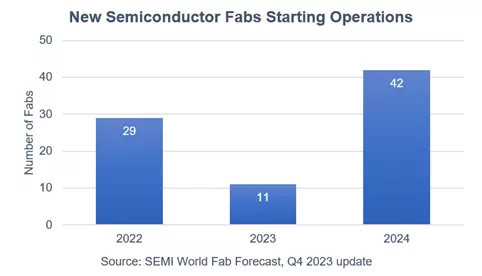
 The 2024 growth will be driven by capacity increases in leading-edge logic and foundry, applications including generative AI and high-performance computing (HPC), and the recovery in end-demand for chips. The capacity expansion slowed in 2023 due to softening semiconductor market demand and the resulting inventory correction.