
MILPITAS, Calif. ─ April 11, 2024 ─ SEMI, the industry association serving the global electronics design and manufacturing supply chain, today issued the following statement from Ajit Manocha, SEMI President and CEO, after the United States government announced it will no longer move forward with the Notice of Funding Opportunity for CHIPS funding for the construction, modernization, or expansion of semiconductor research and development (R&D) facilities in the United States:
 “We recognize that the Department of Commerce was faced with a difficult decision to change course regarding the issuance of a third Notice of Funding Opportunity related to R&D under the CHIPS and Science Act due to recent legislative actions directing the department to make a $3.5 billion investment in secure enclave. While we acknowledge the importance of the underlying objectives guiding recent decisions, we are concerned about their impact on longstanding plans for implementing the CHIPS Act, which was shaped by extensive stakeholder input and industry analysis.”
“Strong investment and support for R&D is essential to advance foundational technologies across the semiconductor supply chain and enhance the overall competitiveness of the U.S. semiconductor industry. Private R&D is the cornerstone of the semiconductor industry, propelling the next generation of innovation. SEMI urges Congress to work alongside the Department of Commerce to fulfill the intent of the CHIPS and Science Act of 2022 to fund private R&D activities under the legislation. Key investments to spur and scale private R&D projects must be paired with support for the National Semiconductor Technology Center (NSTC) to meet the objectives of CHIPS and Science Act and secure the United States’ technological leadership. SEMI stands ready to work with the Department of Commerce and Congress to ensure robust funding for private R&D projects.”
Visit SEMI Global Advocacy to learn more about public policy efforts and developments, and SEMI Workforce Development for more information on efforts to address the microelectronics industry’s talent needs.
About SEMI
SEMI® is the global industry association connecting over 3,000 member companies and 1.5 million professionals worldwide across the semiconductor and electronics design and manufacturing supply chain. We accelerate member collaboration on solutions to top industry challenges through Advocacy, Workforce Development, Sustainability, Supply Chain Management and other programs. Our SEMICON® expositions and events, technology communities, standards and market intelligence help advance our members’ business growth and innovations in design, devices, equipment, materials, services and software, enabling smarter, faster, more secure electronics. Visit www.semi.org, contact a regional office, and connect with SEMI on LinkedIn and X to learn more.
Association Contacts
Samer Bahou/SEMI US
Phone: 1.408.943.7870
Email: [email protected]
Michael Hall/SEMI
Phone: 1.408.943.7988
Email: [email protected]
 The initial in-person trainings will be held at SEMI headquarters in Milpitas, California. See the
  Themed Heterogeneous Systems for the Intelligently Connected Era, this year’s SEMI 3D & Systems Summit will feature a broader scope of topics including market trends, chiplet design, hybrid bonding, Co-Packaged Optics (CPO), high-bandwidth computing and environmental sustainability.
 Featuring keynotes by thought leaders from IBM, Wolfspeed, and Semiconductor Advisors, ASMC 2024 is the premier event where industry professionals network and share insights into best practices for semiconductor manufacturing. The conference is co-chaired by Bradley Wood, Applications Engineering Manager, CMP Filtration at Entegris, and Vijayalakshmi Seshachalam, CVD Process Engineer Lead at GlobalFoundries.
 Worldwide 300mm fab equipment investment is expected to increase 20% to US$116.5 billion in 2025 and 12% to US$130.5 billion in 2026 before hitting a record high in 2027.
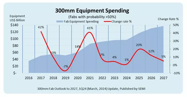
 Themed Sensorizing Our World: Technology Driving Global Solutions, MSTC 2024 will feature keynotes and technical sessions on critical MEMS and sensors topics. Highlights also include posters showcasing novel applications from the next generation of innovators and networking opportunities for participants to help grow their businesses.


 Themed Boosting Agility and Resiliency of the Global Electronics Supply Chain, SEMICON Southeast Asia 2024 will feature more than 500 exhibiting companies and more than 1,000 booths, doubling participation from last year’s exhibition and conference. The exponential expansion underscores the rising interest in Southeast Asia's semiconductor sector and the increasing importance of SEMICON Southeast Asia, the region’s premier global electronics manufacturing and supply chain event, in bringing industry stakeholders together to pursue new innovation and growth opportunities.