downloadGroupGroupnoun_press release_995423_000000 copyGroupnoun_Feed_96767_000000Group 19noun_pictures_1817522_000000Member company iconResource item iconStore item iconGroup 19Group 19noun_Photo_2085192_000000 Copynoun_presentation_2096081_000000Group 19Group Copy 7noun_webinar_692730_000000Path
Skip to main content
Default Banner Image

Taiwan

Semiconductor equipment manufacturer ClassOne Technology announced the sale of its Solstice® S8 electroplating system to a major semiconductor foundry service based in Taiwan. This is the second S8 to be purchased by the company. The 8-chambered Solstice platform is designed specifically for ≤200mm wafer processing. The new tool will be used to produce Heterojunction Bipolar Transistors (HBTs) and Vertical Cavity Surface Emitting Lasers (VCSELs). The announcement was made by ClassOne’s CEO, Byron Exarcos, and Senior Technology Director, John Ghekiere.

“This user is a high-volume semiconductor manufacturer,” said Ghekiere. "So they are interested not only in the Solstice's superior plating performance, but also in its reliable, fully-automated high throughput. The tool is being used for wafer level packaging processes, including copper pillar and solder bump electroplating.”

“This customer has been using our Solstice S8 electroplating equipment for several years now," said Exarcos. “The tool has been fully qualified for their processes and is meeting their aggressive performance goals. Now, their business is rapidly expanding, and they've chosen to bring in a second S8 to support that growth. We're actually seeing this pattern across the industry today. As Solstice is becoming embedded into customer processes, the repeat orders are coming in with increased frequency. We're very gratified by this vote of confidence in the Solstice and in ClassOne.”

Ghekiere noted that today’s HBT devices are used in many ultrafast circuits and those requiring high power efficiency, including next-generation RF power amplifiers, 5G cellular phones, etc. VCSELs are used in 2D and 3D imaging, facial recognition, smart-glasses, fiber optic communications, LiDAR, and much more.

The ClassOne Solstice S8 is an 8-chamber system for high-performance, fully-automated electroplating and surface preparation. The Solstice series, which was specifically designed for ≤200mm wafer processing, also includes the S4, which provides up to four processing chambers, and the LT, with up to three chambers. In addition to electroplating, the tool’s special Plating-Plus™ capabilities enable it to handle a number of other surface preparation functions, including wafer cleaning, high-pressure metal lift-off, resist strip, UBM etch and more. This multi-processing flexibility serves to streamline process production and can reduce the number of different tools a user needs to purchase.

About ClassOne Technology
ClassOne Technology (classone.com) provides innovative wet-chemical equipment solutions, including electroplaters, spin-rinse-dryers, spray solvent tools and more. The company focuses on making advanced processing technology available to users of ≤200mm wafers, such as compound semiconductor and many emerging markets, who traditionally have been underserved by the larger equipment manufacturers. ClassOne Technology’s equipment has become known for its unique combination of advanced performance, flexibility and cost-efficiency Based in Kalispell, Montana, ClassOne Technology is built upon decades of experience from industry veterans creating high-performance semiconductor equipment. ClassOne Technology is a sister company to ClassOne Equipment (ClassOneEquipment.com), the industry’s premier provider of refurbished name-brand processing tools, with over 2,500 systems installed worldwide.

For more information, contact:
Byron Exarcos
ClassOne Technology
109 Cooperative Way
Kalispell, MT 59901
tel: +1 (678) 772-9086
email: [email protected]

Taiwan
Highlighted content

Zhubei City, Hsinchu County
Taiwan

Standards

Jan. 7, 2021

Time: 1:00-3:00 PM

Venue: SEMI Taiwan Office, Zhubei City, Hsinchu County, Taiwan.

Standards Contact Information:

Cher Wu 吳琇君

Senior Executive Consultant | Standards

SEMI Taiwan

+886-933-976766

[email protected]

1:00 pm - 3:00 pm Off Add to Calendar 2021-01-07 13:00:00 2021-01-07 15:00:00 I&C Taiwan TC Chapter meeting Jan. 7, 2021 Time: 1:00-3:00 PM Venue: SEMI Taiwan Office, Zhubei City, Hsinchu County, Taiwan. Agenda_20210107_I_C Taiwan TC Chapter Meeting_Hybrid.pdf (293.69 KB) Standards Contact Information: Cher Wu 吳琇君 Senior Executive Consultant | Standards SEMI Taiwan +886-933-976766 [email protected] Zhubei City, Hsinchu County Taiwan SEMI.org [email protected] Asia/Taipei public Asia/Taipei

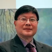
FREMONT, Calif. – Dec 7, 2020 – YES (Yield Engineering Systems, Inc.), a leading manufacturer of process equipment for semiconductor advanced packaging, life sciences and AR/VR applications, today announced that Alex Chow has joined the company as Asia Sales President and General Manager.

To his new role, Mr. Chow brings 20 years of executive positions at Onto Innovation and Ultratech, and many successful strategic partnerships with top-tier IDMs, foundries and OSATs. He will be responsible for growing the company’s presence in the APAC region by working with existing partners as well as by growing YES’s direct Asia presence. One of his initial actions will be to open a YES Asia office in Hsinchu, Taiwan to support the vibrant Taiwanese Advanced Packaging market.

“We see great potential for YES products in the APAC region,” said Rezwan Lateef, President of YES. “Alex comes to YES with a strong record of driving product and business growth in Asia and elsewhere. We expect that his experience in building relationships with the world’s largest semiconductor companies will be of particular value to us as we expand our position in the region.”

Mr. Chow came to YES from Onto Innovation, where he was Vice President of Advanced Packaging Solutions. Before that, he was Vice President of Product Marketing at Ultratech, Inc. His career began at Suss Microtec, where he was a senior applications engineer. Mr. Chow holds a master’s degree in Materials Science and Engineering from the University of Maryland, College Park and has completed the Executive Education program in Strategy in Competitive Markets at the University of California, Berkeley.

About YES
YES (Yield Engineering Systems, Inc.) is a leading manufacturer of high-tech, cost-effective equipment for transforming surfaces, materials and interfaces. The company’s product lines include vacuum cure ovens, chemical vapor deposition (CVD) systems, and plasma etching tools used for precise surface modification and thin-film coating of semiconductor wafers, semiconductor and MEMS devices, and biodevices. With YES, customers ranging from startups to Fortune 100 companies can create and volume-produce products in a wide range of markets, including Advanced Packaging, MEMS, Augmented Reality/Virtual Reality and Life Sciences. YES is headquartered in Fremont, California, with a growing global presence. For more information, please visit www.yieldengineering.com.

ST. PETERSBURG, Fla. (Dec. 3, 2020) — Plasma-Therm, a leading manufacturer of plasma-process equipment for the semiconductor industry, announced today the acquisition of OEM Group’s dry process equipment business.

With the acquisition, Plasma-Therm has acquired all original OEM licenses and intellectual property rights for SFI Endeavor, AG Heatpulse, MRC Eclipse, and Tegal brand equipment. Plasma-Therm will continue to support existing customers through spare parts and upgrades, while offering new and refurbished tools to the wider market.

“The acquisition allows Plasma-Therm’s award-winning customer service teams to support the large and global install base,” said Abdul Lateef, CEO of Plasma-Therm. “Additionally, PVD and RTP technologies align perfectly with our etch and deposition products and process solutions, which will further support the manufacturing and R&D needs and requirements of our customers.”

Michael Correra, CEO of OEM Group, said, “We are delighted to have had these outstanding products acquired by Plasma-Therm, ensuring a strong path to market for our newly developed Endeavor M series PVD platform, and the continued availability and support of the MRC Eclipse, AG Heatpulse, and Tegal products. This acquisition allows OEM Group to strategically focus on our wet chemical process and ion implant technologies.”

About Plasma-Therm
Established in 1974, Plasma-Therm is a manufacturer of advanced plasma processing equipment for specialty semiconductor markets, including advanced packaging, wireless communication, photonics, solid-state lighting, MEMS/NEMS, nanotechnology, renewable energy, data storage, photomask, and R&D. Plasma-Therm offers leading etch and deposition technologies and solutions for these markets. Sales and service locations throughout North America, Europe, and Asia-Pacific meet the diverse needs of Plasma-Therm’s global customer base. Visit www.plasmatherm.com for more information.

About OEM Group
Established in 1999, OEM Group is a semiconductor capital equipment manufacturer and innovator in new and remanufactured 75mm – 300mm tools, spare parts, upgrades, and services. We serve the LED, MEMS, Wireless, Power, Energy Harvesting, WLP, Data Storage, and Logic markets. OEM Group's current portfolio of products includes the Semitool & Cintillio Spray Ozone Tool, Spray Acid Tool, and Spray Solvent Tool, Spin Rinse Dryer and Storm, Varian Implant, and AMAT P5000 CVD & Etch.

ESPOO, Finland, 2nd December 2020 – Picosun Group, leading provider of AGILE ALD® (Atomic Layer Deposition) thin film coating solutions for industrial manufacturing, presents PicoOS™, the new, full stack operating system and process control software for PICOSUN® ALD equipment.

“PicoOS™ brings PICOSUN® ALD equipment control to the modern era. It is designed for wafer fabs and industrial environments where transition to Industry 4.0 is ongoing. Data-driven PicoOS™ enables future production solutions where machine learning, artificial intelligence, internet-of-things, and other new digital inventions are utilized for optimum industrial efficiency,” says Dr. Jani Kivioja, CTO of Picosun Group.

Picosun’s proprietary PicoOS™ software combines individual ALD module, wafer handling and transfer system, and instrumentation control under one common graphical HMI (human-machine interface). This ensures easy, intuitive and user-friendly operation, maintenance, and configuration of the whole PICOSUN® ALD cluster.

PicoOS™ enables full factory integration via SECS/GEM protocol, process and system data logging down to 20 ms rate, and real-time export of all data for continuous monitoring and further analysis.

PicoOS™ operating system is specifically developed by Picosun’s own in-house software team for the company’s fully automated production ALD systems Morpher and Sprinter, and it will be implemented in all future PICOSUN® ALD tool platforms.

“PicoOS™ is designed to ensure the highest control precision and accuracy, the fastest service times, and the best user experience for our customers. Having in-house control over all features and sub-components of our PICOSUN® ALD solutions is a key part of our holistic service model,” continues Kivioja.

PicoOS™ has freely configurable and scalable editor for ALD process recipe and processing job creation and storage, and recipes can be edited or new ones created any time during the ALD system operation. Configurable user levels and safety logic, instrumentation and interlocks guarantee safe use in day-to-day operations, and allow full access for tool management in maintenance situations. Maintenance procedures are sped up by specific clean-up and maintenance sequences inbuilt in the software.

About Picosun
Picosun provides the most advanced AGILE ALD® (Atomic Layer Deposition) thin film coating solutions for global industries. Picosun’s ALD solutions enable technological leap into the future, with turn-key production processes and unmatched, pioneering expertise in the field – dating back to the invention of the technology itself. Today, PICOSUN® ALD equipment are in daily manufacturing use in numerous leading industries around the world. Picosun is based in Finland, with subsidiaries in Germany, USA, Singapore, Japan, South Korea, China mainland and Taiwan, offices in India and France, and a world-wide sales and support network. Visit www.picosun.com.

More information:
Dr. Jani Kivioja
CTO, Picosun Group
Tel: +358 50 321 1955
Email: [email protected]
Web: www.picosun.com

ESPOO, Finland, 2nd December 2020 – Picosun Group, the leading supplier of AGILE ALD® (Atomic Layer Deposition) thin film coating solutions for global industries, has launched Sprinter, a brand new, fully automated high throughput ALD production module for 300 mm wafers. Barrier, high-k and other films are deposited in Sprinter with perfect ALD for semiconductor (e.g. emerging memory, transistor, capacitor), display, and IoT component applications.

In Sprinter, single wafer film quality and uniformity are upscaled to fast batch processing with the highest reliability and repeatability(*).

Compared to vertical furnace reactors typically used for batch ALD processing, Sprinter provides higher film quality with lower thermal budget, so it is suitable also for temperature-sensitive devices.

Sprinter combines very fast process times with smaller batch sizes than in vertical furnaces, which allows greater production flexibility and minimized risk without sacrificing throughput.

The core of the Sprinter is its disruptively designed reaction chamber, where fully laminar precursor flows ensure perfect ALD deposition with no parasitic CVD growth. This minimizes the need for system maintenance.

“PICOSUN® Sprinter meets directly the challenges in high volume ALD manufacturing on 300 mm wafers. We are happy to unveil this product to our new and existing customers in 300 mm semiconductor markets, and offer them a truly disruptive, modern alternative to old technologies in batch ALD manufacturing,” says Mr. Jussi Rautee, CEO of Picosun Group.

SEMI S2/S8 certified PICOSUN® Sprinter module can be integrated to customer’s manufacturing line or cluster. It is suitable also for single wafer manufacturing lines as it does not disturb the process flow. Sprinter is run with Picosun’s new, proprietary PicoOS™ operating system and process control software.

“Together with Sprinter, we are launching also our PicoOS™ operating system. Own operating system and process control software, developed by our in-house software team, means the highest control precision and accuracy, the fastest service times, and the best reliability and quality for our customers,” continues Rautee.

Full stack PicoOS™ software allows control, operation and configuration of PICOSUN® ALD equipment – either standalone systems or full production clusters – via one unified, intuitive, and user-friendly graphical HMI and ensures smooth connection between the system and the customer’s factory automation via SECS/GEM protocol.

Sprinter is available for process demos at Picosun facilities. Sprinter module sales starts in January 2021 and full Sprinter cluster with several ALD modules, central vacuum wafer handling unit and EFEM is available later in spring 2021.

(*)PICOSUN® Sprinter ALD batch process data on 300 mm Si wafers, Al2O3 process as an example (more data available on request):

Parameter Value
Film thickness 1σ non-uniformity, within-wafer @ 200 oC About Picosun
Picosun provides the most advanced AGILE ALD® (Atomic Layer Deposition) thin film coating solutions for global industries. Picosun’s ALD solutions enable technological leap into the future, with turn-key production processes and unmatched, pioneering expertise in the field – dating back to the invention of the technology itself. Today, PICOSUN® ALD equipment are in daily manufacturing use in numerous leading industries around the world. Picosun is based in Finland, with subsidiaries in Germany, USA, Singapore, Japan, South Korea, China mainland and Taiwan, offices in India and France, and a world-wide sales and support network. Visit www.picosun.com.

More information:
Mr. Jussi Rautee
CEO, Picosun Group
Tel: +358 50 345 4457
Email: [email protected]
Web: www.picosun.com

Taiwan Standards
Highlighted content

East District, Hsinchu City
Taiwan

Standards

Automation Technology Taiwan TC Chapter                                            

Committee TC meeting

Friday, December 25, 2020

5F No. 69 Minzu Road, East District, Hsinchu City

14:00–16:00

Agenda:


Standards Contact Information

Cher Wu 吳琇君

Senior Executive Consultant | Standards

SEMI Taiwan

+886-933-976766

[email protected]

2:00 pm - 4:00 pm Off Add to Calendar 2020-12-25 14:00:00 2020-12-25 16:00:00 Automation Technology Taiwan TC Chapter Meeting Automation Technology Taiwan TC Chapter                                             Committee TC meeting Friday, December 25, 2020 5F No. 69 Minzu Road, East District, Hsinchu City 14:00–16:00 Agenda: Agenda_20201225_Automation Technology Taiwan TC Chapter Meeting.pdf (240.55 KB)   Standards Contact Information Cher Wu 吳琇君 Senior Executive Consultant | Standards SEMI Taiwan +886-933-976766 [email protected] East District, Hsinchu City Taiwan SEMI.org [email protected] Asia/Taipei public Asia/Taipei
Taiwan Standards
Highlighted content

East District, Hsinchu City
Taiwan

Standards

Photovoltaic Taiwan TC Chapter Meeting

Friday, December 25, 2020

5F No. 69 Minzu Road, East District, Hsinchu City

10:00 – 12:00


Agenda:


Standards Contact Information

Cher Wu 吳琇君

Senior Executive Consultant | Standards

SEMI Taiwan

+886-933-976766

[email protected]

10:00 am - 12:00 pm Off Add to Calendar 2020-12-25 10:00:00 2020-12-25 12:00:00 Photovoltaic Taiwan TC Chapter Meeting Photovoltaic Taiwan TC Chapter Meeting Friday, December 25, 2020 5F No. 69 Minzu Road, East District, Hsinchu City 10:00 – 12:00   Agenda: Agenda_20201225_PV Taiwan TC Chapter Meeting.pdf (116.91 KB)   Standards Contact Information Cher Wu 吳琇君 Senior Executive Consultant | Standards SEMI Taiwan +886-933-976766 [email protected] East District, Hsinchu City Taiwan SEMI.org [email protected] Asia/Taipei public Asia/Taipei

ESPOO, Finland, 23rd November 2020 – Picosun Group, the leading supplier of AGILE ALD® (Atomic Layer Deposition) thin film coating solutions, partners with prominent Chinese hospitals and researchers to apply medical ALD technology for safer surgical procedures.

Picosun’s biocompatible ALD coatings will be applied on electrosurgical equipment (electrotomes) to improve their performance, safety, and service life.

“It’s great to collaborate with a company such as Picosun to develop solutions for safer and more patient-friendly surgeries. Picosun is the leader in medical ALD solutions. The company has extensive process portfolio for biocompatible ALD materials and their equipment are at use at several medical equipment manufacturers around the world. In China, Picosun is the market leader with numerous PICOSUN® ALD systems installed throughout the country. We have strong trust that this collaboration will result in disruptive new innovations and novel solutions for surgical equipment,” says Longsheng Lu, Professor of South China University of Technology.

Electrotome utilizes high temperature to cut and separate tissue, with simultaneously coagulating blood, and it’s a standard equipment replacing traditional mechanical scalpels in many operations. Tissue and blood sticking and burning on the electrotome blade is a serious problem because the crusted blade risks increased bleeding, tissue damage, tearing and scarring, thus making the patient’s healing time longer. Smoke from the burning tissue may also hinder the surgeon’s vision and increase the risk for error during delicate procedures such as cardiac or neurosurgery.

This far, there hasn’t been a working solution in the market to overcome this problem. ALD technology can potentially provide this solution and thus improve patient safety, wound quality and healing time. ALD forms ultra-thin, pinhole-free coatings with unmatched conformality over the smallest microscale details of the surface, and the ALD process can be performed at moderate temperatures so the method is suitable also for sensitive materials. Deposited over special anti-adhesive micropatterning of the electrotome blade, biocompatible ALD film prevents blood and tissue from sticking to the blade.

“We are happy to extend our PicoMEDICAL™ technology to a yet new healthcare application, and to work with top tier Chinese hospitals and scientists to qualify our solutions in everyday use. ALD is revolutionizing the medical field right now, just like it did to semiconductor industries over a decade ago. We at Picosun want to use our extensive ALD know-how to develop solutions to improve people’s health and quality of life, which is why medical ALD is one of our key markets for the future,” continues Dr. Jani Kivioja, CTO of Picosun Group.

Picosun provides the most advanced AGILE ALD® (Atomic Layer Deposition) thin film coating solutions for global industries. Picosun’s ALD solutions enable technological leap into the future, with turn-key production processes and unmatched, pioneering expertise in the field – dating back to the invention of the technology itself. Today, PICOSUN® ALD equipment are in daily manufacturing use in numerous leading industries around the world. Picosun is based in Finland, with subsidiaries in Germany, USA, China mainland and Taiwan, Singapore, Japan and South Korea, offices in India and France, and a world-wide sales and support network. Visit www.picosun.com.

The project “Design of anti-adhesive surface modified with bionic microstructures and ALD coatings and its application on surgical electrotomes” is carried out in collaboration with SCUT (South China University of Technology), PLAGH (General Hospital of the People's Liberation Army), Guangdong Provincial People's Hospital, and Guangzhou First People’s Hospital. The project will start on 1st December 2020 and continue for 3 years. The project is partially funded by Business Finland.

More information:
Dr. Jani Kivioja
CTO, Picosun Group
Tel: +358 46 922 8804
Email: [email protected]
Web: www.picosun.com

Questions about the webinar? Contact  [email protected]

Belgium China France Germany Ireland Italy Japan Malaysia Singapore South Korea Taiwan United States Register Now wafer last frontier Business Technical

SEMI | SCIS

Semiconductor Components, Instruments, and Subsystems (SCIS) is a SEMI technology community chartered to address process-critical components challenges to meet the demands of high-volume manufacturing (HVM) at advanced process nodes. SCIS brings together all stakeholders that are driving yield improvements through the very last frontier of component and hardware defect reduction.

About The Webinar

Defect prediction and defect source mitigation is critical to enabling high-volume manufacturing at all semiconductor fabs, but especially at advanced process nodes. This program will provide perspectives on:

  • Importance of OEM part design, cleaning & refurbishment loops for advanced node high volume manufacturing and designing for zero defects
  • The standards gap between cleanliness specs, measurement methods & successful predictive maintenance (PdM) in the Fab  and how to enable AI based maintenance scheduling
  • Applicability of cleaning techniques vs OEM part designs and mitigating human variability during parts cleaning
  • The emerging considerations for parts designed to facilitate cleaning

Who Should Attend

  • IDMs, fabs, foundries; fab managers, process engineers
  • Semiconductor processing equipment OEMs
  • Critical chamber component suppliers
  • Semiconductor processing equipment parts clean vendors
  • Parts clean metrology service providers

United States

8:00 am - 8:05 am
Paul Trio
Paul Trio

Welcome Remarks & Moderation

Paul Trio, Senior Manager, Strategic Initiatives
SEMI

8:05 am - 8:40 am
Patrick Martin, Applied Materials
Patrick Martin

OEM Perspective on Parts Cleaning - Cleanliness and Hardware Connectivity

Patrick Martin, Business Development, New Markets and Alliances
Applied Materials

Speaker Bios

8:40 am - 9:15 am
dave Laube
David Laube

Parts Cleaning from Design to Scrap

David Laube, CTO,
Pentagon Technologies

Speaker Bios

Reed Rosenberg
Reed Rosenberg

Parts Cleaning from Design to Scrap

Reed Rosenberg, CTO
Cleanpart USA

Speaker Bios

9:15 am - 10:00 am
Victor Chia
Victor Chia

Cleanliness Metrology

Victor Chia, International Expert; Director, Surface Contamination Technologies
Air Liquide / Balazs NanoAnalysis

Speaker Bios

10:00 am - 10:15 am
Max van den Berg
Max van den Berg

Product Cleanliness – International Collaboration Initiatives

Max van den Berg, System Architect, Electronics and Assembly, Global Application Engineering
Festo

Speaker Bios

10:15 am - 10:30 am

Q&A and Closing Remarks

- EMG FOA MSIG SCIS Standards

This 2.5 hour webinar is offered OnDemand from the SEMI Library.


12:00 am - 12:00 am Off Add to Calendar Disabled
Event format