downloadGroupGroupnoun_press release_995423_000000 copyGroupnoun_Feed_96767_000000Group 19noun_pictures_1817522_000000Member company iconResource item iconStore item iconGroup 19Group 19noun_Photo_2085192_000000 Copynoun_presentation_2096081_000000Group 19Group Copy 7noun_webinar_692730_000000Path
Skip to main content
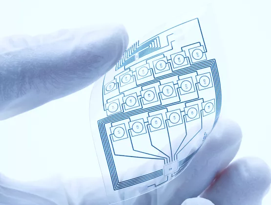
A multidisciplinary team of researchers is developing new methods to collect and analyze sweat for clues about how the body is functioning.Imagine if you could know the status of any molecule in your body without needing to get your blood drawn. Science fiction? Almost – but researchers at the University of Arizona are working on ways to do this by measuring molecules in sweat.When physicians take blood samples from patients, they send the samples to labs to be analyzed for biomarkers. These biological clues indicate everything from cholesterol levels to disease risks, and they can be used to monitor patient health or make diagnostic decisions. The same biomarkers also are found in sweat.Using $519,000 in funding from SEMI-NBMC (Nano-Bio Materials Consortium), Erin Ratcliff, University of Arizona materials science and engineering professor and head of the UArizona Laboratory for Interface Science of Printable Electronic Materials, is leading a project to develop new ways of collecting and analyzing the clues sweat has to offer. Ultimately, this work could allow physicians to use patient sweat samples in the same way they currently use blood samples, for a less invasive and more informative approach to establishing and monitoring patient health.“What’s unique about this is that we are combining biology and engineering expertise to develop a wearable device that will detect molecules in sweat, so you don’t have to get your blood drawn to know the health status of your immune system, your nervous system, indeed, any system in the body,” said co-investigator and sweat biomarker pioneer, Esther Sternberg, MD. “The goal, eventually, is to create a device that will provide physicians and health care providers the ability to monitor your health status continuously and in real-time without needing to draw blood.” Materials science and engineering professor Dr. Erin Ratcliff in her laboratory at the BIO5 Institute at the University of Arizona “We are pleased to sponsor and eager to complete this project with University of Arizona’s impressive team bridging the disciplines of engineering and life sciences,” notes Melissa Grupen-Shemansky, PhD, Chief Technology Officer and Executive Director of SEMI-NBMC. “A concerted interdisciplinary approach at the early stages of R D is relatively new and there is much learning on both sides. The UA team brings unique strengths in both areas and we are excited to be partnering and collaborating with them.”Ratcliff’s co-investigators are J. Ray Runyon, a research assistant professor in the Department of Environmental Science, and Sternberg, research director for the Andrew Weil Center for Integrative Medicine; director of the Institute on Place, Wellbeing, and Performance; and the Andrew Weil Inaugural Chair for Research in Integrative Medicine. Ratcliff and Sternberg are both members of the BIO5 Institute.Standardized Sample CollectionIn order to study sweat, researchers need to collect samples of it, and there are a number of ways to do so.“The obvious idea would be to make a patch that gets information from many pores at once, but the problem is that this creates a space between the patch and your skin, and you have to wait for it to fill up with sweat,” Ratcliff said. “We hypothesize that while you’re waiting, these molecules – the very molecules you’re trying to detect and analyze – are changing chemically.”The team’s first task is to develop new, continuous and hands-free collection devices that deliver high-quality, standardized sweat samples. This will allow health care professionals to gain a more holistic picture of a patient's bodily systems over an extended period, rather than the “snapshot” a blood draw can provide of a particular moment.Currently, sweat labs across the world are using different methods to collect samples, which limits researchers’ ability to compare data. Standardizing the collection method could provide researchers, including medical device developers, with a new degree of confidence in sweat sample data.“High-quality data, with respect to different target molecular biomarkers in sweat, requires that a high-quality sample be collected,” Runyon said. “This will be the first hands-free method that will truly take into account the interplay of the chemistry of sweat, the target biomarker and the device material.” University of Arizona student in classroom testing medtech devices Low-Level DetectionThe team is also developing methods for researchers to detect and analyze neuropeptides in the collected samples. Used by neurons to communicate with each other, these small molecules are involved in biological functions, including metabolism, reproduction and memory. Commercial wearable devices monitor metrics like heart rate, and some use sweat sensors to monitor dehydration level. Measuring neuropeptides, however, will allow researchers to zoom in millions of times closer to investigate stress and relaxation responses at the molecular level.“The idea is that your sweat is reflecting your nervous system – all of the neurotransmitters your body uses to signal between the brain and the rest of the body,” Ratcliff said. “Monitoring this biochemical response continually, over a 24-hour cycle, can inform us about the health of the wearer and also act as a diagnostic tool.”Meet Dr. Ratcliff and the University of Arizona team at FLEX in San Jose, Calif., February 23-26, 2020. Emily Dieckman is Editor at The University of Arizona. Republished with permission from the University of Arizona.
Read More
MEMS technology has changed human interaction with electronic devices. Introduced in the 1990s, the first mass-market MEMS devices were used for inkjet printheads and automotive airbag crash sensors. Today, MEMS are ubiquitous, with billions of the tiny devices adding intelligence and interactivity to smartphones, smart speakers, wearables, automobiles, biomedical devices, remote monitoring and event detection systems, and countless other applications. Integrating MEMS with Flexible Hybrid Electronics (FHE) is an important step in the evolution of this miniaturized intelligent sensing technology, paving the way for its use in new classes of flexible, conformal devices.The integration of the two technologies promises to breed new applications in small form factors but also presents challenges inherent to FHE design and fabrication processes. SEMI’s Nishita Rao caught up with Nathan Pretorius, prototyping and automation engineer, NextFlex, to discuss MEMS-FHE device integration challenges and opportunities ahead of his February 26 presentation, Integrating MEMS Devices in FHE, at FLEX|MEMS Sensors Technical Congress (MSTC) 2020, February 24-27, 2020, at the DoubleTree by Hilton in San Jose, California.Join us at FLEX|MSTC to meet Nathan and other industry influencers advancing innovation in FHE and MEMS sensors. Register now to connect with him at FLEX|MSTC or visit him on LinkedIn.SEMI: Why is integrating MEMS devices into FHE systems important? What new use cases might it enable?Pretorius: The main value proposition of integrating MEMS devices into FHE is that it allows MEMS devices to exist in a different form factor than was possible previously, giving us high-quality MEMS sensors on the flexible and conformable platform of FHE.Ease of application, flexibility, lower cost and rapid iteration on a design are just some of the benefits of FHE devices. And because there are few robust FHE sensors that overlap with MEMS’ capabilities, when you combine the two, you get a lot of compelling uses. That’s why NextFlex is working with agencies and companies to evaluate MEMS’ integration, including using bare MEMS die with microfluidics and promoting new ways of attaching and packaging MEMS die for use with FHE. SEMI: Why is FHE an ideal platform for integrating various types of sensors?Pretorius: MEMS integrated with FHE devices are ideal for rapid design and deployment of data-gathering sensor nodes — which we can iterate for specific applications. A few examples include on-body health monitoring devices for bio-fluids analysis, medical pressure sensors for monitoring blood pressure, and peel-and-stick sensors nodes for infrastructure monitoring. In terms of design and production, FHE devices support rapid prototyping, allowing for instantaneous design-iteration cycles. This speeds design-to-production over traditional rigid PCBs and copper flex because the feedback cycle time between design, manufacturing and testing is shorter, accelerating time to market. What’s exciting about FHE technology is that a variety of sensors or components, including MEMS, can be designed into the base system to easily customize it for a specific application. In addition, our experience shows that when compared to a traditional rigid PCB, an FHE board reduces manufacturing steps and device weight by two-thirds and, perhaps most importantly, converts the device to a thin, conformal shape that makes possible products in new form factors. SEMI: What are the primary challenges to integrating MEMS with FHE? What is NextFlex doing to help device manufacturers address these challenges? Pretorius: There are a few challenges, some of which are device-specific. Most recently, I’ve been focusing on inertial and timing devices, including accelerometers, gyroscopes and resonators. There are a few technical challenges involved in the process of getting the devices from the wafer to an FHE substrate. The wafer processing is very important, especially the dicing and thinning steps. After thinning and dicing, the die is placed onto the FHE substrate. The stresses caused by bonding to the substrate have to be understood and characterized. After placing the die, you then have a calibration step, which is normally performed after the device is packaged. With a MEMS die placed onto directly onto an FHE substrate, calibration then must be done.Finally, the device encapsulation is important, since on an FHE substrate the hard-to-soft material transition is very important to mitigate stresses to rigid component interfaces. We have also been looking at how to work with devices that have damping vents. Flexible encapsulants are inherently more permeable to gases and water vapor than hard encapsulants, so studying the encapsulation of MEMS devices on FHE is another area of interest. NextFlex has been working in a supporting role to evaluate best design practices and best attach and integration methods. In addition to our ongoing collaborative programs, NextFlex is developing the FHE manufacturing ecosystem to include system and component manufacturers and designers, product developers, and materials and equipment providers.SEMI: How do we facilitate closer collaboration between the FHE manufacturing ecosystem and MEMS suppliers such as MEMS device manufacturers, product developers, and materials and equipment providers?Pretorius: It’s important to include manufacturers early in the design process so we can identify challenges up front. That’s why NextFlex spearheads technology road-mapping efforts that include representatives from across the manufacturing ecosystem. We use the roadmaps to prioritize challenges that we can address effectively through collaboration, focusing the industry on solving problems through Project Calls that reveal integration challenges and results from real devices and that tell us how the materials and equipment actually perform with a real device.NextFlex keeps the information flowing, holding quarterly project update webinars to share results. As current devices are optimized for the process in which they will be used, we learn a lot from the project performers who make FHE system demonstrators — and we share that information with the member community. SEMI: Can you point to an example of a successful MEMS-FHE device integration?Pretorius: MEMS-FHE integration is still in the early stages, but we are working on several projects including a DARPA Seedling project for which we have integrated MEMS sensors into FHE systems for testing and evaluation. We plan to continue this work by integrating MEMS and FHE devices using methods that support mass production.SEMI: What would you like FLEX|MSTC attendees to take away from your presentation?Pretorius: We would like to see the FHE community work more closely with MEMS device manufacturers. For example, NextFlex often works with manufacturers to gain access to bare die, which is still a significant hurdle in making devices.The best way to speed things along is to get involved. We encourage FLEX|MSTC attendees to join NextFlex. As a prototyping and automation engineer at NextFlex, Nathan Pretorius explores new print methods for prototyping and automation using novel materials and processes. Pretorius currently focuses on how best to apply software scripting and machine learning to streamline FHE processes. Prior to joining NextFlex, he researched the strengths of roll to roll and screen printing on printed electronics designs, including capacitive touch interfaces, FHE passive component design, and antennas. Nathan holds a Bachelor of Science degree in Graphic Communications from Clemson University. FLEX|MSTC is organized MEMS Sensors Industry Group (MSIG) and FlexTech, SEMI technology communities focused on the growth of MEMS sensors and the flexible electronics supply chain, respectively.Nishita Rao is marketing manager for technology communities at SEMI.
Read More
The GAP9, GreenWaves Technologies latest IoT application processor -- which is being fabbed on GlobalFoundries 22FDX (FD-SOI) technology -- will be sampling in the first half of 2020, according to EETimes (read the whole article here). Mass production is slated for 2021. Greenwaves (which has been an SOI Consortium member for several years now) is a fabless semiconductor startup designing disruptive ultra-low power embedded solutions for AI processing in sensing devices at the very edge. GreenWaves marketing director Martin Croome told EETimes, “We are using the body biasing ability in FD-SOI to allow us to achieve even lower power consumption.” Compared to GreenWaves’ currently shipping product, GAP8 (which is on a 55nm bulk process), GAP9 reduces energy consumption by 5 times while enabling inference on neural networks 10 times larger. This is thanks to architectural enhancements and the move to GF's 22FDX semiconductor process. The new chip delivers a peak cluster memory bandwidth of 41.6 GB/sec and up to 50 GOPS combined compute power at an overall power consumption of 50mW. It enables customers to embed machine learning and signal processing capabilities into battery operated or energy harvesting devices such as IoT sensors in smart building, consumer and industrial markets and consumer and medical wearable devices. GAP9 was showcased at the last RISC-V Summit in San Jose (read the full press release here). [caption id="attachment_29061" align="alignnone" width="400"] GAP9 Block diagram (Courtesy: GreenWaves)[/caption] Some of the (many!) features include: 10 identical high performance, extended ISA, RISC-V ISA cores (cluster of 9 cores for compute-intensive tasks and a fabric controller core for control and communication) Dynamic voltage frequency scaling and automatic body biasing Multiple power states: deep sleep, deep sleep with retentive RAM, low activity, SOC on, SOC on cluster on Click here for a full GAP9 product brief.
Read More
VTT Technical Research Centre of Finland Ltd (VTT) has its sights set high. As a leading global research and development firm , VTT is out to produce bio-interfacing and biodegradable flexible hybrid electronics (FHE) devices that help tackle some of the world’s greatest challenges including environmental degradation and food scarcity.SEMI’s Maria Vetrano interviewed Antti Vasara, president and CEO of VTT Technical Research Centre of Finland, to preview his February 25 keynote, Beyond Flexible Hybrid Electronics: Biodegradable Electronics and Interfacing Bio+Electronics, at FLEX|MEMS Sensors Technical Congress (MSTC) 2020, February 24-27 at the DoubleTree by Hilton in San Jose, California. Join us at FLEX|MSTC to meet Antti and other industry influencers driving innovation in flexible hybrid electronics (FHE) and MEMS sensors. Register now to connect with him at FLEX|MSTC or visit him on LinkedIn.SEMI: What is body-interfacing electronics and what is your vision for bio-interfacing and biodegradable electronics?Vasara: Body-interfacing electronics have existed for decades. Developed in the 1970s, the wireless heart rate monitor is a good example. While continuous heart monitoring with a compact, inexpensive wearable device is widely accessible technology, other bodily parameters, such as cholesterol levels or biomarkers, are diagnosed every time we see a doctor. Establishing a baseline using multiple measurements — before symptoms develop is actually much more effective.That’s where bio-interfacing comes in. Bio-interfacing devices will continuously measure and analyze complex biogenic substances such as sweat, breath, blood and urine. A smart patch for continuous sweat monitoring, for example, would overcome several challenges: supporting electronics functionality in liquid environments, managing the transport of harvested samples to and from the sensor, managing potential contamination, and disposing of samples after measurement.While FHE in principle delivers the right building blocks and is an ideal form factor for a wearable sweat analytics patch, flexible circuits are not ready for out-of-the box interaction with biological matrices. Hence, our mission at VTT is to anticipate and develop the upscaling process know-how required for FHE devices that either interface with biological systems — or that must themselves biodegrade.We’re also focusing on biodegradable electronics because environmentally conscious end-users and manufacturing companies want biodegradable versions of energy-autonomous, label- or sticker-like Internet of Things (IoT) sensors. Typically used for packaging, logistics, environmental monitoring and medical diagnostics applications, these sensors — which have a lifetime of a few days, weeks or months — have become very popular. Unless they are biodegradable, however, they just add to landfill.SEMI: What approaches is VTT using to develop bio-interfacing and biodegradable electronics?Vasara: In our Business Finland-funded ECOtronics project, we are working with our partners to create recyclable and compostable electronics and optics that use renewable resources. For example, devices developed using substrate materials like paper, cardboard or VTT’s in-house-developed nanocellulose films and biopolymer films for environmental monitoring or skin patches can be easily recycled or even biodegrade naturally. Where possible, we use roll-to-roll printing to generate the device circuitry, and on a component level, we have optimized our assembly process towards bare-die component bonding to reduce the overall footprint of non-biodegradable waste per device.SEMI: What use cases do you find most promising and why?Vasara: A prominent example of a single-use test that generates a large amount of waste is the digital pregnancy test. When breaking it down into components, you will find a rigid circuit board with microprocessor, a couple of coin cell batteries, a liquid crystal display, a LED light source and photodiode, and a large chunk of plastic packaging around it. The materials and battery capacity of such a device would be sufficient to run hundreds of pregnancy tests – actually technical overkill.By using printed circuits on biodegradable substrates, bare-die assembled components (ASIC, LED light sources, photo diodes, thin film batteries as power sources) and device packaging composed of biodegradable plastics, we can completely redefine the environmental footprint of single-use tests. We are currently developing a toolbox for our customers to turn their existing conventional test into an ecotronic form factor.Another exciting use case is a sweat sensor that we developed collaboratively with Ali Javey, Ph.D., professor of Electrical Engineering and Computer Sciences, UC Berkeley, and the co-director of Berkeley Sensor and Actuator Center (BSAC). Together with his team, we created a wearable electrochemical sensor for continuous sweat analysis during exercise. With the UC Berkeley group providing the chemistry to monitor N+, K+ ion and hydration levels in sweat over the duration of several hours, VTT delivered the underlying sensor platform, featuring the printed sensor electrodes and sweat harvesting microfluidic channels for fluid management and transport. It’s exciting to see what we can achieve by combining techniques from different disciplines, in this case electrochemistry, printing, packaging and microelectronics.SEMI: How can industry enable the development/manufacture of flexible FHE devices? Where does VTT fit into the ecosystem?Vasara: As many FHE devices target large-volume markets, scalability of manufacturing is key: How can I get from one device (= working prototype) to a handful of devices (= feasibility study), to thousands (= pilot manufacturing), to a million (= mass manufacturing) without compromising the quality of the system’s performance and reliability?Access to upscaling infrastructure is essential for the development of novel FHE devices and methods, but infrastructure is expensive. That’s where our establishment of a roll-to-roll pilot printing line to bridge the gap between laboratory R D and mass manufacturing has proved invaluable. We can provide a unique worldwide upscaling infrastructure for advanced FHE devices, with a strong focus on large-area roll-to-roll processes and hybrid assembly. This service removes our customers’ burden of high infrastructure investment in early development stages and it allows us to guide customers along their development path, from prototype to mass production.Watch our video: VTT pilot manufacturing for diagnostics and wearablesSEMI: Is there anything else that device manufacturers need to know in order to succeed?Vasara: In my eyes, the success of FHE devices eventually depends on several factors: It requires a high degree of automation, well-optimized processes, reliable supply chains, and perhaps most importantly, clear standards and rules for designers to guarantee flawless interoperability of all the different elements on a flexible and hybrid circuit. Let us not forget – we are trying to marry electronics with printing, biology, packaging, microfluidics, injection molding and other fields of expertise.We recently finalized the compilation of a set of design rules for publication in our state-of-the-art overview of printed and hybrid electronics manufacturing methods. You can download the overview, PrintoCent Handbook, for free.SEMI: What would you like FLEX|MSTC attendees to take away from your presentation?Vasara: The latest technologies and innovations in microelectronics, MEMS, printing, materials, and biosensors provide us a toolbox for true innovation in the FHE space. Now we need cross-disciplinary thinking and daring steps to combine different manufacturing methods and skill-sets. The ideal cross-disciplinary team might include: The printing engineer who knows how to design contact pads for a bare-die IC assembly The biologist who knows about the thermal and mechanical stress in a printing environment to design processes for bio-functionalization of surfaces The electronics engineer who knows how to optimize a circuit powered with an enzymatic biofuel cell The number of sensors deployed on (or inside) our body, in our drinking water, in our cars, on our fields, in our pets, and everyday products will surely grow. Let us make sure they leave the smallest environmental footprint possible.Antti Vasara, Ph.D. has been the president and CEO of VTT Ltd since 2015. VTT is a visionary research, development and innovation partner with over 2000 people and a turnover exceeding 250M EURO. Vasara is president of EARTO (European Association of Research and Technology Organisations) and is chairman of the board of Palta (Finnish Service Sector Employers). In addition, he is a non-executive director of Elisa Oyj (largest communications operator in Finland) and a board member at EK (Finnish Confederation of Industries).He has served on several high-profile groups on industrial and innovation policy of the European Commission, in addition to several groups in Finland on artificial intelligence and research policy. Previously, Vasara spent close to 25 years in private industry, working at Nokia, Tieto, SmartTrust and McKinsey Company. Earlier in his career, he was a researcher in optical communications with 20+ peer-reviewed articles and one international patent. Vasara holds a Doctor of Science (Technology) degree from Aalto University in Finland.For more information about VTT’s work in bio-interfacing and biodegradable FHE devices, visit VTT Research. FLEX|MSTC is organized MEMS Sensors Industry Group (MSIG) and FlexTech, SEMI technology communities focused on the growth of MEMS sensors and the flexible electronics supply chain, respectively.Maria Vetrano is a public relations consultant at SEMI.
Read More
It should really be called SOI photonics – not just silicon photonics, quipped Soitec CTO Christophe Maleville at the SOI Consortium Japan event last fall. You’ve got to have SOI for the waveguides. There are megatrends driving significant growth in photonics – and they were all covered at the event. This is the final post in our coverage of the SOI Consortium’s Japan event (thank you for your patience!). It covers the photonics-related presentations by Soitec, Leti, Cisco/Luxtera, GlobalFoundries, Cadence and TowerJazz. Most of these presentations are now posted on the SOI Consortium website – you can access them if your organization is a member of the consortium. By way of reminder, the Japan SOI Symposium was a great success, with both days well attended. In case you missed our previous posts about the event, you’ll want to go back and read them, too. The first post covered the 5G/RF-SOI presentations by ST, Toshiba, Incize, GF, Silvaco and Sitri – you can read it here. The second post on the event covered eight very informative presentations on SOI in IoT and automotive by NXP, Dolphin Design, Leti, Silvaco, Arm, I-fuse and Secure-IC – you can read that here. Note that you can click on any of the illustrations to see enlarged versions. And now without further ado, here are the summaries of the photonics presentations. SOI Enabling Photonics – Ecosystem and Market Outlook – by Aziz Alami-Idrissi, GM Specialty SOI, Soitec. [caption id="attachment_28773" align="alignleft" width="233"] (Courtesy: Soitec SOI Consortium)[/caption] The megatrends in SOI photonics are: 5G (for more bandwidth, HPC, edge quantum computing), data centers (for high data rate transceivers and high-switch bandwidth), sensors (lidar, gas/chemical and gyroscopes) and biosensors (especially for medical). These are driving big changes: the 44% CAGR means the market is growing from a current TAM of about 500M$ to over 4B$ in 2025. One thing that’s really interesting is the expansion of the photonics market into these new fields in the next few years. While in 2019 90% of the photonics market served data center applications (the other 10% is for long haul), in 2025 optical I/O’s will account for over a third of the photonics market TAM. The other applications making an impact include AI, quantum, lidar (which will move into high-volume manufacturing in 2024) and medical sensors (hitting high-volume in 2023). For its part, Soitec is strengthening its portfolio with 8” and 12” large product coverage, new product sampling engaged, and extended features including newer engineered layers and RF immunity. Advanced Silicon Photonic Solutions Leverage SOI Technology – Eleonore Hardy, Business Development Manager, Silicon Photonics, CEA-Leti [caption id="attachment_28769" align="alignright" width="358"] (Courtesy: Leti SOI Consortium)[/caption] Leti helps companies make photonics products they can bring to volume foundries, explained Hardy. (btw, they’re presenting 21 (!) papers – including 5 invited – at PhotonicsWest 2020. Read about that here). You want to do integrated photonics to bring down costs, reduce power consumption, and scale (for higher volumes and reduced footprint). There are essentially three substrate choices: InP, SiN or SOI. SOI uses CMOS processes, so it’s low-cost and can be used in high-density photonic integrated circuits. What about the laser? Leti has developed III-V on silicon bonding, so you can have the laser on 4” III-V with a 300mm CMOS process (this is what Intel’s doing). They’re moving to 300mm wafers, 3D and advanced packaging. While communications is the big application realm, Leti is also applying photonics in automotive, medical, environment and computing. In the computing realm she gave the example of the European QuantERA SQUARE (Silicon Photonics for Quantum Fibre Networks) project for which Leti is doing the quantum emitter for absolute security and computing, wherein the transceiver/receiver for quantum cryptography integrates a hybrid III-V on silicon pump laser. Other examples of their work include miniature, low-cost and agile lidar for automotive and industrial applications (they’re working on a beam-steering emitter for an optical phased array). GlobalFoundries Silicon Photonics Solutions for Wired Infrastructure – Anthony Yu, VP, GF [caption id="attachment_28770" align="alignleft" width="684"] (Courtesy: GlobalFoundries SOI Consortium)[/caption] GF is giving their photonics business a big push. Optical interconnects are the future, said Yu, so they’re putting a lot of money into it. With data streaming multiplying by 3x/year and a current foundry TAM of $63 billion, the opportunity is huge. Fab 10 in Fishkill runs their 90WG process on 300mm wafers. A new process, 45CLO (also on 300mm) for O and C bands is going into the Malta fab. A big focus here are optical transceivers that convert RF signals to light. They see RF on SOI in a monolithic solution is needed to serve 100Gbs applications. They’re also moving to co-packaging optics: the packing technology will surround it with photonic chiplets. Customers have indicated that pulling the signals off the chips is limited by power, so they’ve worked hard on the fiber attach with MEMS and packaging technology for co-packaging. GF relies on substrate providers for high-quality SOI, and they have a world-class development team, he concluded. Integrated Electro-Photonics Design Platform – A multi-physics, multi-fabrics system design solution – Scott Li, Sr. AE Manager of Custom IC Platform, Cadence [caption id="attachment_28771" align="alignright" width="374"] (Courtesy: Cadence SOI Consortium)[/caption] This talk focused on photonics design challenges and solutions – including the CurvyCore™-based PDK for waveguide creation modal properties calculation that Cadence will soon be announcing. It’s a math-based engine that generates complex curvy shapes to support photonics. The first design challenges, said Li, are at the circuit level: how to do the schematics. The detailing tools, timesteps management and circuit simulation need to give the user the best performance. Cadence is working in close collaboration with a company called Lumericable on this. The next set of design challenges come at layout – especially generating curvilinear layout for any shape so that there are no gaps in connections. This is where CurvyCore comes in, fully automating layout and making it easy to modify. This includes place route, DRC and LVS for curvy shapes. The final challenge is at the system level. There is work to do here, but Cadence is collaborating closely on solutions with key partners. The ultimate goal is for photonics layout and editing to be available with all the features designers get in electronics editing. Silicon Photonics for High Volume and High Performance Optical Interconnects Applications – Thierry Pinguet, Technical Leader Engineering, Cisco /Luxtera [caption id="attachment_28772" align="alignleft" width="396"] (Courtesy: Cisco/Luxtera SOI Consortium)[/caption] Over the last decade there’s been steady growth in optical high speed interconnect solutions, mainly driven by HPC, enterprise, and especially the hyperscale datacenter. The largest volumes are for intra datacenter interconnect (between servers). Now mobile applications for backhaul are also driving volume for high speed optical interconnect for 5G network implementation. ASICs and photonics are getting closer as the industry moves to put them in the same package. But everybody does silicon photonics differently (even within Cisco). Luxtera tries to use the same infrastructure as electronics, but patterning is still a challenge: it’s not 90o “Manhattan” style. The wafers are no problem – they work with leading wafer suppliers like Soitec and SEH. They have explored a “double SOI” substrate (like a mirror), which showed large insertion loss improvements in grating couplers . For the electronics and the laser (MEMS), they do a micropackage, although at one point they also did monolithic integration. For better performance, they’re moving to TSVs. A hot topic is ASIC and photonics co-packaging. You can use optical tiles, but then the light is remote, like a power supply. No matter how you do it, though, the bottom line is that silicon photonics is the only way forward for the data center. PH18: World’s First Open Commercial Silicon Photonics Process and PDK from TowerJazz – Masanobu Kumazaki, Engineer, TowerJazz. This presentation was given in Japanese without translation into English, and is not available on the consortium website. But the slides showed at the event indicated that their PH18 is the world’s first open commercial silicon photonics offering. For optical transceiver components, silicon photonics provides another opportunity for a specialty foundry. It is a high-growth market. The TowerJazz offering is 220nm SOI, and uses standard EDA tools from Synopsys, Cadence and Mentor for design flow.
Read More
The march of innovation in semiconductor microfabrication technology over the past 60 years has produced electronic devices and information systems that have transformed industries and lives around the world. And while advances in chip technology continue to make it possible to collect, transmit, store and process more data for a rapidly growing universe of applications, the pace of innovation is now facing strong headwinds. Powered by chip innovation, data centers have become massive centers of information processing but, on the downside, enormous consumers of electricity. Today, the power-hungry hubs account for five percent of the world's electricity usage, a proportion that is growing every year, raising important questions about sustainability. Compounding the challenge, the pace of Moore's Law, for decades the engine of electronic device and information system innovation, has slowed. While the research and development of state-of-the-art semiconductor fine processing technology remains robust, developing the advanced manufacturing technology for mass-producing more sophisticated electronics devices is becoming harder, as is ensuring business profitability."It has become difficult for semiconductor technology to continue to evolve as it has in the past," said Akira Minamikawa, Research Director of Technology Research at IHS Markit, who moderated the Semiconductor Executive Forum – View by Top Two in the Era of Digitalization on opening day of SEMICON Japan 2019 at Tokyo Big Sight. Held at the SuperTHEATER, the forum featured Terushi Shimizu, representative director and president at Sony Semiconductor Solutions, and Atsuyoshi Koike, president at Western Digital Japan, two industry powerhouses that could figure heavily in the future of digital technology. SuperTHEATER, the main stage at SEMICON Japan 2019 Image sensors evolve to become eyes of AIImage sensors are becoming eyes of artificial intelligence (AI) and intelligent systems that monitor people and events worldwide, collecting data that one day could help puzzle out growing social challenges such as energy conservation and traffic congestion. With 51 percent market share on the strength of its industry-leading technology, Sony Semiconductor Solutions dominates the image sensor market. Despite last year’s global semiconductor industry slump, the company’s “business continues to enjoy strong growth and we are very busy,” said Shimizu, who attributed the company’s robust performance to the rising importance of the social role of image sensors and the expanding number of applications they support.The success of the company’s image sensors can also be traced to its division of the image sensor market into two application categories: "Imaging" focuses on capturing beautiful image data, while "sensing" aims to collect data that accurately describes the state of a subject and its surroundings."In 2019, sales of imaging products for smartphones grew rapidly,” Shimizu said in his market overview. “This is due to the average annual 15 percent growth rate of multi-camera smartphones, with some phones today featuring seven cameras, and an average annual growth rate of 20 percent in sensor size to produce higher image quality."But Shimizu cautioned that Sony Semiconductor Solutions doesn’t expect the smartphone sensor market to maintain that fast growth rate."The imaging market is expected to grow until 2022, but after that, the sensing market will drive market growth,” he said, adding that the company’s “capital investment plan is based on this scenario."AI will be key in catalyzing growth of the sensor market as integrations of AI processing engines and sensing images grow in sophistication to capture images undetectable by the human eye, Shimizu said. AI will extract insight from captured image data. For its part, Sony will apply its layer stacking technology to sensing products."By stacking an AI processing engine, we want a significant portion of the recognition processing done within the sensor chip," Shimizu said.One sensor the company already offers collects in-depth information for indirect time-of-flight (ITOF) 3D ranging for new user interfaces relying on autonomous or gesture control for robotics. The sensor “was first used in smartphones in 2018 and saw widespread adoption in 2019," Shimizu said.Sony Semiconductor Solutions plans to focus on developing new sensors for integration with their ultrasonic cousins. Aided by optical deflection technology, the sensors will be used for product quality inspections during manufacturing.With the company’s growing strengths in sensor technology, it hopes “to increase sales of sensors from a few percent of the company’s total sales in 2018 to 30 percent in 2025,” Shimizu said, pointing to its goal "to capture 60 percent share of the image sensor market by 2025."Data as one way to spread happinessAt the heart of consumer devices such as smartphones and computers and also cloud servers, NAND flash has made it possible to process vast troves of data anytime, anywhere. In recent years, the technology has enjoyed stronger adoption for use as the storage medium of choice for edge computing, stationed between end devices and the cloud to help streamline data utilization. But the technology isn’t merely about making smarter use of bits and bytes."We would like to promote the technology development that can support the use of data to bring happiness to people around the world," Koike of Western Digital Japan said. The company calls data that contributes to individual happiness and helps solve social issues "data for good" and, like the Sony Semiconductor Solutions bifurcated classification of the image sensor market, categorizes information into “big data” and “fast data.”For example, big data can leverage AI to drive dramatic improvements in the interpretation of test data and, ultimately, the diagnostic accuracy of mammography for breast cancer screening, aiding in early detection to help save lives, Koike said. Fast data can be harnessed to analyze data collected from a manufacturing equipment line in real time to improve production efficiency. The company’s plant in Yokkaichi, Mie Prefecture, which the company operates in cooperation with Japanese memory manufacturer Kioxia, already uses fast data to bolster production.More NAND flash innovation and greater supply capacity are critical to developing "data for good," Koike said. "It is difficult to expand clean rooms at the same pace as data usage grows. In order to continue to advance technology and enhance supply capacity, we need to adopt new ideas for building production lines. We need a smaller equipment footprint, shorter cycle time and higher throughput."Semiconductor market shows signs of recoveryIn their discussion of the short-term outlook for the semiconductor market, Shimizu and Koike pointed to the importance of strengthening the talent pool of Japan’s semiconductor industry as global competition heats up with China’s pursuit of semiconductor independence and the industry pulls out of the 2019 slowdown fueled by weak memory prices. While Sony’s business has been buoyed by strong image sensor demand for smartphones, the devices “did very well, but other applications didn't," Shimizu said. Even the image sensor market stagnated.Despite the 2019 slump, market conditions and capital investments by semiconductor manufacturers have been on the upswing."In the second half of 2019, the Chinese market showed signs of recovery triggered by 5G,” Shimizu said. “In 2020, this movement is going to be in full swing around the world and we will be busier than last year."Koike agreed: "The semiconductor market for data centers will recover with 5G. The hard disk shortage is already an indication of a recovery, a turnaround that will undoubtedly extend to solid state drives (SSDs). In addition, advances in autonomous driving technology will ensure continued growth of the automotive semiconductor industry.”Japan should embrace international competition, not fear China's pursuit of chip independenceIt's no secret that China is investing heavily in its semiconductor development capabilities to move up the microprocessor value chain. Minamikawa posed the question: How should Japanese chip companies navigate the shifting regional balance of power? "It is natural for China to strive to establish domestic procurement of semiconductors that are fundamental technologies for various industries,” Koike said, “I think the efforts of Chinese companies are outstanding in that they are not pursuing short-term results, such as improving yields in the near future, but are making efforts with an eye to achieving results in 10 years. Japan has a variety of options including working with China to create joint ventures and competing head-on. Regardless of which choice we make, however, it is imperative for the survival of domestic companies that Japan maintains its technological competitiveness to remain ahead of China."Shimizu said that Sony’s “Chinese customers are quick to take action and study extremely hard. We often have opportunities to share our roadmap with them and explore innovation opportunities together. Before, they were passive and relied on us for insights into new technologies, but now they are more assertive and I sense that they will start to drive innovation.”Koike added that "although Japanese companies often talk about business globalization, neither Chinese nor American companies say much about it. While global expansion is a major requirement for business, I think Japanese companies need to focus more on the Japanese market overall, not just when they think about the growing competitiveness of Chinese companies." L-R: Akira Minamikawa, Research Director of Technology Research at IHS Markit; Atsuyoshi Koike, president at Western Digital Japan; Terushi Shimizu, representative director and president at Sony Semiconductor Solutions Talent key to bolstering competitiveness of Japan’s semiconductor industryMinamikawa of IHS Markit didn’t mince words in describing the talent shortage in the Japanese semiconductor industry as “grave,” saying that “the workforce challenge is not endemic to the electronics industry as evidence grows that the number of people obtaining doctorates in Japan is falling and the educational level of the Japanese population as a whole is in decline.”Three years ago, Shimizu interviewed professors on Kyushu island for insights into Japan’s talent shortfall. He came away feeling that “Japanese semiconductor companies were not sufficiently communicating the industry's talent and innovation needs to professors. To help professors and students better grasp the appeal and potential of the industry, we have started to send frontline engineers to universities to educate students and instructors about their work and careers. Expecting corporate HR departments to alone solve the talent shortage won’t work.”"In Japan, if you advance to a doctoral course, you will have a hard time getting a job, which is a strange situation,” Koike said. “Companies and universities need to work together more closely to better understand how to attract and hire doctoral graduates."Minamikawa said companies must have strong leaders with clear missions to attract the right talent, but Koike pointed to the drawbacks: "The image of a company with a strong leader seems to be cool, but it also has a downside because engineers stop thinking for themselves and wait for instructions from the top. I believe it is important for company leaders to have ongoing discussions at all organizational levels and lead the way in times of confusion."Shimizu agreed, citing his own company as an example."Thankfully, our company is very busy right now,” he said. “However, some employees are starting to request more time to think about how to improve the quality of their work. To maintain and strengthen our competitiveness and continue business growth, I believe it is important to cultivate an environment that encourages each employee to take more time to think for themselves."Motoaki Ito is the CEO of Enlight, Inc. and a reporter for SEMI. Mayumi Amagai is a marketing manager at SEMI Japan.
Read More
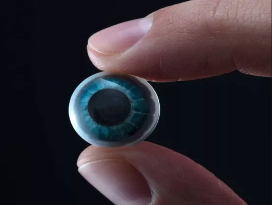
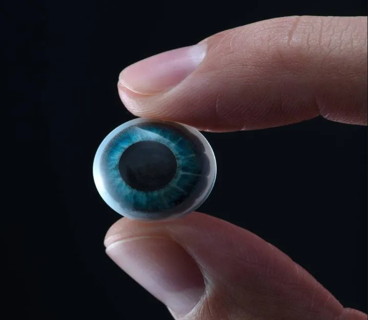
Today’s mobile devices are smaller, more power-efficient, and have more capability than we could have imagined just a decade ago. Offering ever-increasing levels of user functionality, mobile devices are now ubiquitous, and are rapidly becoming the primary mechanisms through which we interact with the digital world, our physical environment, and one another. An unintended side effect of our dependence on the current crop of mobile devices is that they are driving us to distraction.A major industry dynamic will shake things up for the better. Sensors are getting smaller and more efficient, and they’re offering attractive new functionality, giving us the ability to monitor our air and water quality, assess potential toxins in our food sources, and analyze personal health conditions, to name a few use cases. At the same time, the realization of flexible hybrid electronics (FHE) through new materials and production processes, better integration with other electronic components, more efficient energy production and consumption, and pervasive wireless connectivity are fueling the next generation of devices and experiences. What can we expect from tomorrow’s mobile devices — and how can we manage them, instead of having them manage us?SEMI’s Nishita Rao caught up with Mike Wiemer, Ph.D., VP of Engineering, CTO and co-founder, Mojo Vision, to preview his February 25 keynote, The Art of the Possible, at FLEX|MEMS Sensors Technical Congress (MSTC) 2020, February 24-27 at the DoubleTree by Hilton in San Jose, California.Join us at FLEX|MSTC to meet Mike and other industry influencers advancing innovation in FHE and MEMS sensors. Register now to connect with him at FLEX|MSTC or visit him on LinkedIn.SEMI: Mojo Vision has conducted its own research on human interaction with mobile devices. Why is this important?Wiemer: Our mobile devices have given us access to the information we need and want, improving many aspects of our lives. But our devices have also influenced our relationships and attention to our environment in negative ways. We believe that the next mobile computing platform must improve this situation. Instead of pulling us away from the moment, our devices need to embrace more human-centric engagement while still letting us access information that improves our quality of life. Mojo Vision has worked to understand this problem through our own studies and research so we can better develop an approach to address it. SEMI: How are key technical trends driving size, efficiency and capability advancements in mobile devices?Wiemer: Tiny low-power sensors are enabling ever-smaller feature-rich mobile devices that run longer on a battery charge. Smartwatches are a good example. Just a few years ago, smartwatches were not that much more than small screens on our wrists. Today, we have GPS, EKG/health monitoring, and cellular wireless interfaces all inside the same form factor.As this trend continues, we at Mojo Vision predict that our devices will continue to shrink and become even more personal: They’ll be more continuously worn and matched to our own needs and behaviors. This trend towards invisible personal devices is something we’re trying to accomplish with our solutions at Mojo Vision.SEMI: What is Mojo Vision’s concept of “Invisible Computing?” Wiemer: Our vision of Invisible Computing is based on the idea that our wearable devices should be invisible to those around us, encouraging more human interactions. These wearables should be invisible and unobtrusive to users themselves. Our Mojo Lens, which contains a full display and sensors housed inside a contact lens platform, exemplifies this vision. Using proprietary microelectronics and the world’s densest microdisplay to layer digital images and information seamlessly, Mojo Lens is redefining augmented reality. Our mobile devices today continue to increase the quantity and magnitude of interruptions. We think that shouldn’t happen. As a socially invisible device that delivers contextual, relevant content, the Mojo Lens lets us go about our daily lives, naturally interacting with other people while simultaneously enjoying the benefits of augmented reality. We think Invisible Computing can change our relationship with our devices, as well as seemingly give us superpowers. For more information, download the Mojo Vision report, Device Distraction: Understanding the Problem, Re-Thinking the Solution.SEMI: Can you tell us more about Mojo Lens?Wiemer: At its foundation, Mojo Lens is a nanoLED display, radio and sensor platform, integrated using flex technologies, and placed on your eye to provide important information. Mojo Lens can elevate or suppress this information to decrease reliance on your other devices.Unlike your smartwatch or smartphone, which react to you in a binary manner because they don’t have enough information to make autonomous decisions, Mojo Lens understands the context of your experience. That’s because it’s based on our Invisible Computing platform, which can understand your activity. Mojo Lens recognizes if you’re engaged in a conversation, driving or having a coffee, and it reacts with information accordingly.Mojo Lens could act like a real-time interpreter, for example. When someone speaks to me in a language I don’t understand, I should see “subtitles.” Or if I’m having a conversation with someone, Mojo Lens wouldn’t interrupt me with a notification at that moment. For the 92% of Americans who are interrupted by their devices during conversations every day, this prioritization can boost productivity. More importantly, it can improve the quality of our connections with the people around us.Mojo Vision’s microLED platform offers a world-record pixel pitch of over 14,000ppi and pixel density of over 200Mppi², making it the smallest, densest display for dynamic — or moving — content. SEMI: What would you like FLEX|MSTC attendees to take away from your presentation?Wiemer: It feels like the speed at which people are defining important problems and tackling them is increasing every year. And there are so many important problems to solve: space travel, autonomous driving, electric vehicles, alternative energy, quantum computing, lifespan extension, increased food production, brain-computer interfaces, AR/VR. All these problems seem impossible and “crazy,” until some group of people comes along to put a framework in place that can address them. Interestingly, these frameworks aren’t necessarily new. Rather, they build upon existing technologies and capabilities.MEMS sensors and FHE are good examples. From smart textiles, flexible displays and biological sensors to miniature radars, MEMS sensors and FHE technologies are essential building blocks. Many of the big problems we can imagine today will be solved by stacking today’s MEMs and FHE technologies in imaginative new ways. So what do we do next? I’d like to encourage FLEX|MSTC attendees to first define the problem to solve and then define the technology — rather than starting with the technology solution. Mike Weimer is a serial entrepreneur and proven science and technology leader in complex systems development and integration. Before co-founding Mojo Vision as CTO, Weimer co-founded and served as president at Solar Junction, a high-efficiency solar cell company (acquired) where he and his team set two world records for the highest-efficiency solar cells ever made by humans.After Solar Junction, Wiemer joined New Enterprise Associates (NEA) as an Entrepreneur in Residence where he sourced new investments and helped portfolio companies to develop their business and funding strategies. He is a board director at Stratio Corporation and an advisor at Stanford’s StartX Accelerator. He holds a B.S., M.S., and Ph.D. in Electrical Engineering from Stanford University.For more information, visit Mojo Vision.Interested in engaging with the MEMS sensors supply chain? MEMS Sensors Industry Group is a SEMI technology community that enables professionals in the MEMS and sensors industry to accelerate business results by addressing common challenges and opportunities.Nishita Rao is marketing manager for technology communities at SEMI.
Read More
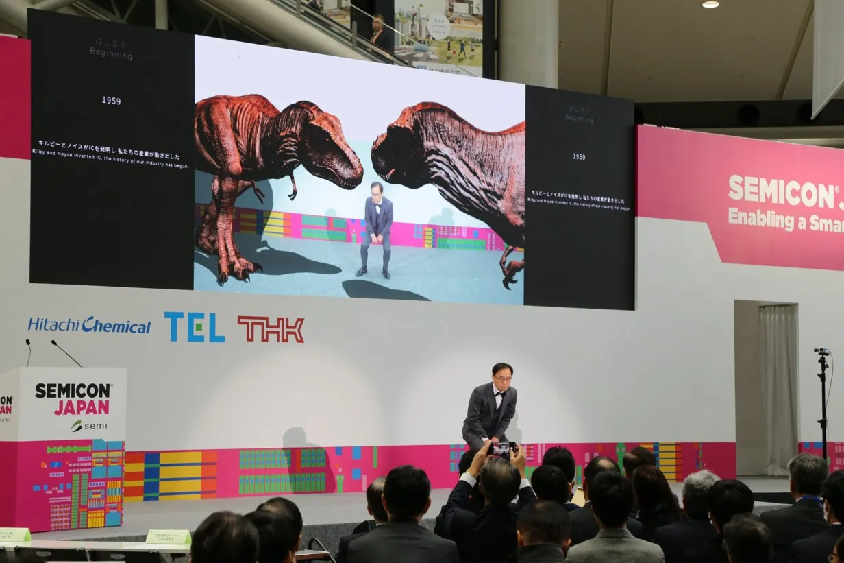
Augmented reality (AR) tyrannosauruses towered on-screen as I interacted with the creatures in a mix of prehistoric and cutting edge. Or, rather, my AR double was doing the playacting. Minutes later, virtual doppelgangers of a small lineup of chip industry executives cut the ceremonial ribbon. Seemingly sweeping away the winter chill, the opening of SEMICON Japan 2019 dazzled with smart technology and the promise of lives, cities and workplaces transformed, with uber-intelligent applications in full display at Tokyo Big Sight. But what resources does the industry need to harness to drive the next era of innovation? The semiconductor industry’s unwavering passion and young talent are key, said Hiroshi Imano, Chairperson of the SEMICON Japan Initiatives Committee, in his opening keynote. And hardly any region of the world is in a better position to help realize that future than Japan, Imano said. The region supplies one third of the equipment and more than half of all materials to the global semiconductor manufacturing industry.Talent was also top of mind for SEMICON Japan 2019 keynote speaker Makiko Eda, Japan's Chief Representative Officer at the World Economic Forum (WEF). Serving as a platform for public-private partnerships, the organization's mandate is to tackle global issues such as climate change and geopolitical strife in making world more resilient to risk and, by extension, more sustainable.Spanning ecology, economy, technology, society, geopolitics and industry, that mission includes reskilling and upskilling a billion people over the next decade, a high priority for WEF, which hosts a conference every January in Davos, Switzerland. The theme of this month's conference – Stakeholders for a Cohesive and Sustainable World – reflects the vital importance of building the international partnerships and global consensus necessary to achieving WEF's goals.One key to that sustainability will be technology and Arm, a global chip design company, will play a key role, with the company’s chips touching over 70 percent of the world’s population, Arm president Yuzuru Utsumi said in his keynote. Today, Arm is driving toward an ambitious goal: Ship 100 billion chips from 2017 to 2021 – the same number produced over the previous quarter century – by powering advances in mobile computing, server and networking infrastructures, and automotive applications.Arm’s innovation ecosystem of more than 1,000 partners will deliver these chips as they continue to work together to develop differentiated technology. Arm plans to increase investments not only in its primary processor business to accelerate market share gains but in the company’s new IoT business to create new revenue streams. The goal: Deliver long-term sustainable growth, Utsumi said. SEMICON Japan 2019 showcases SMART manufacturing and transportation Billed as a showcase of smart technologies, SEMICON Japan 2019 delivered with an array of eye-grabbing exhibitions in the popular SMART Applications Zone. In the SMART Transportation area, the automatic operation pavilion featured a car equipped with open-source software for autonomous driving. The exhibitor, Tier IV, aims to help lead the early commercialization of self-driving vehicles through the adoption of its software, Autoware, which makes it easier to develop self-driving vehicle prototypes using low-power platforms.Sony Semiconductor Solutions demonstrated a vision sensing processor designed to guide autonomous drones. Using two cameras, the processor measured the changing distance between visitors moving about the exhibit and stationary objects in real time, indicating proximity in hues of red (nearby) and blue (at a distance). Many visitors were wowed, describing the multichromatic display as futuristic.Others rode a simple wooden swing hanging by two ropes, but from dizzying heights thanks to Solidray’s Duo-Sight, a virtual reality (VR) system that projects 3D images stretching from wall to floor for immersive experiences. One visitor thrilled at how riding the swing, suspended only a few feet from the floor, felt like soaring on a flying trapeze. Target applications for the technology include virtual rides at amusement parks and presenting interior design options to homeowners.In the SMART Manufacturing area, one highlight was the demonstration by the National Institute of Advanced Industrial Science and Technology (AIST) of a remote-controlled Minimal Fab System designed for low-volume, high-mix chip production with little staffing. Designed to increase production efficiency, the system allows a circuit designer to manufacture a semiconductor by singlehandedly operating equipment up and down the production line. Controlling nearly 50 pieces of equipment, the Minimal Fab System on display manufactured chips that were verified for functional operation and exhibited afterwards.On the SMART Applications stage, exhibitors DENSO and Toyota Motor Corporation announced a new joint venture to conduct research and advanced development of the next-generation in-vehicle semiconductors critical to electric and autonomous vehicle innovation. The venture, operating as MIRISE Technologies, will combine Toyota’s mobility expertise with DENSO’s in-vehicle component prowess. The goal is to build a rapid, competitive development system by 2030, said Yoshifumi Kato, executive director of the DENSO Research and Development Center, and president and representative director of the venture. On track to begin work this year, MIRISE will span three fields of technology development: power electronics, sensing and SoC (System-on-a-Chip). The name MIRISE combines word the Japanese word "mirai" (future) with "rise."Business Continuity PlanningNatural disasters and other emergencies are an ongoing threat to uninterrupted business operations across the semiconductor manufacturing supply chain and particularly in earthquake-prone Japan. To better prepare for business disruptions and restore normal operations as soon as possible after disaster strikes, more companies are teaming on Business Continuity Planning (BCP).THK's Seismic Isolation Experience Car demonstrated one technology designed to help – a seismic isolation device. The car shakes like an earthquake to give people inside a taste of how a building heaves and sways during a quake with and without the device deployed. Visitors were struck by how much the isolator dampens tremors to prevent or minimize damage. In the BCP seminar, representatives from Sony Semiconductor Manufacturing, THK, DISCO and Team Engineering Consulting shared lessons learned from actual disasters and discussed the critical importance of daily disaster drills. Yukihide Keigo, Executive Engineer in charge of Products and Development at Sony Semiconductor Manufacturing, recounted how the company’s Kumamoto Prefecture plant struggled for 96 days to restore full operations after the facility sustained heavy damage in the 2016 earthquake. Keigo said the plant lacked the structural reinforcements necessary to withstand the impact and fell prey to poor planning and accountability. The Kumamoto plant has since implemented measures – structural and procedural improvements – that more accurately account for seismic risks to ensure full recovery within 56 days. The plant’s new procedures include emergency drills for staff including night-shift workers.Innovation abounds at six SuperTHEATER forumsSEMICON Japan 2019 was held in the West and South Halls of Tokyo Big Sight as organizers of the Tokyo Olympics occupied the East Hall, the exhibition's usual home at the venue, to prepare for the 2020 games. For the first time, the main stage, SuperTHEATER, was set up in the cavernous arena near the main entrance. The SuperTHEATER featured six forums over three days. Semiconductor Executive Forum – View by Top Two in the Era of Digitalization with thought leaders from IHS Markit and Sony Semiconductor Solutions SMART Connectivity Forum – Infinite World Brought by 5G Innovation with experts from Softbank and Nokia Solutions Networks SMART Transportation Forum I – Front-line of Automated Driving featuring speakers from Intel and DENSO SMART Transportation Forum II – Revolution of Sky Transportation, supported by the U.S. Commercial Service in Japan, with presenters from Ministry of Economy, Trade and Industry (METI), Subaru and Bell Helicopter Manufacturing Innovation Summit – Issues and Innovation: What will Drive Growth to 2030 featuring thought leaders from VLSI Research, Applied Materials, KLA, Nikon and Tokyo Electron Mirai Vision Forum – Future Relation of Technology and Body 2.0 with speakers from Leave a Nest, Ory Lab and Autonomous Control Systems Laboratory The Mirai Vision Forum highlighted advanced technologies that could lead to societal improvements. One presenter, Kentaro Yoshifuji, CEO at Ory Lab, recalled how, as a child, he once stayed home from school while recovering from an illness. His imagination in full flight, the youngster imagined having a clone that could attend school and be with his classmates. The experience eventually inspired him to develop OriHime, a robot that gives socially isolated people a way to communicate with friends or colleagues remotely. Originally developed for physically impaired people, OriHime today is used to help the able-bodied. The robot is situated with the companion and the user operates OriHime remotely. A camera and monitor in OriHime’s face provide the visual and audio connection and the user controls the device with a smartphone or tablet or, for those who are paralyzed, through eye movement. One potential application: With OriHime stationed at a business office, working mothers could use OriHime to telecommute to better balance their careers with their parenting responsibilities at home. The robot would be a mother’s go-between, enabling her to communicate directly with colleagues.The next generation of innovators also took the stage as five teams presented innovative business ideas in friendly competition. The top prize in The TECH CAMP Hackathon went to the group that hatched an ingenious plan to develop a jacket that trains users to move their bodies in preprogrammed ways. For example, legendary Japanese professional baseball player Shigeo Nagashima could wear the gear while batting to program the device, then give the jacket to someone who’s never swung a baseball bat. The jacket would help the user replicate Nagashima’s swing. Now comes the real work of any innovator – executing on the vision.And then came two soccer-playing artificial intelligence (AI) robots that squared off and ... Scored! The demonstration by the Toyota National College of Technology started as a research project by Toyota National College students in 2002. The young innovators designed and developed all the robotic hardware and software from scratch. Looking ahead to SEMICON Japan 2020!SEMICON Japan 2019 not only gathered leading Japanese semiconductor materials and manufacturing equipment providers to demonstrate their latest innovations. The premiere regional event also provided insights on key trends critical to the entire electronics manufacturing supply chain. This year’s event drew more than 51,000 visitors and 695 exhibitors from 15 regions filling more than 1,700 booths.SEMICON Japan 2020 returns to East Hall at Tokyo Big Sight in December 2020. I look forward to seeing you there!Jim Hamajima is president of SEMI Japan.
Read More