downloadGroupGroupnoun_press release_995423_000000 copyGroupnoun_Feed_96767_000000Group 19noun_pictures_1817522_000000Member company iconResource item iconStore item iconGroup 19Group 19noun_Photo_2085192_000000 Copynoun_presentation_2096081_000000Group 19Group Copy 7noun_webinar_692730_000000Path
Skip to main content
As technology companies worldwide struggle to narrow the yawning gender parity gap, organizations in other industries ranging from insurance and food services to banking have emerged as guiding lights for how to boost the number of women in the workplace. MetLife, the 48,000-employee insurance giant, is among the standouts. In 2015, the New York-based company launched Developing Women’s Career Experience, a 14-month program designed to hone the business and strategic acumen of high-potential female workers. The goal was to increase the sense of urgency to promote women. The program bore fruit, expanding the representation of female managers and entry-level workers to 50 percent. Over the past five years, Sodexo, the French food services and facilities management company headquartered in Paris, has also upped female representation on its list of corporate priorities, expanding the ranks of women in entry and manager roles by 10 percent on average. More impressively, the number of women senior vice presidents has grown 20 percent and those in the C-suite have doubled.Sodexo drove the increases by developing a scorecard to hold managers accountable for diversity and inclusion and tying their performance to total compensation. Fully 10 percent of their bonuses were linked to strides in diversity and inclusion. Leaders at the 470,000-employee company scored points for hiring, promoting and retaining more women and underrepresented groups and could hike the total by taking other steps to improve the work culture by demonstrating inclusive leadership.“We do see companies taking bold actions and are seeing tremendous results,” said Audrey Bernardo, a partner at consultancy McKinsey Company, as she presented the case studies at Diversity – Women in Tech to kick off FLEX|MEMS Sensors Technical Congress (MSTC) 2020 last week in San Jose.And it turns out the payoffs matter not only for the bottom line but also a company’s ability to attract and retain the best talent. Citing research from the McKinsey Company and Lean In 2019 report Women in the Workplace as well as McKinsey’s 2018 Delivering through Diversity, Bernardo noted that gender-diverse companies are 24 percent more likely to financially outperform their less inclusive counterparts, while organizations with higher ethnic diversity are 33 percent more likely to outshine less diverse companies.Younger workers are particularly sensitive to diversity biases. The survey of more 250,000 employees at 600 companies found that employees under the age of 30 are almost two times more likely than older workers to raise the need for diversity and more likely to see bias in the workplace.“Diversity and inclusion has become a business imperative,” Bernardo said. Yet despite the urgency, gains among tech companies in cultivating a diverse workforce have been hard-won in part because of the challenge to better balance the proportions of male and female workers. And the headwinds start to gather when females are young. According to the report, 15-year-old females are vastly outnumbered by boys in their appetite to work in tech fields, with girls 65 percent to 84 percent less interested in pursuing tech careers than boys the same age.That dynamic extends to females in their college years. Despite earning more degrees than men overall, women account for the minority of tech degrees – ranging from as low as 13 percent representation in Chile and 15 percent in Brazil to as high as 45 percent and 36 percent, respectively, in India and Mexico. In the U.S., women account for just 23 percent of undergraduate degrees in tech.Bernardo praised the growing number of companies that are “reaching further down the age pipeline” to inspire young students to pursue STEM educations and careers in tech and cited the work of the SEMI Foundation – through High Tech U and other programs geared toward young students – to inspire the next generation of industry workers.The picture brightens once women have entered careers at technology hardware companies – they are promoted at only a slightly lower rate than men. Yet when it comes to outside hires, women are brought on board at a much lower rate than men. For example, women account for just 22 percent of the senior vice presidents hired at hardware companies, 17 percent of vice presidents, 22 percent of senior managers and directors, and 25 percent of managers.Part of the challenge for women in senior leadership positions is balancing careers with their home lives since they are two times more likely to be in dual-career households than their male counterparts.“We will never solve the women-in the-workplace problem until we solve the women-in-the-home problem,” Bernardo said.Indeed, giving women the leeway to work from home and take time off for family or personal reasons ranked among the power practices the study found most correlated to diversity and inclusion progress. Others include C-level executive participation in shaping a diversity and inclusion strategy, establishing numeric targets for tracking gender representation across the workforce as Sodexo has done, and unconscious bias training. “D I needs to be visible from the top,” Bernardo said.A shining example of executive support for diversity and inclusion initiatives is the work by Atlanta-based SunTrust Bank to encourage workers to embrace differences in people and build awareness of unconscious bias. In 2018, the 23,000-employee company held a daylong event that included workshops focused on candid conversations about gender, race, disability, LGPTQ identity, religion and military service.The Day of Understanding was sponsored by the SunTrust CEO. Within three years, the proportion of employees viewing the SunTrust workplace as inclusive grew to 80 percent, an 11 percent jump.Michael Hall is a marketing communications manager at SEMI.
Read More
For the past several months, U.S. Department of Commerce officials have been developing proposals to amend the foreign direct product rule to require a license for the use of U.S.-origin semiconductor manufacturing equipment or technology in producing semiconductor devices for Huawei and its affiliates. Commerce has also advanced proposals to amend the de minimis rule to expand license requirements for shipments to Huawei and its affiliates of semiconductors produced outside the U.S. and incorporating minimal amounts of non-sensitive U.S. content.The expansion of both rules is among the many Huawei-related actions the administration is pursuing that include a government procurement ban, replacing Huawei equipment in rural U.S. networks, and prohibiting imports of technology and services from unspecified foreign adversary nations. The de minimis proposal was under final interagency review, and the direct product rule next in line for further action, when on February 18 President Trump issued a tweet saying that “The United States cannot, will not, become such a difficult place to deal with in terms of foreign countries buying our product, including for the always used National Security excuse, that our companies will be forced to leave in order to remain competitive.”Speaking to reporters later that day, the president, referring to chipmakers and Huawei, said “I think people were getting carried away with it… Things are put on my desk that have nothing to do with national security.”This week, SEMI President and CEO Ajit Manocha sent President Trump a thank-you letter for his comments and warned that the proposals could severely impact the U.S. and global semiconductor and electronics industries, create confusion and uncertainty in manufacturing supply chains, reduce investment in new capacity, and lead to the design-out of U.S. technology and U.S. components. SEMI also stressed that unilateral controls on U.S.-origin semiconductor devices, equipment, materials and technology could significantly and disproportionately harm U.S. companies, serve as a disincentive for further investments and innovation in the U.S., and impact non-U.S. companies as well. SEMI continues to work with policymakers to build awareness of the damaging and far-reaching effects of these proposals. The 2020 sales forecast for the global semiconductor manufacturing equipment market, excluding the U.S. (since the proposals only directly affect non-U.S. fabs), is approximately $53 billion. With U.S. producers accounting for roughly 40 percent market share, over $21 billion in U.S. equipment sales to non-U.S. fabs could be affected. Non-U.S. companies whose equipment incorporates U.S.-origin components and technology could also be impacted, and every fab worldwide using U.S.-origin manufacturing equipment or technology to produce items destined for Huawei would need to stop their use immediately and file for a license and/or remove U.S.-origin equipment and technology from production lines used for Huawei and its affiliates. The president’s remarks, along with the resignation of two key officials supporting the proposals, have created uncertainty around the next steps. SEMI is holding regular conference calls to keep members up to date and developing strong messages for members to use in their communications with government officials. SEMI Advocacy in Washington remains actively engaged with executive and congressional officials to ensure that U.S. export controls are narrowly tailored to specific national security concerns and applied at the multilateral level with major trading partners.Joe Pasetti is Vice President of Global Public Policy and Advocacy at SEMI.
Read More
The U.S. Toxic Substances Control Act (TSCA) requires the Environmental Protection Agency (EPA) to cost-share risk assessment fees for 20 chemicals designated as high priority across all U.S. manufacturers (including importers) that produce or import at least one of the chemicals including Formaldehyde, Di-ethylhexyl phthalate (DEHP) and Dibutyl phthalate (DBP). Providers of the substances must self-declare as manufacturers or importers under a 5-year look-back requirement.The SEMI EPA TSCA working group formed to assess the potential impact of the self-declaration requirement has uncovered two points of primary concern: 1. Of the 20 substances, about 10 are commonly found in electro-technical components such as capacitors, resistors, transformers and power supplies.2. Companies that import articles (e.g., components and parts) containing any level of these substances, even unintended residue from a production process upstream in their supply chain of imported articles, must self-identify. Manufacturers and importers that self-identify will be required to share the $1.4 million risk-assessment cost per substance. Small business concerns qualify for an 80 percent discount, with larger businesses covering the balance.The EPA has identified a preliminary list of companies that provide each chemical. The number of companies on the lists ranges from two to 525.On January 27, 2020, the EPA opened a 60-day period for organizations to submit comments to the EPA and self-identify as a manufacturer (or importer). SEMI plans to submit comments prior to the March 27 deadline, in part to request an extension.More information is available by visiting the Federal Register or contacting Olivier Corvez. This EPA webpage contains a February webinar transcript that is also a helpful resource.Olivier Corvez is senior manager of Environment, Health, Safety and Sustainability at SEMI.
Read More
As the body’s largest organ, skin is responsible for the transduction of a vast amount of information. This conformable, stretchable, self-healable and biodegradable material simultaneously collects signals from external stimuli, which translates into information such as pressure, pain and temperature. The development of electronic materials, inspired by the complexity of this organ, offers a tremendous unrealized materials’ challenge. Fortunately, the advent of organic-based electronic materials may offer a solution to this longstanding problem.Zhenan Bao, K.K. Lee Professor of Chemical Engineering, Stanford University, is one of the world’s leading researchers working on the design of organic electronic materials that mimic skin functions. SEMI’s Maria Vetrano interviewed professor Bao to preview her February 25 keynote, Skin-Inspired Electronics, at FLEX|MEMS Sensors Technical Congress (MSTC) 2020, February 24-27, 2020, at the DoubleTree by Hilton in San Jose, California.Join us at FLEX|MSTC to meet Professor Bao and other industry influencers furthering innovation in flexible hybrid electronics (FHE) and MEMS sensors. Register now to connect with her at FLEX|MSTC or visit her on LinkedIn.SEMI: Your pioneering work on the use of electronic materials to construct second skin is a major step forward in human-machine interfaces. Could you please describe second skin?Bao: Second skin is a new electronic-device platform encompassing electronic devices that have skin-like properties such as stretchability, self‐healing ability, biocompatibility and biodegradability. In essence, the second skin is an electronic system of fully integrated multifunctional components operating on the surface of or inside the body to enable smart healthcare for disease prevention and treatment and to enhance the functional capabilities of natural skin. The second skin could also serve as a module to connect our human body to the Internet, thereby allowing human integration with the Internet of Things (IoT) for next‐generation wireless communications. In this way, we can view the second skin as an artificial body part that can be used to improve our everyday lives.SEMI: How might second skin operate in the human body?Bao: It has many potential uses. It could be a prosthesis for people who have lost their sense of touch. It could be used to repair damaged skin as well as to provide enhanced functionality that’s not possible with biological human skin. It could, for example, connect us with our external environment, with other people, even with our cars.I can also envision second skin as an implantable device for both neurostimulation and for early detection of disease. Schematic illustration of structure of second skin composed of functional devices: sensor, integrated circuit, display and power supply. Source: Stanford University SEMI: How did you get started in this research? Bao: Sixteen years ago when I started at Stanford, I learned of a colleague in mechanical engineering who was working on robotic cockroaches. That’s when I understood the need for sensor functions in robotics.I considered the large number of people with prosthetics who do not have a sense of touch. With this audience in mind, I started by designing a simple flexible electronic device that could take the shape of skin, even conforming to a robot hand, thereby approximating the natural sense of human touch.Once we developed the first sensor, and realized that its touch sensitivity could eclipse that of human touch, I asked myself: what can we learn from second skin – in addition to its sensing functionality?Skin is not just flexible; it is biodegradable and stretchable. So we started to dream. We began by developing electronic materials, either conductors or semiconductors. We added new functionality, such as self-healing properties, biodegradability and stretchability. That opened the way to new materials’ development.SEMI: What discoveries have you made in new materials?Bao: Over the past decade, we’ve developed skin-like materials with electronic properties that are on par with the best conducting and semiconducting polymers. Some of our skin-like semiconducting polymers can perform even better than amorphous silicon. That means with suitable processing methods, we can make stretchable ICs, initially with tens of transistors that can perform analog or digital functions, and in a later stage, stretchable displays driven by active matrix arrays.SEMI: What would it take to put these materials into production?Bao: We need to develop methods to pattern the skin-like electronic materials into fine features. We have been leveraging similar processes used for flexible circuit boards. Some research groups are developing roll-to-roll fabrication and printing methods.SEMI: Which technologies/applications are you commercializing?Bao: C3Nano is a Bao Research Group spin-off startup that is commercializing nanomaterials that are promising for bendable and foldable electronics.Another spin-off that is licensing our technology, PyrAmes, is developing a continuously non-invasive blood-pressure monitor. It’s not a cuff so the patient doesn’t have to remember to put it on.In the shorter term, we’re looking at putting artificial skin on prosthetic limbs and robotic hands. Further down the road, we could put skin on wounded regions of the body, forging connections to nerves that would support realistic sensation.To realize these applications, we’ll need to conduct further R D on materials and applications. The manufacturing of these devices still needs much more development.Fortunately, we’re part of a fertile development ecosystem at Stanford. I started the Stanford Wearable Electronics Initiative (eWEAR) to forge collaborations across Stanford campus as well as with industry.SEMI: What would you like FLEX|MSTC attendees to take away from your presentation?Bao: I’d like them to realize that the future of electronics is changing. I imagine a future in which the functions of a smartphone will disappear into what we wear, what we attach to our skin and what we implant inside our body. I believe that skin-like electronics will help to facilitate this future, allowing us to connect with each other and our surroundings in ways that feel natural, yet that also enhance our quality of life. Zhenan Bao is K.K. Lee Professor of Chemical Engineering with courtesy appointments in Chemistry and Material Science and Engineering at Stanford University. She founded the Stanford Wearable Electronics Initiate (eWEAR) and serves as the faculty director. Prior to joining Stanford in 2004, she was a Distinguished Member of Technical Staff at Bell Labs, Lucent Technologies from 1995 to 2004.Bao has over 500 refereed publications and over 65 U.S. patents with a Google Scholar H-Index 155. In her recent work, she has developed skin-inspired organic electronic materials, which have resulted in unprecedented performance or functions in medical devices, energy storage and environmental applications. She has pioneered several important design concepts for organic electronic materials. Her work has enabled flexible electronic circuits and displays.For more information on professor Bao’s research, visit Bao Research Group. FLEX|MSTC is organized MEMS Sensors Industry Group (MSIG) and FlexTech, SEMI technology communities focused on the growth of MEMS sensors and the flexible electronics supply chain, respectively. Maria Vetrano is a public relations consultant at SEMI.
Read More
The chip design ecosystem finally has the book it’s been clamoring for: The Fourth Terminal - Benefits of Body-Biasing Techniques for FDSOI Circuits and Systems. [bctt tweet="The FD-SOI Chip Design Book: Yes, It’s Finally Here!" username="@soiconsortium"] The editors (who have also contributed chapters) are Andreia Cathelin, Sylvain Clerc and Thierry DiGilio, all world experts from STMicroelectronics. As Cathelin and Clerc note in the introduction: “The aim of this book is to introduce to the design community the straightforward design solutions in any modern FD-SOI planar CMOS technologies, by taking full advantage of body biasing techniques to efficiently modulate on the fly SoC solutions from high performance operation to energy efficiency mode. All design techniques are based on the classical pillar of regular planar CMOS devices. As the first fully industrial solution has been the 28nm FD-SOI CMOS technology from STMicroelectronics, all the design examples in this book have been demonstrated within this process integration frame.” [bctt tweet="The Fourth Terminal...taking full advantage of (FDSOI) body biasing techniques to efficiently modulate on the fly SoC solutions from high performance operation to energy efficiency mode" username="@soiconsortium"] The folks at ST were really the first to get into FD-SOI in a big way – in fact they’ve been at it for over two decades (!) so you’d be hard pressed to find experts at a company with deeper expertise. [caption id="attachment_29610" align="alignnone" width="535"] The Fourth Terminal team friends sporting Tour de Fourth Terminal t-shirts at ISSCC 2020. From left to right: MIT Prof. (and Series Editor for Springer's Integrated Circuits and Systems) Anantha Chandrakasan; Charles Glaser, Springer Editorial Director; Laurent Le Pailleur, ST; Andreia Cathelin, ST Fellow; Sylvain Clerc, ST; Stanford Prof. Boris Murmann (Photo courtesy Springer STMicroelectronics)[/caption] The Fourth Terminal is structured to cover three major areas: a technology overview (including body biasing for digital, analog and SRAM); a selection of circuits that illustrate body biasing in various fields; body bias deployment in mixed-signal and digital SoCs. The initial response has been tremendous. Editor Andreia Cathelin reports that posts she's made about it on LinkedIn were quickly viewed 10k times and more. Then came the book review by the eminent Stanford Professor Boris Murmann, who heralded its tour de force status in a clever turn of phrase: “With the help of a renowned international team of experts from industry and academia, the editors have distilled everything you need to know about FD-SOI circuit design into a 16-chapter "tour de fourth terminal". (Read his complete review here).[bctt tweet="Stanford Professor Boris Murmann calls this book a #Tour_de_Fourth_Terminal. #FDSOI #lowpower #chipdesign" username="@soiconsortium"] EETimes journalist Junko Yoshida blogged about it as Body Bias Gets Its Own Book (read that here), which generated lively discussions on LinkedIn (and underscored just how necessary this book is!). The Fourth Terminal - Benefits of Body-Biasing Techniques for FDSOI Circuits and Systems is part of the Springer Integrated Circuits Systems Series -- considered by many to be the most prestigious in the industry. Weighing in at 431 pages, The Fourth Terminal is available in both e-book and hardcover versions. See the Springer website to order this must-have addition to your library.
Read More
The recent World Economic Forum event in Davos ranked the unfolding climate crisis among the top three risks companies and governments must address in order to prevent irreversible environmental damage. With the stakes that high, it is becoming critical for organizations of all sizes to take into account climate change risks and opportunities as they develop their strategic and business continuity plans.Two fundamentally different schools of thought have emerged on how to address climate change. On one side, NGOs and climate activists such as Greta Thunberg are pressuring governments to abruptly divert away from fossil fuels, a shift that experts say would exact a deep economic impact. On the other side is the camp that believes capitalism will run its course and ultimately guide public and private entities to find climate change solutions.For their part, organizations are responding to rising pressure from shareholders and stakeholders to disclose their emissions mitigation strategies. The accuracy and completeness of environmental disclosures ranges widely. Some businesses adopt a conservative approach and limit the volume of information made public, while others announce aggressive targets for reducing emissions from their operations and supply chains.Formed 18 years ago, the Carbon Disclosure Project (CDP) has motivated companies (and now cities) to disclose their greenhouse gas (GHG) emissions. In 2019, more than 525 institutional investors representing $96 trillion in assets backed the CDP, whose annual CDP questionnaire is often recognized as the most “comprehensive collection of self-reported environmental data in the world.”As the list of signatory investors supporting the CDP has grown over the years, so has the number of companies responding to the annual CDP questionnaire – from 228 companies in 2003 to over 8,400 in 2019. Company scores are based on 14 disclosure areas such as C-suite level sign-off on the questionnaire content, producing GHG emission data verified by a third party, or publicizing their completed questionnaire on the CDP website. Among all respondents, 179 companies (2%) scored the highest in leadership by demonstrating the strongest commitments to reducing greenhouse gases emissions from their operations and supply chain.Among these 179 companies – referred to as the A-list companies – 10 are SEMI members headquartered in Japan, Taiwan, Korea and France. SEMI applauds these members for ranking among the most progressive companies in disclosing greenhouse gas emissions, an achievement that requires considerable work but puts them in a position of strength in conveying to customers, investors and other stakeholders their commitment to climate resiliency.Olivier Corvez is senior manager of Environment, Health, Safety and Sustainability at SEMI.
Read More
A multidisciplinary team of researchers is developing new methods to collect and analyze sweat for clues about how the body is functioning.Imagine if you could know the status of any molecule in your body without needing to get your blood drawn. Science fiction? Almost – but researchers at the University of Arizona are working on ways to do this by measuring molecules in sweat.When physicians take blood samples from patients, they send the samples to labs to be analyzed for biomarkers. These biological clues indicate everything from cholesterol levels to disease risks, and they can be used to monitor patient health or make diagnostic decisions. The same biomarkers also are found in sweat.Using $519,000 in funding from SEMI-NBMC (Nano-Bio Materials Consortium), Erin Ratcliff, University of Arizona materials science and engineering professor and head of the UArizona Laboratory for Interface Science of Printable Electronic Materials, is leading a project to develop new ways of collecting and analyzing the clues sweat has to offer. Ultimately, this work could allow physicians to use patient sweat samples in the same way they currently use blood samples, for a less invasive and more informative approach to establishing and monitoring patient health.“What’s unique about this is that we are combining biology and engineering expertise to develop a wearable device that will detect molecules in sweat, so you don’t have to get your blood drawn to know the health status of your immune system, your nervous system, indeed, any system in the body,” said co-investigator and sweat biomarker pioneer, Esther Sternberg, MD. “The goal, eventually, is to create a device that will provide physicians and health care providers the ability to monitor your health status continuously and in real-time without needing to draw blood.” Materials science and engineering professor Dr. Erin Ratcliff in her laboratory at the BIO5 Institute at the University of Arizona “We are pleased to sponsor and eager to complete this project with University of Arizona’s impressive team bridging the disciplines of engineering and life sciences,” notes Melissa Grupen-Shemansky, PhD, Chief Technology Officer and Executive Director of SEMI-NBMC. “A concerted interdisciplinary approach at the early stages of R D is relatively new and there is much learning on both sides. The UA team brings unique strengths in both areas and we are excited to be partnering and collaborating with them.”Ratcliff’s co-investigators are J. Ray Runyon, a research assistant professor in the Department of Environmental Science, and Sternberg, research director for the Andrew Weil Center for Integrative Medicine; director of the Institute on Place, Wellbeing, and Performance; and the Andrew Weil Inaugural Chair for Research in Integrative Medicine. Ratcliff and Sternberg are both members of the BIO5 Institute.Standardized Sample CollectionIn order to study sweat, researchers need to collect samples of it, and there are a number of ways to do so.“The obvious idea would be to make a patch that gets information from many pores at once, but the problem is that this creates a space between the patch and your skin, and you have to wait for it to fill up with sweat,” Ratcliff said. “We hypothesize that while you’re waiting, these molecules – the very molecules you’re trying to detect and analyze – are changing chemically.”The team’s first task is to develop new, continuous and hands-free collection devices that deliver high-quality, standardized sweat samples. This will allow health care professionals to gain a more holistic picture of a patient's bodily systems over an extended period, rather than the “snapshot” a blood draw can provide of a particular moment.Currently, sweat labs across the world are using different methods to collect samples, which limits researchers’ ability to compare data. Standardizing the collection method could provide researchers, including medical device developers, with a new degree of confidence in sweat sample data.“High-quality data, with respect to different target molecular biomarkers in sweat, requires that a high-quality sample be collected,” Runyon said. “This will be the first hands-free method that will truly take into account the interplay of the chemistry of sweat, the target biomarker and the device material.” University of Arizona student in classroom testing medtech devices Low-Level DetectionThe team is also developing methods for researchers to detect and analyze neuropeptides in the collected samples. Used by neurons to communicate with each other, these small molecules are involved in biological functions, including metabolism, reproduction and memory. Commercial wearable devices monitor metrics like heart rate, and some use sweat sensors to monitor dehydration level. Measuring neuropeptides, however, will allow researchers to zoom in millions of times closer to investigate stress and relaxation responses at the molecular level.“The idea is that your sweat is reflecting your nervous system – all of the neurotransmitters your body uses to signal between the brain and the rest of the body,” Ratcliff said. “Monitoring this biochemical response continually, over a 24-hour cycle, can inform us about the health of the wearer and also act as a diagnostic tool.”Meet Dr. Ratcliff and the University of Arizona team at FLEX in San Jose, Calif., February 23-26, 2020. Emily Dieckman is Editor at The University of Arizona. Republished with permission from the University of Arizona.
Read More
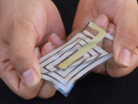
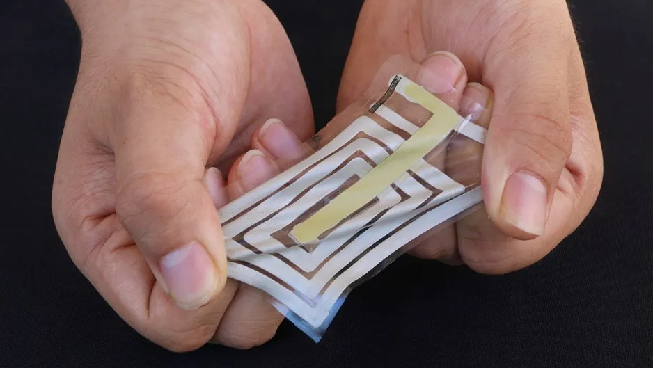
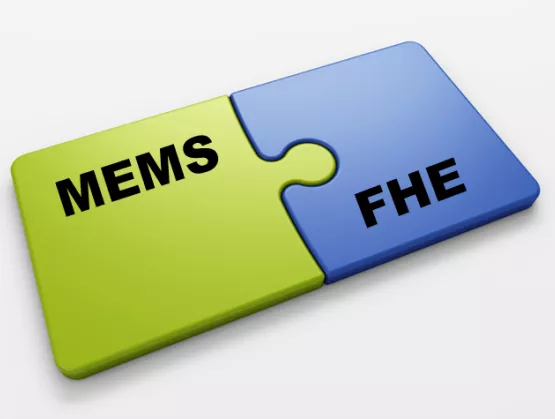
MEMS technology has changed human interaction with electronic devices. Introduced in the 1990s, the first mass-market MEMS devices were used for inkjet printheads and automotive airbag crash sensors. Today, MEMS are ubiquitous, with billions of the tiny devices adding intelligence and interactivity to smartphones, smart speakers, wearables, automobiles, biomedical devices, remote monitoring and event detection systems, and countless other applications. Integrating MEMS with Flexible Hybrid Electronics (FHE) is an important step in the evolution of this miniaturized intelligent sensing technology, paving the way for its use in new classes of flexible, conformal devices.The integration of the two technologies promises to breed new applications in small form factors but also presents challenges inherent to FHE design and fabrication processes. SEMI’s Nishita Rao caught up with Nathan Pretorius, prototyping and automation engineer, NextFlex, to discuss MEMS-FHE device integration challenges and opportunities ahead of his February 26 presentation, Integrating MEMS Devices in FHE, at FLEX|MEMS Sensors Technical Congress (MSTC) 2020, February 24-27, 2020, at the DoubleTree by Hilton in San Jose, California.Join us at FLEX|MSTC to meet Nathan and other industry influencers advancing innovation in FHE and MEMS sensors. Register now to connect with him at FLEX|MSTC or visit him on LinkedIn.SEMI: Why is integrating MEMS devices into FHE systems important? What new use cases might it enable?Pretorius: The main value proposition of integrating MEMS devices into FHE is that it allows MEMS devices to exist in a different form factor than was possible previously, giving us high-quality MEMS sensors on the flexible and conformable platform of FHE.Ease of application, flexibility, lower cost and rapid iteration on a design are just some of the benefits of FHE devices. And because there are few robust FHE sensors that overlap with MEMS’ capabilities, when you combine the two, you get a lot of compelling uses. That’s why NextFlex is working with agencies and companies to evaluate MEMS’ integration, including using bare MEMS die with microfluidics and promoting new ways of attaching and packaging MEMS die for use with FHE. SEMI: Why is FHE an ideal platform for integrating various types of sensors?Pretorius: MEMS integrated with FHE devices are ideal for rapid design and deployment of data-gathering sensor nodes — which we can iterate for specific applications. A few examples include on-body health monitoring devices for bio-fluids analysis, medical pressure sensors for monitoring blood pressure, and peel-and-stick sensors nodes for infrastructure monitoring. In terms of design and production, FHE devices support rapid prototyping, allowing for instantaneous design-iteration cycles. This speeds design-to-production over traditional rigid PCBs and copper flex because the feedback cycle time between design, manufacturing and testing is shorter, accelerating time to market. What’s exciting about FHE technology is that a variety of sensors or components, including MEMS, can be designed into the base system to easily customize it for a specific application. In addition, our experience shows that when compared to a traditional rigid PCB, an FHE board reduces manufacturing steps and device weight by two-thirds and, perhaps most importantly, converts the device to a thin, conformal shape that makes possible products in new form factors. SEMI: What are the primary challenges to integrating MEMS with FHE? What is NextFlex doing to help device manufacturers address these challenges? Pretorius: There are a few challenges, some of which are device-specific. Most recently, I’ve been focusing on inertial and timing devices, including accelerometers, gyroscopes and resonators. There are a few technical challenges involved in the process of getting the devices from the wafer to an FHE substrate. The wafer processing is very important, especially the dicing and thinning steps. After thinning and dicing, the die is placed onto the FHE substrate. The stresses caused by bonding to the substrate have to be understood and characterized. After placing the die, you then have a calibration step, which is normally performed after the device is packaged. With a MEMS die placed onto directly onto an FHE substrate, calibration then must be done.Finally, the device encapsulation is important, since on an FHE substrate the hard-to-soft material transition is very important to mitigate stresses to rigid component interfaces. We have also been looking at how to work with devices that have damping vents. Flexible encapsulants are inherently more permeable to gases and water vapor than hard encapsulants, so studying the encapsulation of MEMS devices on FHE is another area of interest. NextFlex has been working in a supporting role to evaluate best design practices and best attach and integration methods. In addition to our ongoing collaborative programs, NextFlex is developing the FHE manufacturing ecosystem to include system and component manufacturers and designers, product developers, and materials and equipment providers.SEMI: How do we facilitate closer collaboration between the FHE manufacturing ecosystem and MEMS suppliers such as MEMS device manufacturers, product developers, and materials and equipment providers?Pretorius: It’s important to include manufacturers early in the design process so we can identify challenges up front. That’s why NextFlex spearheads technology road-mapping efforts that include representatives from across the manufacturing ecosystem. We use the roadmaps to prioritize challenges that we can address effectively through collaboration, focusing the industry on solving problems through Project Calls that reveal integration challenges and results from real devices and that tell us how the materials and equipment actually perform with a real device.NextFlex keeps the information flowing, holding quarterly project update webinars to share results. As current devices are optimized for the process in which they will be used, we learn a lot from the project performers who make FHE system demonstrators — and we share that information with the member community. SEMI: Can you point to an example of a successful MEMS-FHE device integration?Pretorius: MEMS-FHE integration is still in the early stages, but we are working on several projects including a DARPA Seedling project for which we have integrated MEMS sensors into FHE systems for testing and evaluation. We plan to continue this work by integrating MEMS and FHE devices using methods that support mass production.SEMI: What would you like FLEX|MSTC attendees to take away from your presentation?Pretorius: We would like to see the FHE community work more closely with MEMS device manufacturers. For example, NextFlex often works with manufacturers to gain access to bare die, which is still a significant hurdle in making devices.The best way to speed things along is to get involved. We encourage FLEX|MSTC attendees to join NextFlex. As a prototyping and automation engineer at NextFlex, Nathan Pretorius explores new print methods for prototyping and automation using novel materials and processes. Pretorius currently focuses on how best to apply software scripting and machine learning to streamline FHE processes. Prior to joining NextFlex, he researched the strengths of roll to roll and screen printing on printed electronics designs, including capacitive touch interfaces, FHE passive component design, and antennas. Nathan holds a Bachelor of Science degree in Graphic Communications from Clemson University. FLEX|MSTC is organized MEMS Sensors Industry Group (MSIG) and FlexTech, SEMI technology communities focused on the growth of MEMS sensors and the flexible electronics supply chain, respectively.Nishita Rao is marketing manager for technology communities at SEMI.
Read More