downloadGroupGroupnoun_press release_995423_000000 copyGroupnoun_Feed_96767_000000Group 19noun_pictures_1817522_000000Member company iconResource item iconStore item iconGroup 19Group 19noun_Photo_2085192_000000 Copynoun_presentation_2096081_000000Group 19Group Copy 7noun_webinar_692730_000000Path
Skip to main content
Tensions between the U.S. and China have reached fever pitch as the Trump administration imposed higher tariffs on $200 billion of Chinese goods last Monday, adding to the $50 billion in goods hit with higher duties earlier this year. Bloomberg News reported that “the combined $250 billion in products facing levies is almost half the value of imports from China last year.”China countered by meting out stiffer tariffs on $60 billion in U.S. goods, on top of the $50 billion already levied, and canceling planned trade negotiations with the Trump administration.Days before the sharp escalation of the trade conflict, SEMI president and CEO Ajit Manocha joined SEMI China president Lung Chu in hosting a closed-door round table with 16 senior semiconductor industry executives in Shanghai. The goal: An update from the China semiconductor sector on its needs as the chip industry braces to weather the conflict. Manocha and Chu then met with influential China media outlets including Semiconductor Manufacturing, China Integrated Circuit, Silicon Semiconductor and IC Café to reiterate SEMI’s position on trade.“The basic principles of SEMI are free and fair trade, open markets, cooperation for mutual benefit, and protection of intellectual property rights,” Manocha told the reporters. “Tariffs and trade frictions are bound to harm the industry’s development.”Manocha highlighted efforts over the past few months by the SEMI advocacy team to educate U.S. policymakers on the impact of tariffs on the development of the semiconductor industry. Last month, the office of the U.S. Trade Representative (USTR) held a hearing in Washington, D.C. to solicit public comment on then-proposed tariffs on $200 billion of Chinese imports to the U.S. Testifying on behalf of the semiconductor industry, SEMI stressed that tariffs on more than 100 tariff lines covering items critical to semiconductor manufacturing “will harm companies in the semiconductor supply chain by increasing business costs, introducing uncertainty, and stifling innovation.” SEMI had testified twice before this year – the first time in May, opposing levies on $34 billion in Chinese goods, and the second in July to speak out against higher duties on $16 billion worth of Chinese products.SEMI China president Lung Chu made clear the consensus of China’s semiconductor sector: The trade war will profoundly impact the global semiconductor industry. He also stressed that SEMI, as a global industry organization linking the global electronic semiconductor industry chain, will continue to promote win-win cooperation between the U.S. and China.Manocha reaffirmed SEMI’s longstanding commitment to promote cooperation among nations and policies that foster industry growth.“For the growth of the semiconductor industry, SEMI is focused on four important factors, and we call them the 4 T’s, namely Tax, Technology, Talent, Trade,” Manocha told the media. “All are indispensable for the development of the industry.” SEMI president and CEO Ajit Manocha and SEMI China president Lung Chu host press conference in Shanghai.Because the semiconductor industry is international, with key features spread across a number of regions, cross-border cooperation is an eternal theme, Chu told the gathering. To maintain the vitality of China's semiconductor industry, the region must deepen its integration with the international semiconductor ecosphere. He acknowledged that there will be no quick answers to easing trade tensions between the U.S. and China but that SEMI would continue to press ahead in efforts to help improve relations. Despite the conflict, the industry remains optimistic about the growth of China’s semiconductor industry, he said."However, we need to face up to the fact that there is still a certain gap between the domestic semiconductor industry and that of international advanced level,” Lu said. “Therefore, international cooperation is the key to industry growth."Of the four cornerstones of the semiconductor industry – design, manufacturing, testing and equipment materials – China in recent years has narrowed the gap with its international counterparts in testing capabilities, Chu said. For China’s semiconductor industry to flower, the region must build strengths in design, manufacturing and materials too.“The semiconductor industry needs long-term investment, persistence and patience, and also needs win-win cooperation, continuous innovation and product applications across the entire industry,” Chu said. “Money is not the only incentive.”Manocha emphasized the theme of international cooperation, with the global semiconductor industry working in harmony.“The global semiconductor industry chain is inseparable, and each region has its own advantages,” Manocha said. “So, we will continue to work hard to create a win-win, inclusive global industrial atmosphere.”For its part, SEMI China is focused on becoming the best partner for China to realize its semiconductor dream by continuing to provide services that encourage international cooperation. That role will grow in importance with SEMI’s expansion into application areas such as smart manufacturing, smart transportation, smart data and smart automotive – all requiring tighter integration of the electronics industry supply chain.Cherry Sun is a marketing manager at SEMI China.
Read More
[caption id="attachment_12359" align="alignright" width="300"] (Courtesy: PRNewsfoto/QuickLogic Corporation)[/caption] Some great pieces of FD-SOI news from QuickLogic. The company recently demonstrated its ultra-low power ArcticPro™ embedded FPGA (eFPGA) solutions at the GlobalFoundries Technology Conferences in Santa Clara, California, Munich and Shanghai. The technology is available now. ArcticPro is the industry's first eFPGA offering for GF's 22FDX® process (btw they've been shipping it in volume for GF's 65nm and 40nm bulk processes for years). The company says its ultra-low power eFPGA architecture and mature software offer semiconductor and system companies the ability to integrate programmable hardware accelerators to lower power consumption and the flexibility to reconfigure a device's functionality in the field. [caption id="attachment_12360" align="alignleft" width="300"] (Image courtesy: QuickLogic)[/caption] QuickLogic has also announced that the technical university ETH Zurich will integrate QuickLogic's ArcticPro technology onto the university's PULP platform. PULP is a silicon-proven open-source parallel platform for ultra-low power computing created with the objective of delivering high compute bandwidth combined with high-energy efficiency. ETH will become the first licensee of eFPGA technology from QuickLogic on GF's 22FDX process node. They will develop an SoC integrating ETHZ's open-source RISC-V cores and eFPGA technology, enabling users to offload critical functions from the processor(s) and implement them in eFPGA fabric. This approach creates multiple hardware co-processors that increase system efficiency and performance while decreasing power consumption. "The main goal of the PULP program is to use a multi-disciplinary approach to achieve extremely high-power efficiency for computing applications," said QuickLogic CTO Dr. Timothy Saxe. "QuickLogic has a tremendous depth of experience in achieving low power consumption across a broad range of applications, including AI and IoT at the edge and security, and we look forward to contributing what we've learned along with our eFPGA technology to this groundbreaking initiative in low power computing." ETH's PULP platform with the fully integrated eFPGA is expected to be available Q1' 2019. QuickLogic is part of GF's fast-growing FDXcelerator™ partner ecosystem, offering customers ultra-low power (eFPGA) Intellectual Property, complete software tools and a compiler.
Read More
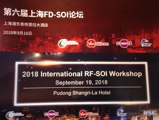
Excellent news and exciting applications made headlines at the recent FD-SOI and RF-SOI events in Shanghai. During the FD-SOI day, Amazon/Blink and Intellifusion shared news about their new chips, and we got updates from GF and Samsung. The RF-SOI day featured a great talk with details about China Mobile's 5G plans, and peeks at Nokia's groundbreaking approach and Qorvo's outlook. [caption id="attachment_12354" align="alignright" width="300"] (Photo courtesy: Verisilicon)[/caption] The hall was absolutely full – with over 300 people attending each day. The FD-SOI event was by invitation only, and there were far more people wanting to attend than there was room for, even given the big room in which the events were held. The events got excellent coverage in the China tech press. For example, EEWorld started with an overview article and added five supporting pieces zooming in on key presentations and companies: one on GlobalFoundries, one on Samsung, one on Verisilicon, and two on Soitec (CEO and top exec interviews). These pieces are in Chinese, but just open the links through your favorite translation site. Many of the key slides are captured in these articles, so if you can't wait for the ppts to be posted on the SOI Consortium website, you can get some quick previews now. The Verisilicon PR folks also wrote up highlights of the FD-SOI event in real time with lots of great pictures – you can read that here. Many thanks to that team, too, for flagging the coverage in the China press and posting it on their WeChat account. On the RF-SOI side, the Simgui folks wrote that up – you can read it here. They also sponsored a gala dinner with awards given to Qorvo and SmarterMicro – you can read about that here. Most of the presentations will be posted on the SOI Consortium website over the next few weeks, at which point we'll cover them in-depth here at ASN. But for now, here's a quick round-up of some of the highlights. FD-SOI Highlights [caption id="attachment_12347" align="alignright" width="300"] (Courtesy: Blink, Verisilicon)[/caption] Boston-area based Blink, which makes very popular home security systems, was recently bought by Amazon (see their current product page here). They just taped out a new chip on Samsung's 28FDS FD-SOI technology, and they're really happy about it. “I believe for battery powered devices at home, FD-SOI is the way to go,” said Yantoa Jia, Head of ASIC China Ops at Blink. Their goal in the move from 55nm bulk to 28nm FD-SOI was to double battery life, add features and control costs: and they did it. Even adding two more CPU cores and lots more features, “The power drop is fantastic,” he said. Design was no problem, he continued, and there was plenty of IP. Once the new generation is officially announced, he promised to sit down with ASN and give us more details. Attendees also heard about a new chipset from Intellifusion, which is putting its face recognition technology onto GlobalFoundries' 22FDX FD-SOI with design house Verisilicon. CEO Nin Chen gave an impromptu talk about how their technology is used to find missing people and property. The new chip, which is especially designed for use in cities, is network-to-cloud leveraging AI. For his part Thomas Morgenstern, GlobalFoundries SVP and GM of the Dresden Fab 1, said they're seeing high yields and increasing capacity for 22FDX. The marketing and manufacturing ecosystem has been built around the fab in Europe. Now, he said, the key is to build an FD-SOI ecosystem in China. The market needs of China largely parallel those of Europe, he noted, for performance and efficiency at the right cost point. The ecosystem enables fast time-to-market and 1st-time-right. [caption id="attachment_12343" align="alignleft" width="300"] (Photo courtesy: Cadence)[/caption] Samsung SVP Gitae Jeong sees their FD-SOI technology as the right solution for the 4th Revolution, which includes everything from energy harvesting to self-driving cars. They've just taped out their first 5G mmWave cellular chip on 28FDS, he revealed. eMRAM is looking very good, only requiring three additional masks and getting stable yields from -40o to 105oC. 18FDS is on schedule, with PDK 0.5 now being released, and 1.0 on track for release in March 2019. They expect a very fast ramp, and are looking at a 35% area reduction, power cut in half and performance up 22% compared to 28FDS. RF-SOI Highlights [caption id="attachment_12350" align="alignright" width="300"] China Mobile, Project Manager Danni Song (Photo courtesy: Simgui)[/caption] When China Mobile talks, the world listens. Project Manager Danni Song presented again this year (she gave a great talk last year, too). China has a very ambitious 5G project underway, and under two years in which to roll it out. The biggest challenges are power consumption and cost (a problem made worse by the additional power amplifiers needed for MIMO). Can RF-SOI help solve these challenges, she asked? One thing she did clarify during the panel discussion was with respect to the mmWave part of the 5G puzzle. Their initial 2020 rollout will only focus on sub-6GHz, with mmWave following a year or two later. Michael Reiha, Head of RFIC R D at Nokia Mobile Networks clarified the worldwide 5G rollout during the panel discussion. Different locations on the planet have different histories and needs, so will rollout 5G in different ways. For historical reasons (and a lack of choice), the US will lead with mmWave, he said. Europe, meanwhile, will focus on 24GHz to meet the needs of automotive radar. In his presentation, Reiha described Nokia's approach to power amplifiers (PA), which is very different from what others are doing. With RF-SOI, he said, you can add sensors and logic for a level of preventative care, so you can gauge and protect your equipment using AI. He believes this disruptive approach will put them two years ahead of the industry, enabling massive MIMO to be deployed in dense urban areas with 60% lower power consumption and 50% savings in material costs. Go read about their Reefshark tech, he urged, which he says will beat GaAs. “The future is very bright with RF-SOI,” he concluded. “I can state that with confidence.” [caption id="attachment_12351" align="alignleft" width="300"] Julio Costa, Director of Technology Development, Qorvo (Photo courtesy: Simgui)[/caption] Julio Costa, Director of Technology Development at Qorvo sees it differently. Traditionally a GaAs house, all their RF-SOI work is fabless. While RF front end modules (FEMs) are loaded with RF-SOI, he said, and are a big winner for antenna tuning, Qorvo still sees GaAs for high-efficiency amplifiers and envelope tracking. But, he said, it will be a battle. GaAs wins in terms of area and power consumption he contends, but adds that SOI wins in terms of cost. Power levels, he predicts, will be the determining factor. So that's the quick overview – we'll drill down into the presentations as they're posted, so stay tuned!
Read More
Outsourced Semiconductor Assembly and Test (OSAT) service providers experienced strong growth in 2017, but will this growth continue? In the last few years, OSAT growth has been driven by shipments for packages found in smartphones, but this market is slowing. What will replace it? Growth in power devices is strong and electronic content in vehicles is increasing. Will OSATs participate in this growth? Many OSATs have plants dedicated to automotive package assembly and will see continued growth. Growing demand for connectivity everywhere, called IoT, is generating large amounts of data, creating the need for more servers and datacenters. The adoption of Artificial Intelligence (AI) across a broad range of applications is driving demand for high-performance packages, but will this assembly take place at the OSATs or foundries? In the third and fourth quarters of 2017, growth in cryptocurrency provided unanticipated revenue for a number of OSATs. Given that the most well-known crypto mining companies and the biggest mining pools are all based in China, several OSATs, including major Taiwanese and Chinese service providers, experienced revenue growth in 2017 directly attributed to the assembly of ASICs in flip chip scale packages (FC-CSPs) and GPUs in flip chip ball grid arrays (FC-BGAs) for the cryptocurrency market. However, the first and second quarter of this year has seen decreased demand for GPUs and ASICs for this application. The assembly of packages for cryptocurrency slowed considerably in the first half of the year and therefore can’t be counted on to add as much to the revenue base as in the previous year. Going into the latter half of the year, the demand for Crypto ASICs is expected to pick up as new generation of 7nm chips will drive new investment and replacement cycle while crypto-mining GPU will see a further decline. Three of the top 10 OSATs, Jiangsu Changjiang Electronics Technology (JCET), Tianshui Huatian Technology (Huatian), and Tongfu Microelectronics (TFME), are based in China. China’s share of the top 10 OSATs’ revenue increased from slightly less than 23 percent in 2016 to more than 25 percent in 2017, and this trend is expected to continue. Crypto-related packaging and test business has certainly contributed a big portion of the share gain. Major OSATs such as TFME and Tianshui Huatian plan expansion in their plants and they expect to fill this added capacity in a broad range of packages. Huatian’s new Nanjing plant will include assembly for memory packages. TFME plans to set up a plant in Xiamen, Fujian Province to provide bumping, wafer level packaging, and system-in-packaging (SiP) services. Tracking the capabilities of OSATs is increasingly important. SEMI and TechSearch International have introduced a new Worldwide OSAT Manufacturing Site Database that provides listings of OSAT facility locations and package and test options in each factory. This database indicates the specific packages offered at each location. Finding plants that offer automotive qualified assembly is also possible with the database. Companies that offer bumping and wafer level packaging are identified. Over 120 companies and 300 facilities are tracked in this database covering both OSAT packaging and test facilities. For additional information about this informative database, please visit https://discover.semi.org/osat-database-registration.html E. Jan Vardaman is president of TechSearch International, Inc., and Clark Tseng is director of Industry Research and Statistics at SEMI.
Read More
With one of the oldest and largest public education systems in the developed world, how well does the US public education system serve the global electronics industry? Public education in the US has had time on its side. In 1635 the Boston Latin School became the first public school in the US. Boston Latin was originally a boys-only secondary school that taught Greek, Latin and the humanities. It wasn’t until 1918, however, that the US government required all children to obtain at least an elementary-school education – available to them through free public schools. As public education increasingly served the masses rather than just the elite, a balance of humanities, mathematics and science began to replace the classics.While free public education in the US got a comparatively early start, most American students score lower in science and math than students in many other developed nations. According to a 2017 Pew Research Study, 15-year-old American students ranked 24th in the world in international standardized age-group science testing and 38th in the world in standardized mathematics testing. While test scores are just one measure of proficiency, do they in some way reflect a lack of motivation to study science and math because of students’ unfamiliarity with STEM careers? Source: Pew Research. See article. Make STEM RelevantIf we want the US to remain a leader in the global electronics industry, we need to pay attention to the disconnects between academics and workforce development. We must help show students at an early age that STEM careers can be exciting, creative and fulfilling, and that math and science are essential to STEM.Ways to Get InvolvedWhether you work for a large publicly traded electronics manufacturer, an equipment or materials supplier, a foundry or a startup, you can take action to support student engagement in STEM. Here are a few ways to get involved:Participate in Community Programs One fun way to inspire budding technologists is to sponsor one of the FIRST programs for students. These age-segmented competitive programs range from FIRST LEGO League, Jr. Challenge for six-ten year-olds to FIRST Robotics Challenges for high school and college students, giving you the opportunity to sponsor a team or even to coach.Our company sponsors Team TNT, a Southern Oregon-based team that placed among the world’s top high school robotics teams at the spring 2018 world championships. We also brought two members of Team TNT to SEMICON West 2018, where they attended SEMI’s three-day High Tech U and presented their insights on building their FIRST Challenge robot at the Smart Workforce Pavilion. Margaux Quady (L) and Matthew Mills (R), Team TNT members, presented at SEMI’s Smart Workforce Pavilion at SEMICON West (Rogue Valley Microdevices) Concerned about the dearth of girls interested in STEM — and the small numbers of women in engineering careers? Look for your local equivalent of the Advocates for Women in Science, Engineering, and Math (AWSEM) Symposium, a day-long program for middle school girls. One of our engineers, Jennifer Devin, gave a hands-on workshop on deconstructing smartphones to showcase the silicon chips inside them. If you cannot find something like AWSEM, check out national programs such as the Society for Women Engineers (SWE)’s SWENext program for girls ages 13-18 as well as Girl Powered.Partner with Local SchoolsYou would be surprised at the opportunities to present what you do in the classrooms of school-age children. Take after Allyson Hartzell, managing engineer at Veryst Engineering in Needham, MA. Allyson speaks with students in her local elementary schools of Somerville and Cambridge, Massachusetts because she thinks that we must reach younger children to get them excited about STEM learning. “Waiting until middle school or high school to help students visualize the real-world appeal of STEM careers is just too late,” said Hartzell. “I’ve had amazing experiences working with local elementary-school students. Students become engaged when you show them real-world examples such as electron micrographs of MEMS.”Many middle schools and high schools also look to their communities to provide tutors in STEM subjects. Check with the community liaison at your local school to get started.Engage in Internship ProgramsInvolvement doesn’t stop in the K-12 grades. Seek out a local university’s internship program and hire some interns in that program to work at your company. The interns will gain valuable applied experience in your environment, and you might find young engineers who would love to join your company after they graduate. Oregon’s MECOP, an engineering-specific internship program founded on close industry-university collaboration, has been amazing for our recruitment. Some of our finest engineers were once in the MECOP program, including our engineering manager.Anything you do to get involved in inspiring coming generations of students to explore STEM — no matter how small your action — will make a positive difference in helping US students become better prepared to enter a technology-focused workforce. Through collaboration and creativity, we can help US companies keep the global electronics industry moving toward greater innovation. Jessica Gomez, CEO and co-founder of Rogue Valley Microdevices, entered the semiconductor manufacturing field in 1998 at Standard Microsystems Corporation of Hauppauge, New York where she acquired valuable knowledge in both semiconductor processing and production management. Jessica also held positions at Integrated Micromachines and Xponent Photonics prior to co-founding Rogue Valley Microdevices in 2003. As head of a technology company, Jessica recognizes the criticality of workforce development – and has become an advocate of STEM education. Rogue Valley Microdevices supports STEM initiatives for middle-school girls, a competitive robotics team for high school students, and a college internship program specifically for engineers.Expanding her energies beyond the company she co-founded, Jessica is also applying her passion for change to politics. She is currently campaigning for the Oregon State Senate.For more information, visit Rogue Valley Microdevices.
Read More
Over the last three years the number of battery-operated electronic-component solutions for the Internet of Things (IoT) and Industrial IoT (IIoT) applications has been increasing steadily. This trend will continue for years to come, particularly with the growing popularity of mobile devices of all flavors. Addressing power consumption for battery-powered always-on IoT/IIoT devices – which rely on dozens of electronic components, including sensors — is critical to their commercial success.The demand for ultra-low-power sensors has accelerated the race to squeeze every last mW from components. Compared to previous-generations of sensors, semiconductor suppliers have managed to drastically reduce power by as much as 50%-60% over older solutions. Leveraging new state-of-the-art analog design techniques, we have effectively optimized capacitive readings of MEMS structures. How effective are they? We estimate that with the right mix of our company’s power-saving technologies, it is possible our customers could save 3MW/year globally[1].What’s next?While the semiconductor industry continues to investigate novel technologies, approaches and analog IP for greater energy efficiency, we believe that bigger gains in reducing power consumption will come from thinking at the system level. The sensor node is a good place to start.A typical IoT node is composed of a set of sensors, a microcontroller, a radio frequency (RF) link, and a power-supply system, often based on Li-Po batteries.Of these, the microcontroller and RF link consume the most energy and, in the RF link, power consumption is a function of the distance between end point and receiver and of the amount of data transmitted. Thus, at longer distances reducing the amount of data transmitted can save power. We can achieve this by including some pre-elaboration capabilities on-board and by extracting more meaningful information from the raw sensor data.We address this by moving some computation and data analysis inside the sensors, where smart hardware “digital blocks” perform faster and more efficiently than software-based routines running in the microcontroller. We can achieve this by using dedicated hardware resources to reduce overall system power consumption. The beauty of this solution is that it allows the microcontroller to operate in low-power states by only transmitting significant information in batches. The SensorTile development kit can speed up prototyping of ultra-low-power IoT devices by integrating an ultra-low-power MCU and BlueNRG Bluetooth radio with sensors. Some examples of these advanced digital blocks are the Advanced Embedded Pedometer, the Finite State Machine and Decision Tree, and Compressed FIFO in an IMU.The Advanced Embedded Pedometer is a hard-wired step counter that works independently inside the sensor, without CPU intervention: By comparing sensor outputs to pre-defined and -loaded patterns, it autonomously decides whether the user is walking or running to start and stop counting the user’s steps. The sensor then makes this information available to the microprocessor for further elaboration or for simple notification to the user.The Finite State Machine and Decision Tree are new functions dedicated to pattern recognition (machine learning) and decision-making: They can perform complex classifications and state detection, and can send dedicated warning and signaling to the microprocessor. A good real-world example is industrial predictive maintenance, where the sensor can categorize and identify different malfunctioning states in the equipment before waking the microprocessor to react.Our products, on average, save about 1 mA (1e-3) over competitive devices or over our previous-generation parts. So 2.0 x 1e-3 x 1.5e9 = 3MW. Programmable Sensor and Decision Tree Finite State Machine Integrating programmable sensors and decision trees as well as finite state machines in the sensor allows the sensor to do more of the work while the MCU sleeps. Source: STMicroelectronics Another example is compressed FIFO (first-in, first-out) buffer, which can store sensor data in the sensor, not in raw format, by using efficient compression algorithms. In addition to saving memory (and therefore silicon area) inside the sensor chip, it also saves power by reducing the number of bytes transferred to the processor and by shortening the communication data flow, which reduces processor-active time.These examples – the Advanced Embedded Pedometer, the Finite State Machine and Decision Tree, and compressed FIFO buffer – are just some showing that we can develop low-power IoT/IIoT devices through intelligent management of sensors, microcontrollers and other components in any given system. Your starting point is an IoT/IIoT node that lets you selectively allocate some power-hungry tasks — such as computation and data analysis — to sensors instead of the microcontroller. Leveraging data blocks that reside in the sensors alleviates the microcontroller’s typical power drain, allowing the microcontroller to operate with maximum efficiency.[1] ST sells about 1.5 billion pieces/year (1.5e9), which typically run from a 2V supply. Luca Fontanella joined ST Microsystems in 1995 as an analog designer. In 2001 he joined the MEMS team in a marketing role and today he is marketing manager in the MEMS Sensor Division. Luca has contributed to 25+ international patents and has presented at multiple conferences. He earned a degree in Electronic Engineering from Padua University. Simone Ferri joined STMicroelectronics in 1999 as Central R D engineer, moved to the Audio Division as a digital designer and is now director of the Consumer MEMS Business Unit. He holds a degree in Electronic Engineering and an MBA from the Polytechnic of Milan. _______________________________________________________________________________________________Brush up on the latest MEMS and sensors trends and gain a new perspective on emerging applications. Register today!
Read More
U.S. Government Imposes Tariffs on $200 Billion of Goods and China Retaliates on $60 Billion of GoodsEarlier this week, the U.S. Trade Representative (USTR) released a 10 percent tariff on $200 billion in imports from China, including more than 90 tariff lines central to the semiconductor industry.The 10 percent tariff will take effect on September 24, 2018, and rise to 25 percent on January 1. These tariff lines will cost SEMI’s 400 U.S. members tens of millions of dollars annually in additional duties. However, counting the products included in the previous rounds of tariffs, the total estimated impact exceeds $700 million annually. China has already announced that it will respond with tariffs on $60 billion worth of U.S. goods. In his notice, President Trump said the U.S. will impose tariffs on $267 billion worth of goods if China retaliates. The U.S. government removed 279 total tariff lines, including three lines that impact our industry: silicon carbide, tungsten, and network hubs used in the manufacturing process.As we’ve noted, intellectual property is critical to the semiconductor industry, and SEMI strongly supports efforts to better protect valuable IP. However, we believe that these tariffs will ultimately do nothing to address the concerns with China’s trade practices. This sledgehammer approach will introduce significant uncertainty, impose greater costs, and potentially lead to a trade war. This undue harm will ultimately undercut our companies’ ability to sell overseas, which will only stifle innovation and curb U.S. technological leadership.Product Exclusion Process – List 2USTR formally published the details for the product exclusion process for products subject to the List 2 China 301 tariffs (the $16 billion tariff list). If your company’s products are subject to tariffs, you can request an exclusion.In evaluating product exclusion requests, the USTR will consider whether a product is available from a source outside of China, whether the additional duties would cause severe economic harm to the requestor or other U.S. interests, and whether the product is strategically important or related to Chinese industrial programs (such as “Made in China 2025”).The request period ends on December 18, 2018, and approved exclusions will be effective for one year, applying retroactively to August 23, 2018. Because exclusions will be made on a product basis, a particular exclusion will apply to all imports of the product, regardless of whether the importer filed a request.More information, including the process for submitting the product exclusion request and details what information should be included in your submission can be found here. Please let me know if your company plans on filing an exclusion. SEMI has prepared a document that includes guidelines for your exclusion filing, an explainer on how to submit, and links to official government info. SEMI is glad to assist your companies file exclusion requests for your products. SEMI will continue tracking ongoing trade developments. Any SEMI members with questions should contact Jay Chittooran, Public Policy Manager at SEMI, at [email protected].
Read More
SEMI FabView update for calendar year Q3 2018 Global fab construction investment shows continuing strength, with 19 new fab projects expected to begin construction in 2019 and 2020, based on the latest data published in SEMI’s World Fab Forecast. Fab investment is just one indicator of how growing demand in areas such as high-performance computing, data storage, artificial intelligence (AI), cloud computing, and automotive are driving the fourth consecutive year of spending growth in the semiconductor industry. Below are a few highlights* from September’s SEMI FabView: Memory: Not fading Micron plans to invest $3 billion by 2030 in Manassas, Virginia – These investments, driven by strong demand for automotive applications, are contemplated in Micron's long-term model. The production ramp is anticipated to be in the first half of 2020. SK Hynix to build new DRAM fab in Icheon (Gyeonggi Province), Korea – The construction, to be completed by the end of 2020, will adopt 1znm node (probably EUV). Total investment is estimated to exceed $13 billion. Nanya Technology doubles 2018 capex plan – The increase is for additional DRAM capacity and more 20nm DRAM conversion (from 30nm). 200mm and below: Not leading edge, but continues to draw investment Vanguard changes fab investment strategy – Vanguard will focus on 200 mm and has scrapped its plan for 300mm expansion. Murata to invest into 150mm expansion – Murata announced a 5 billion Yen investment (US$44.6 million) in a new fab extension in Vantaa, Finland. Investment, M A in Analog, Logic, Power and Opto Segments Texas Instruments is looking to invest $3.2 billion in new fab construction in 2019 – Texas Instruments is eyeing Richardson, Texas and also considering sites outside Texas. Bosch 300mm fab in Dresden, Germany – Bosch held a groundbreaking ceremony on April 24. Equipment installation is expected in 2H19. Microchip completes acquisition of Microsemi – Microchip closed its $8.45 billion acquisition of Microsemi on May 29. Microsemi has five fabs in the U.S. with a wide range of semiconductor products and system solutions. New fabs in China keep on coming Shanghai Jita Semiconductor/Huada Semiconductor – Shanghai Jita Semiconductor, a subsidiary of Huada Semiconductor and China Electronics Corporation (CEC), announced plans earlier this month to build both 200 mm and 300 mm semiconductor fabs for analog and power semiconductors in Shanghai. The combined fab investment will total $5.18 billion. Hamamatsu Photonics building 200 mm fab – Hamamatsu announced that it is building a new facility Investment of 2.8 billion Yen (US$25 million) to boost opto semiconductor capacity. Production is anticipated to start in late 2019. * Actual FabView updates provide more detail SEMI FabView, a mobile-friendly, interactive version of SEMI’s popular World Fab Forecast, delivers on-demand fab information such as fab spending and capacity for over 1,200 facilities, including over 60 planned facilities worldwide, across a wide range of product segments including Power, GPU, Memory, Foundry, MEMS and Sensors fabs. Fab data include region, start of construction, operation, construction and equipment spending, capacity, wafer sizes, product types and geometries. SEMI FabView subscribers receive forecast model updates through SEMI’s World Fab Database. Click here for a trial if you want to experience SEMI FabView first hand. Christian G. Dieseldorff is senior principal analyst and Eugenia Liu is senior product marketing manager, Industry Research and Statistics, SEMI, Milpitas, California.
Read More
Materials innovation has always been vital to the semiconductor industry. In the past, it was high-κ gate dielectrics. Today, Cobalt is seen as a replacement for Tungsten in middle-of-line (MOL) contacts.What materials innovation will the future bring?A likely answer is Graphene, the wonder material discovered in 2004.Graphene is one atomic layer of carbon, the thinnest and strongest material that has ever existed. It is 200 times stronger than steel and the lightest material known to man (1 square meter weighing around 0.77 mg). It is an excellent electrical and thermal conductor at room temperature with an electron mobility of ~ 200,000cm2.V-1.s-1. At one atomic layer, graphene is flexible and transparent. Other notable properties of Graphene are its uniform absorption of light across the visible and near infrared spectrum and its applicability towards spintronics-based devices.Graphene and Moore’s LawMoore’s Law scaling can be broken down into 4 key areas: Lithography FET Advanced Packaging (2.5D and 3D IC) Interconnect Material Solutions for upcoming nodes are starting to emerge in the first two areas (EUV and Nanowire- or Nanosheet-based FET respectively). Graphene play an important role in the latter two areas. For advanced packaging, Graphene can be used as a heat spreader (to lower overall thermal resistance), or as an EM shield (to lower crosstalk) as part of a 3D IC package.Active Graphene device layers can potentially be stacked on top of each other using a low-temperature transfer process ( 400°C) to allow for a dense heterogeneous “memory near compute” configuration. This is an area DARPA is actively researching as part of its new $1.5 billion Electronics Resurgence Initiative.Regarding interconnects, Copper interconnects are running out of steam and becoming a major IC bottleneck (projected 40% total delay for 7 nm node). Graphene’s high electron mobility and thermal conductivity make it an attractive interconnect material for MOL and back-end-of-line (BEOL), especially at line widths 30 nm.Graphene Device ApplicationsGraphene-based semiconductor applications are already starting to hit the market. A fully integrated optical transceiver (with a Graphene modulator and photodetector) operating at 25 Gb/s/channel was on display at the recent Mobile World Congress in Barcelona. San Diego-based Nanomedical Diagnostics is selling a medical device that uses a Graphene biosensor. Europe-based Emberion is building Graphene optoelectronic sensors that might find a home in LIDAR applications, where there is currently a focus on improving sensing in low-light conditions.What will the overall Graphene roadmap in the semiconductor industry look like? The history of ion implantation serves as a good example of how a fundamental scientific discovery moves from the lab to the foundry floor.The dominant view in the semiconductor industry at the time was that ion implantation would not work in practice (vs. thermal diffusion) and that, if it did, it would only marginally improve the manufacturing yields of existing products. There was nothing obvious about the transfer of ion bombardment techniques from nuclear physics research to semiconductor production.Varian (led by British physicist Peter Rose) built a new, advanced ion implant tool that Mostek (DRAM manufacturer based in Texas) was able to use to create MOS ICs with clear competitive advantages. The successful collaboration between Varian and Mostek was the turning point in the development of ion implantation as a major semiconductor manufacturing process. Over the next few years, semiconductor firms used ion implantation in a growing number of process steps and, by the late 1970s, it became one of the main processes used in semiconductor manufacturing.Likewise, the Graphene world needs to work closely with the semiconductor industry to develop the tools and techniques required to solve fundamental issues around Graphene growth (good uniformity over large area, low defect density) and Graphene transfer (high throughput, CMOS compatible). It is only then will we fully realize a future that includes 2D materials.The first step in this process is cross-industry education and initiating the dialogue between semiconductor industry and graphene companies. The National Graphene Association will be hosting the largest gathering of graphene companies and commercial stakeholders at the Global Graphene Expo Conference, October 15-17, 2018, in Austin, Texas.Learn more about graphene at the upcoming Global Graphene Expo Conference with dedicated panels of experts and investors, and roundtable discussions on how Graphene will impact the semiconductor industry. The event promo code is SEMINGA. About the AuthorAnand Chamarthy is the CEO and Co-Founder of Lab 91, an Austin-based startup that is working towards Graphene/CMOS integration at the foundry level. Anand can be reached at [email protected]. About the National Graphene AssociationThe National Graphene Association is the main organization and body in the U.S. promoting and advocating for commercialization of graphene and addressing critical issues such as standards and policy development.
Read More
Last week, more than a dozen senior semiconductor executives traveled to Washington, DC for the first-ever Fall Washington Forum. The SEMI Washington Forum, a venue for SEMI members to educate lawmakers about the industry, focused on action against China, both in the form of tariffs and export controls.Our industry is global, and companies rely heavily on trade. In 2017, more than 90 percent of equipment made in the United States was exported. Because of this dynamic, the United States holds a nearly $9 billion trade surplus in this industry. SEMI supports trade policies that open foreign markets. In the meetings, the executives expressed deep concern that the tariffs would inflict deep damage to the U.S. economy, including to SEMI members. Estimates suggest that the Sec. 301 tariffs (and the Chinese retaliatory tariffs) will cost semiconductor companies more than $700 million annually, dramatically increasing the cost of doing business. These tariffs also threaten U.S. technological leadership. The United States has led innovation for decades. However, by pursuing policies that limit market access opportunities, company-led R D and innovation will slow, which, in turn, will curb further export potential. SEMI companies also stressed that because of the blunt application of these tariffs, this action will actually hurt U.S. companies as much as it hurts their Chinese competitors. Indeed, about 40 percent of imports in our sector from China are from U.S. or other non-Chinese companies. Further, the semiconductor industry relies on a vast network of supply chains, which have been built and qualified over the course of years. A fundamental revamp of supply chains is simply not feasible. This would be expensive, time-consuming, and resource-intensive. With a growing number of policy issues that are central to and could have significant impact for semiconductor companies, SEMI hosted its first ever Fall Washington Forum for members of its North American Advisory Board (NAAB). SEMI also invited several other industry executives. In total, 14 senior industry executives, including representatives from equipment manufacturers, component suppliers, and materials providers, attended the Fall ForumDuring the two days of meetings, SEMI met with several senior Administration officials to better the policies being enacted and considered as well as encourage all parties to not impose barriers to commerce, which would severely impact the semiconductor industry. SEMI also met with Members of Congress and their staffs on this issue. All told, attendees at the Fall Forum had more than 15 meetings with policymakers, reflecting the great impact of public policy on SEMI members companies. At a time when the stakes for the industry could not be higher, direct engagement with lawmakers is critical. The Washington Forum offers an incredible opportunity for members to better understand the impact of key public policy issues and gain firsthand experience in influencing policy and helping lawmakers better understand the industry.If you are interested in learning more about the SEMI Washington Forum or SEMI’s public policy program, please contact Jay Chittooran by email at [email protected].
Read More