downloadGroupGroupnoun_press release_995423_000000 copyGroupnoun_Feed_96767_000000Group 19noun_pictures_1817522_000000Member company iconResource item iconStore item iconGroup 19Group 19noun_Photo_2085192_000000 Copynoun_presentation_2096081_000000Group 19Group Copy 7noun_webinar_692730_000000Path
Skip to main content
Five young dancers bathed in a striking rainbow of colors with their silhouettes cast in the background dazzled SEMICON Japan 2018 attendees at the opening ceremony in mid-December. Gone were the standard opening keynotes and ribbon cutting, replaced by live performance and media art set against a dramatic black backdrop. There was no mistaking the wide-eyed looks of wonder in the audience.In its sheer vibrance, the opening ceremony thrilled with an excitement that seemed to embody the extraordinary growth expectations for the global semiconductor supply chain over the next five years, with the industry poised to double sales from $2 trillion to a staggering $4 trillion – a phenomena SEMI president and CEO Ajit Manocha has called The Rebirth of the Semiconductor Industry. Driving this unprecedented growth will be SMART applications that are transforming industries and applications worldwide, powered by artificial intelligence (AI) and Internet of Things (IoT) technologies.The dramatic scene at SEMICON Japan 2018 was staged by Rhizomatiks, a media arts company that produced the Rio Olympic Games closing ceremony and is famous for its pop music spectacles. The company’s CTO, Motoi Ishibashi, the event’s first keynote speaker, described his team’s development of drones and vehicles guided by motion and precision-control technologies. It was some of these SMART vehicles that maneuvered the opening ceremony performers from the dance company Elevenplay onstage. Only Rhizomatiks, Ishibashi said, has this capability. In its mission to enrich people’s lives through new media arts, Rhizomatiks uses the latest virtual and mixed-reality technologies to orchestrate not only dance performances but music videos, commercials, fashion shows and festivals.Toru Nishikawa, the second keynote speaker and CEO at Preferred Networks, a leading Japan-based developer of deep learning software programs, surprised the SEMICON Japan audience with his discussion of his company’s work to develop a specialized chip for deep learning processing, joining technology giants Apple, Google, Alibaba and Microsoft in chip design. As more IT and software companies develop specialized, differentiated chips, the devices are quickly becoming the heartbeat of SMART technologies. The company’s approach has taken hold. Only four years old, Preferred Networks is enjoying rapid growth by working with global powerhouses including Toyota, NTT, Panasonic, Fanuc, NVIDIA, Intel and Microsoft. Ishibashi’s and Nishikawa’s fresh visions and the media arts extravaganza reflected the success of SEMICON Japan, held again at Tokyo Big Sight: The event’s 1,881 booths – filled by 727 exhibitors from 14 regions – was the highest count in six years. With Japan home to companies that supply about 40 percent of semiconductor equipment and materials worldwide, top suppliers historically have occupied the largest spaces on the SEMICON Japan show floor.According to IDC, personal computers and smartphones, long the largest revenue sources for the semiconductor industry, will remain top revenue drivers in the coming years. But revenue from new SMART technologies for applications such as automotive and factory automation is growing, a trend expected to continue with a 2018-2022 CAGR of 9.5 percent for automotive and 5.2 percent for manufacturing, compared to 1.1 percent for PCs and 2.9 percent for smartphones.SEMICON Japan’s new SMART Applications zone highlighted these and other new market opportunities for semiconductor growth with product and technology exhibits from companies including Bosch, IBM, Microsoft, NEC, Preferred Networks, Sony, SAS, Siemens, Tesla and Toyota. But the zone wasn’t all work and no play. The ROBOT SQUARE and SPORTS x IOT robot exhibits took visitors back to their school days, with robot anime – from Astro Boy to Gundam and Evangelion – that they could ride and control! As the World Gets Smarter, So Must SEMICON and the IndustryWe all agree the world is getting smarter at a fast pace. New cars are easier to drive – some models are almost fully autonomous on highways and streets. Your SMART speaker has gone well beyond an audio playback device and is more like a home AI platform. Almost all storefronts are equipped with video cameras. Your workplace, whether an office or a factory, is driven by automation. The reliance of these environments and devices on semiconductors is driving exponential chip and changing the world. Businesses need to adapt and so do SEMICON events. We’re doing just that as SEMICON Japan 2018 demonstrated – from an opening ceremony enabled by technology innovation to new faces of the industry to the SMART Application zone. As the SEMICON Japan presidents’ reception concluded the first day of the show, a robot from the ROBOT SQUARE suddenly appeared in the reception hall in front of about 250 executives from the global industry. Everyone at the reception was impressed and stepped forward to the stage, reflecting the overall excitement about SEMICON Japan, which for many years showcased only chip manufacturing equipment and materials. This year, to keep pace with the changing world, it was much more than that.SEMICON Japan 2019 will again take place in December at Tokyo Big Sight. However, organizers of the Tokyo Olympics will be using the East Exhibit Hall usually occupied by SEMICON Japan to prepare for the games. As a result, SEMICON Japan will be held in the West and South Halls instead. Look for more changes to the event. I hope to see you next year!Jim Hamajima is president of SEMI Japan.
Read More
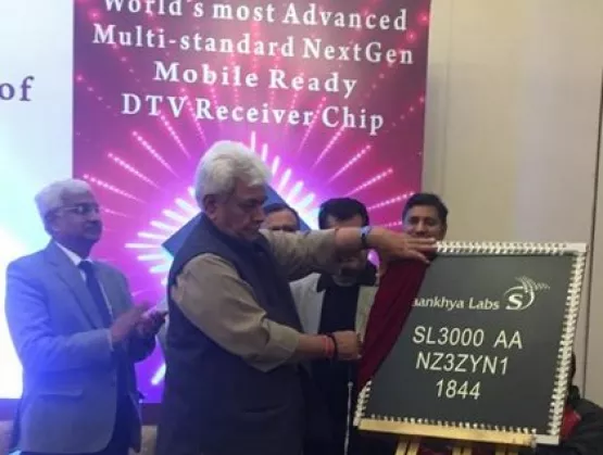
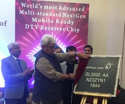
Going to CES? Check out the demo by Saankhya Labs. They just announced the launch of their latest next-gen digital terrestrial TV demodulator chipsets, SL3000 and SL4000. As reported by The Times of India and many other media outlets, the chipset is part of the Pruthvi-3 series, and it's being manufactured on Samsung Foundry's 28nm FD-SOI technology. Saankhya Labs says they'll be sampling in the 1st Quarter of 2019. [UPDATE 9 January 2019: Per a press release issued at CES, the chipset was launched by ONE Media 3.0, LLC, a subsidiary of Sinclair Broadcast Group, and Saankhya Labs in collaboration with VeriSilicon and Samsung Foundry. This announcement follows Sinclair Broadcast Group’s recent commitment to a nationwide roll-out of ATSC 3.0 ("Next Gen TV") service and its past announcement to fund millions of chipsets giveaways for wireless operators. Sinclair is a major TV station operator in the US. The PR goes on to say that the demodulator SoC was designed and developed by Saankhya Labs with ASIC turnkey design and manufacturing services from VeriSilicon, using Samsung Foundry’s state of the art 28FDS (its Fully Depleted SOI process technology), chosen for its unique low power capabilities offered by the back bias option.] [caption id="attachment_13581" align="alignright" width="300"] (Courtesy: @SaankhyaLabs)[/caption] The Pruthvi-3 is an upgrade of Saankyha's Software Defined Radio (SDR) chipsets for Direct to Mobile (DTM) applications, which address video bandwidth congestion and other challenges, including internet access for the vast populations of rural users found in India and worldwide. (DYK half the world still lacks access!?) The company says the SL300x will be the industry’s first SDR-based DTV Demodulator that supports all the leading broadcast terrestrial, cable and satellite TV standards including the ATSC 3.0. The SOC is designed to deliver high performance and high throughput in static and multipath environments. A power-efficient, small footprint device, it targets DTV receiver applications such as digital televisions, set top boxes, home theatres and automotive entertainment systems. The SL400x – for mobile phones and tablets – is designed to be the most technologically advanced and highly-integrated single chip Mobile DTV Receiver in the industry. The full featured front-end SOC integrates UHF RF tuner, baseband DTV demodulator, FEC decoder, de-interleaver memory and Analog to Digital Converter (ADC) in a single chip. Here is a brief YouTube video of the company's CEO at the launch event, explaining why they see this chipset as a game changer. India Times reports that there are already 5 million of the chipsets in pre-order to companies in the US and China.
Read More
4 Key Takeaways from SEMI Taiwan Member ForumThe rapid development of artificial intelligence (AI) has accelerated the digital transformation in various industries and has now fused with Internet of Things (IoT) to exploit the value of both technologies in reshaping the electronics industry value chain. As it emerges from the shadows of its parent technologies, AIoT is giving rise to new opportunities in manufacturing, healthcare, transportation, and even energy. AIoT is fast rising in prominence as an enabler of key electronics manufacturing process improvements and the creation of add-on value to existing products – both critical to the success of many businesses.SEMI and the SEMI MEMS Sensors Industry Group (SEMI-MSIG) held a technical forum on smart sensing and its applications in AI and AIoT, inviting renowned experts in sensors and edge computing to share in-depth insights into the latest AIoT technologies and applications with more than 100 industry professionals in research and development, marketing and sales. Here are four key takeaways from the SEMI Taiwan member forum.1. Steady Growth for Global Sensors MarketThe global sensors market’s steady growth is expected to expand at a CAGR of 6.6 percent from 2017 to 2023, with Asia driving the biggest gains and automotive leading the segments – including healthcare and education – with the strongest growth. Automotive alone is expected to reach US$34 billion in 2023.2. Integration Critical to MEMS Sensors DesignsWith AI booming, MEMS sensor designs need to drive toward greater integration —not only integrating data collection with sensors, but also streamlining data processing on the backend – making 3D models of today’s MEMS mechanical designs critical. The differences between 3D and entrenched 2D models are dramatic, elevating the importance of specifying manufacturing steps in MEMS designs. As new sensors and applications continue to emerge, companies that develop the most powerful integrated designs will win. 3. Growth of Smart Voice-Control Applications to ExplodeAIoT is also accelerating the development of smart voice-control applications and the rise of new related business opportunities. Just 50 million voice-controlled devices shipped worldwide in 2017, a number predicted to swell to 436 million in 2021 with smart home devices such as set-top boxes and smart TVs the major growth drivers.4. AIoT Eyed to Make Human-Robot Collaboration SafeSafety is an essential feature for human-robot collaboration. Tactile sensing technologies give robots a layer of “skin” with capabilities rivaling human touch. To ensure humans and robots work together safely in work environments, sensors on this layer of skin are concentrated – less than 8mm apart, equivalent to the width of a human finger, with a response time of less than 5ms on contact. More than 4 million robots worldwide are expected to be upgraded with these sensing technologies and are on track for deployment in pilot plants in the next three years.SEMI-MSIG is committed to strengthening connections across all sectors in the MEMS and sensors supply chain, working closely with the industry to accelerate the development of related technologies and applications in both mature and emerging markets. In addition, SEMI-MSIG hosts regular events to inspire business opportunities and technology exchange for innovative applications, while enhancing the visibility of members among global customers and partners to help them forge new partnerships. To join the group, contact SEMI Taiwan’s Helen Chen at [email protected] Yi is a marketing specialist at SEMI Taiwan.
Read More
Spotlight on SEMI Women is excited to recognize Q4 2018 honoree Ellie Yieh from Applied Materials!Spotlight on SEMI Women recognizes and celebrates accomplished women working in the global microelectronics industry. Nominees include women who are beacons of knowledge, leaders of organizations and initiatives, hidden heroes and innovators in our industry. They are volunteers, protectors, intellectual disruptors and activists. SEMI’s Diversity Inclusion Board works with our member companies to shine a spotlight on these amazing women. Learn how you can nominate a woman for Spotlight on SEMI Women.Ellie Yieh has been a trailblazer at Applied Materials since she began her career with Applied in 1989 as a process engineer in the Chemical Vapor Deposition group. Ellie’s contributions have made a lasting impact on the business and she continues her path of innovation as corporate vice president for Advanced Product Technology Development. Ellie is responsible for the company’s state-of-the-art Maydan Technology Center and works closely with customers and business units to drive advanced product development and technology roadmaps. In addition, Ellie leads R D for developing new memory and logic innovations that will drive future business opportunities for Applied. In 2018 she was named an Applied Materials Fellow, the company’s highest honor for outstanding technical achievement. She is also a board member of Applied Ventures, LLC, the company’s venture capital arm.During her 30 years at Applied, she has led the development of several successful products and enabled her teams to deliver growth in profitability and market share, while building strong customer relationships and developing innovative technologies. Of note is Ellie’s leadership in developing industry-leading Gapfill technologies to address the increasingly important shallow trench isolation and inter-layer dielectric applications for denser pitches. Further, Ellie spearheaded the adoption of Applied’s low-k Producer® Black Diamond® system, helping to develop and introduce a robust, low-k film that could withstand both the newly adopted copper back end-of-line and packaging integration challenges.st honor for outstanding technical achievement. She is also a board member of Applied Ventures, LLC, the company’s venture capital arm.Ellie’s journey in technology began when she immigrated to the U.S. from Taiwan at the age of 15 with her family. She quickly stood out due to her stellar academic performance in math and science. Her academic excellence landed her at UC Berkeley’s College of Chemistry. Ellie’s adaptability as an Asian female became crucial as she navigated a field dominated by male engineers. She received a B.S. in chemical engineering from UC Berkeley and now holds more than 100 semiconductor engineering patents. In 2016 she was inducted into the Women in Technology International (WITI) Hall of Fame for outstanding contributions to the scientific and technological communities. She was also named one of the 2015 “Top 50 Most Powerful Women in Technology” by the National Diversity Council.Ellie has also been spending time championing for woman engineers. She is a member of the advisory boards for UC Berkeley’s College of Chemistry and the Silicon Valley Women in Engineering group at San Jose State University.Ellie finds working in the semiconductor industry rewarding because “the technical challenges come like clockwork so we are always on our toes working on the next problem and the next solution. I enjoy each of the challenges to put the puzzle together. It’s a team sport; we are all dependent on each other to win and when we look at a problem I am just another engineer on the team trying to solve the problem. But I am also responsible for setting higher level direction for priorities, objectives and vision. It has been very fun for me and I love what I do.”Cristina Sandoval is manager of Workforce Development at SEMI.
Read More
From measurement equipment and components to medical devices, SEMI will showcase SMART technologies at its Smart Starts Here Pavilion, booth 40761, in the Smart Home section at CES, the world’s largest consumer electronics event. Do you want to discuss new technology directions and the latest developments in sensors, displays and electronics manufacturing? Hear about the new SEMI program that promotes “cool” careers in semiconductor manufacturing? Get the outlook for the manufacturing supply chain in 2019 and beyond?Stop by our booth or connect with any of our co-exhibitors in the Smart Starts Here Pavilion at booth 40731 in the Sands Expo Hall A. Co-exhibitors include:Advantest – A world-class technology company, Advantest is a premier manufacturer of measuring instruments used in the design and production of electronic instruments and systems. The company also focuses on research and development (R D) for emerging markets that benefit from advancements in nanotech and terahertz technologies and has introduced multi-vision metrology scanning electron microscopes essential to photomask manufacturing, as well as a groundbreaking 3D imaging and analysis tool.Altergy – Alertgy’s Glucose Monitor is a biosensor-based wristband device that provides non-invasive, real-time blood glucose monitoring for diabetics. The device gives both patients and healthcare professionals on-demand access to blood glucose levels via a smartphone application. C2MI – C2MI is the largest microelectronic innovation centre in Canada. Offering state-of-the-art equipment dedicated mainly to advanced packaging and microelectromechanical systems (MEMS), the centre hosts more than 250 R D scientists. Collaboration and synergy among our partners promote rapid commercialization of advanced prototypes.CHASM – CHASM Advanced Materials is a leading developer and manufacturer of printed electronics materials and battery materials based on proprietary carbon nanotube and ink/coating technologies.Kent Displays – Kent Displays is a global leader in unique eWriter display technology, with expertise in research, development, roll-to-roll manufacturing, and consumer packaged goods design and assembly using the eWriter technology. Kent displays also commercializes and sells the eWriter technology under its brand Boogie Board in a number of global retail markets. mCube – mCube makes the smallest motion sensors in the world. As a technology leader, mCube aspires to be the enabler for the Internet of Moving Things by putting a MEMS motion sensor on anything that moves. With over 500M units shipped, mCube continues to provide the world’s most advanced inertial sensors.Mitsui Chemical – Mitsui Chemical provides chemicals and gases for solutions in energy, agri-system, medical, IoT, and related fields. Mitsui specializes in advanced materials for automotive, ophthalmic lenses, dental, nonwovens, agrochemicals, and packaging. N5 Sensors – N5 Sensors manufactures chip-scale gas sensors that provides reliable gas detection in small-footprint packages. N5’s patented gas sensor technology represents a new era in low-power, microscale gas and chemical sensing that aims to replace conventional gas sensors. N5 is currently offering sensors and modules for integration. Its platform technology enables development of sensors for different gases ranging from toxics such as chlorine, nitrogen dioxide, to explosives such as hydrogen and methane, to environmental gases such as carbon dioxide.OMRON – OMRON Corporation is a global leader in the field of automation based on its core technology of "Sensing Control + Think." OMRON's business fields cover a broad spectrum, ranging from industrial automation and electronic components to automotive electronic components, social infrastructure systems, healthcare, and environmental solutions. Established in 1933, OMRON has over 36,000 employees worldwide providing products and services in 117 countries. In the field of industrial automation, OMRON supports manufacturing innovation by providing advanced automation technologies and products, as well as through extensive customer support, to help create a better society. PlayNitride – PlayNitride’s PixeLEDTM display can be used in addition to traditional displays. Focused on GaN-based MicroLEDs, PlayNitride, a fabless company, offers an innovative mass transfer process and SMAR.TechTM pixel repair technology. PlayNitride also provides a broad range of products and services including research and development in the field of compound semiconductors.Si-Ware - Si-Ware Systems' NeoSpectra specializes in the design and manufacturing of Microelectromechanical Systems (MEMS) powered miniature Fourier Transform InfraRed (FT-IR) spectrometers, or spectral sensors. Its sensors are affordable, robust, and easily adapted for a diverse range of industries.TEL - A leading global provider of semiconductor and flat panel display (FPD) production equipment, Tokyo Electron Limited (TEL) develops, manufactures and sales a wide range of products. All of TEL's semiconductor and FPD production equipment product lines maintain high market shares in their respective global segments. TEL provides outstanding products and services to customers through a global network of approximately 75 locations in 16 countries in the U.S., Europe, and Asia.ULVAC - ULVAC is a leading supplier of production equipment for the semiconductor, FPD and solar cell industries. Semiconductor products include MEMS release equipment, the ENTRON metallization system with PVD/CVD/ALD capability, etching systems for various applications including solutions for LED, power device and non-volatile memory. The systems and components are designed with innovative production technology for cost-effective device fabrication.Uneo - UneoTM offers high-quality sensor manufacturing services and product module design and consultation support to shorten product design cycles.Heidi Hoffman is senior director of Technology Communities Marketing at SEMI.
Read More
The SEMI International Standards program is operated in all major electronics manufacturing regions including the Americas, Europe, Japan, Korea, Taiwan and China to increase the manufacturing efficiency and interoperability. More than 5,000 volunteers representing over 2,000 companies work in 20 global technical committees and over 200 task forces to find solutions to common technology challenges.At SEMICON Japan 2019 – December 12-14 at Tokyo Big Sight, Tokyo – SEMI recognized two industry veterans active in the Japan chapter for their longtime contributions to the SEMI International Standards program. The award ceremony took place on December 13 with 56 Standards committee members and SEMI executives including Ajit Manocha, president and CEO of SEMI, and Jim Hamajima, president of SEMI Japan, in attendance. Hiromichi Enami of Hitachi High-Technologies Corporation and Isao Suzuki of MKS Japan Receive SEMI Japan Honor Award. Left to right: Jim Hamajima (SEMI), Ajit Manocha (SEMI), Hiromichi Enami (Hitachi High-Technologies), Isao Suzuki, James Amano (SEMI) and Mike Ciesinski (SEMI) Contributing to SEMI Standards for more than 20 years, Mr. Hiromichi Enami of Hitachi High-Technologies Corporation has been dedicated to committee management by acting as co-chair of the Gases Technical Committee and the Facilities Technical Committee. In addition, as chairman of the division, he has strived for harmonization with other committees and regions. (The current SEMI International Standards program has no division structure).Mr. Isao Suzuki, formerly of MKS Japan, is also a long-time contributor to the SEMI standards activities, having demonstrated his commitment to the management of the Gases Technical Committee and as a co-chair of the Facilities Technical Committee. He has also made significant efforts towards cooperation with Information Control Committee activities related to sensor bus activities.The SEMI Japan Honor Award is given to members who has contributed to the SEMI International Standards program as a member of Japan Regional Standards Committee or as a Global Technical Committee Japan Chapter co-chair for more than four years.By Junko Collins, director of Standards and EHS, SEMI Japan
Read More
Semiconductor fabs have been getting smarter and smarter over the past 30 years. It’s a natural evolution – the direct outcome of numerous continuous-improvement efforts. The really important difference on the road to smarter fabs, the one change that’s enabling the Industry 4.0 revolution, is the concept of a cyber-physical system or digital twin. If you don’t have a thorough, detailed, high-fidelity digital twin of your entire fab operation, then you cannot have “Smart Manufacturing.” That’s really the definition of a smart site. A digital twin is simply a requirement for all smart factories of the future. One caveat: No matter what you build today from a smart perspective, your digital twin’s fidelity will improve over the next 20 years. A factory’s digital twin has two facets: the operational aspect and the yield aspect. Each of these two facets places different requirements on a database including the types of data, the frequency of data generated, the retention of data, and even the AI/ML techniques used to analyze the data. A combination of these data requirements are needed to create a digital twin – the virtual representation of your entire factory operation, whether it’s on the wafer-fab front end or the assembly and test back end. What’s most important here is that facility-wide data sets and databases must be able to communicate with each other using refined summary statistics to create a practical digital twin. For example, a lot of information is collected on the yield side to feed the deep-learning models needed to manage processes. However, the factory scheduler, driven largely by the smart operational database, needs only summary statistics from the yield database to be able to act in the next moment or over the next 24 hours. Figure 1 illustrates the needs of and the interaction between a smart operational and a yield database. Figure 1: The Operational and Yield databases in a Smart Factory need to exchange summary statistics. Today, we find that although these databases generally speak to each other in smart factories, they’re still not sufficiently connected to permit the use and analysis of data needed to realize the full potential of a smart factory. That level of interconnectedness is still in the future. Some solution providers have created what is essentially a “smart learning warehouse” (“database” has become too limited a term here). This warehouse collects, analyzes and learns from the extensive amount of information that a fab generates. Game-changing, more holistic applications become possible when this information can be combined in new and informative ways. As it turns out, a data source is just a data source, but users in different factory areas need to extract different information from these common data sources. They need different applications and portals – in other words “views” – that are adapted and adjusted for each area’s needs. Aren’t we smart enough? Some people think that 300mm fabs are already smart. That’s true. They are. But, they could be a lot smarter. No 300mm fab in use today has attained the full, utopian vision of what a smart factory can deliver over the next 10 years. When you finally integrate all of the disparate databases in a fab – when you’re able to use all of those different data sources as one common data source – that’s when your Smart Factory will have the ability to self-optimize its future actions and react quickly to real-time events. The largest semiconductor manufacturers tend to develop these smart factory applications on their own. The remaining semiconductor fabs need to work together with other fabs and their solution providers to develop these smart factory applications. Why now? Why is everyone talking about “Smart” now? It’s because the semiconductor industry has helped to create all of the enabling technology: the compute power, the networking and networking standards, and even the industry’s maturation into a multi-tiered organization of solution providers. We’ve reached the point where we can collect data from a widespread sensor network along with tool-health data and we can then warehouse this data so that it can be applied to more intelligent decision-making. While there may be one or two sensors on a tool today, in the future there will be many such sensors connected over an IoT network or networks that provide mountains of data to the warehouse. All of this data will feed into the digital-twin version of the fab. One of the biggest changes on the horizon made possible by all of this accessible data is advanced scheduling. Despite all of the automation advancements made over the past 25 years, including robotic handling, it’s still hard to decide “where, what, and when?” for every single lot in the factory. Today, no factory in the world is more complex than a semiconductor fab. Optimizing a semiconductor manufacturing process is the most complex manufacturing-optimization task in the world. Do it for ROI ROI is the chief reason for having a digital twin. Once you can make a truly smart, holistic schedule of the fabs operations — not a dispatch or rule-based dispatch list — then you can create an operationally smart factory. Rule-based dispatching systems primarily focus on tools and tool-centric views. Although they incorporate knowledge from current WIP and tool conditions to make decisions better than simple dispatch systems, smart factories are not just about tools and the current WIP at them. Smart factories use the status of every tool and lot in the factory to make fab-centric optimizations instead of tool-specific optimizations. Once you have a digital twin, you’re optimizing for global functions such as line linearity and on-time delivery. These functions are not just about the moment. The transition to a smart factory thus represents a huge philosophical change. When you know exactly what’s going to happen in a factory over the next 12 hours for every single lot, every single wafer carrier, and every single entrance port of every tool in the factory, then you suddenly have control over the factory’s idle time. You know when you can optimally perform PM (preventive maintenance). You know how to best redirect material or labor resources to maximize output. You can create a smart schedule for every maintenance person in the factory that comprehends each person’s skill set and tool downtime so that there’s no negative impact on the factory’s productivity. You can only do all of this when you know the future. Figure 2 illustrates the opportunity. Imagine that a factory contains 1,500 tools. Use of these tools is scheduled for the next twelve hours. The information depicted in Figure 2 encompasses process changes from one chemistry to another, implant changes, reticle changes, and the status of every single consumable for all 1,500 tools. The white spaces that appear between processes in Figure 2 represent opportunities to intelligently schedule events such as maintenance to maximize factory productivity. Figure 2: Smart scheduling permits factory-wide optimization to maximize productivity. Once you have a schedule, you need to translate that schedule into actions or movement. It’s not easy to do this and most material-control systems today make overly simplistic decisions based on modeled assumptions and typical cases rather than the actual time each lot needs to be at a precise location, which can only come from a schedule. Once the data from all of the tools is connected, a smart scheduling system can use the digital twin to make far better process decisions. The larger the factory (or more complex the factory), the more important it is to make smarter decisions. Note: SEMI has a Smart Manufacturing Technology Community. For more information or to get involved, click here. If you would like to discuss Smart Manufacturing more with John directly, he can be contacted at [email protected]. John Behnke is general manager of the Final Phase Systems product line at INFICON.
Read More
The Single Device Traceability Task Force emerged from SEMI CAST’s identification of the need for device traceability through the supply chain — not just traceability for devices but for component parts such as semiconductor die, lead frames, epoxy, bond wires, and printed circuit boards. Eventually the work led to a draft document and preparation for SEMI’s standardization process.The Single Device Traceability Task Force’s charter is “To develop standards enabling traceable device-level identification (ID) throughout the IC manufacturing, test, and assembly processes to the point of use in the final system.” The scope of this work is to develop standard(s) focusing on key concepts, behaviors, and requirements as well as standards for enabling device ID and traceability, with considerations for various types of implementations. In addition, the Single Device Traceability Task Force is looking at anti-counterfeiting, which is closely associated with traceability.The motivation for this particular traceability standard comes from systems companies that purchase and use semiconductors in boards and systems. These companies need the ability to track devices through the supply chain for various reasons. They do not want an ad hoc situation where each system vendor develops its own requirements and specifications for device traceability. They want a standard to reduce traceability’s cost and complexity.In effect, customers want a standard that can be cited in a purchase order to their suppliers. This will require the supplier to mark (ECID, 2D code, RFID, etc.) their products with an ID unique for that supplier. The customer will verify the ability to read the ID and will reject devices that cannot be read, or disagree with the shipping information. This arrangement should propagate throughout the supply chain. As a result, the traceability draft standard developed by the Single Device Traceability Task Force looks at traceability from a system integrator’s perspective.Figure 1 captures the business problem for device traceability. Figure 1: Single Device Identification and Traceability Needs Permeate the Semiconductor Industry.Each time that a company ships product to the next company in the supply chain, it’s desirable to have traceability for the products being shipped while preserving the security of the information associated with those products. Initially, the only information that should be transferred is the device identification. In other words, the device traceability ID should not identify what the device is, nor should it provide any additional information relating to the device or its manufacture. In addition, the Traceability ID should not specify the number of devices shipped, the lot number associated with the devices, or any other information that might be of value to hackers or competitors. There is quite justifiable paranoia about the security of this information based on lessons learned.However, the whole point of traceability is to be able to backtrack a device through the supply chain when there’s a problem. Ultimately, any QA effort will need to know where the device was manufactured, when it was manufactured, the conditions under which it was manufactured, and other details that might help to discover the root cause of any problems.To get the additional information needed to troubleshoot a quality or manufacturing problem, a business relationship and NDAs (shown in Figure 1) must be in place between the various member companies in the supply chain. Traceability IDs based on the Single Device Identification and Traceability Standard will not carry that sort of information. They will simply allow analytic data to be obtained through appropriate business relationships.Figure 2 illustrates the types of fact finding that a Single Device Identification and Traceability standard would enable. Figure 2: Types of fact finding enabled by a Single Device Identification and Traceability standard. In this example, a Fabless or System manufacturer (shown in the center of the figure) might make an assembly that incorporates an MCM (multi-chip module) obtained from an OSAT (outsourced assembly and test) vendor. The MCM would bear a traceability ID on or inside the package. If a failure occurs in the MCM, the Fabless vendor contacts the OSAT, using an existing business relationship and NDA, and requests a comprehensive manufacturing report for the specific device using the traceability ID to identify the device in question. The OSAT then supplies a report to the Fabless company that provides the requested manufacturing data and any additional traceability IDs for the component parts in the MCM.The component traceability IDs in the OSAT’s report provide the Fabless vendor with the ability to track the MCM’s component die and package back to the semiconductor foundries and packaging vendor where these components were manufactured. These traceability IDs allow the Fabless vendor to request manufacturing reports for the components in question from the supplying foundries and the package vendor. Note that the reason that the reports go directly from the semiconductor foundries to the Fabless vendor as shown in Figure 2 is that the OSAT may not have comprehensive information about the function of these die and the Fabless vendor may want to keep that information private.The proposed new standard is called the “Specification for Single Device Traceability for the Supply Chain” and is SEMI Draft Document #6450. It addresses the first part of the systems integrators’ desire of being able to hold their suppliers accountable for having an established traceability scheme that would permit data analysis should the need arises. As of the end of November, the ballot proposal passed Technical Committee review and will undergo a procedural review process as part of the SEMI Standards development requirements. Once, these approval requirements are met, the specification will be prepared for publication and ready for industry adoption. Meanwhile, SEMI’s CAST Working Group and Standards Task Force will continue standardization efforts for device security and anti-counterfeiting. To join SEMI Standards activity, visit SEMI Standards or go directly to the Standards Membership Application.Dave Huntley is in business development at PDF Solutions.
Read More
Gas plasmas have become a fundamental building block in many semiconductor manufacturing processes. Plasma torches used to create these gas plasmas have three components: an induction coil, a plasma confinement tube, and a gas distributor or torch head that introduces multiple gases into the torch. RF generators supply the high-frequency electrical energy needed to transform the plasma-forming gases flowing through the torch, typically oxygen or a fluorine-bearing gas, into a plasma. The RF generators used for semiconductor manufacturing typically operate in the low megahertz or tens of megahertz frequency range and are expected to output high RF power at those frequencies for long periods. For example, ALD and CVD processes use RF generators with output powers on the order of a few kilowatts.About three years ago, a major semiconductor device maker experienced a recurring problem with its RF generators. The company found that more than half of the RF generators it deployed in its manufacturing lines were failing within the first two years of service. Further, the same model RF generators obtained from the same RF generator vendor simply were not behaving similarly when used for exactly the same processes under exactly the same conditions. Nor were these supposedly identical generators operating for consistent lengths of time before failing. Clearly there was variation from one generator to the next, even within the same model.A further complication occurred during procurement of these RF generators. Procurement people were acquiring generators using general specification requirements and these requirements were, at times, opaque to the intended process application. In some cases, equipment was being purchased in bulk quantities and then assigned to different processes on the semiconductor manufacturing lines. When these generators were deployed, they had not been designed or optimized for the specific task to which they were assigned, exacerbating the reliability problem.The RF generator suppliers felt that they would be able to supply more reliable generators if they could collaborate with their customers so that they could purpose-build their generators for the intended uses. However, the semiconductor makers preferred to keep the specifics of the manufacturing process applications for these generators proprietary, for obvious reasons. To make matters worse, customers did not always return failed units to RF generator vendors for analysis. Instead, the RF generators were sometimes sent out to be refurbished by third parties or repair depots, and then redeployed. As a result, failure analysis proved challenging to obtain.This is exactly the type of situation that SEMI’s Semiconductor Component, Instrument and Subsystem (SCIS) technical community exists to address. SCIS develops test methods aimed at measuring component defects for the greater semiconductor manufacturing community. SCIS tackled this RF generator problem and developed a standard test method for measuring specific RF generator characteristics. Using this test method, RF generator manufacturers can publish results for their generators in a standardized way that allows their customers to make fair, application-specific comparisons among models and vendors.Many aspects of an RF generator needed to be considered. A key aspect that interested integrated device makers (IDMs) and capital equipment OEMs was a transient-response test for RF generators.A transient-response test standard established by the SEMI-E135 standard did exist, but its tests were run only with 50-ohm RF output loads. SCIS decided to expand this transient-response test by adding high- and low-impedance load tests to the existing 50-ohm load test.The initial response to this plan was not enthusiastic. The semiconductor makers feared that this simple expansion of an existing test standard would not produce a test regimen that would help solve what they considered to be the real problem: RF generator reliability. However, a major semiconductor equipment OEM differed, and felt that the two additional load conditions would provide a much better understanding of an RF generator’s capabilities. A second major semiconductor equipment OEM also got involved by providing additional, valuable feedback on the developing RF generator testing standard.In the end, the general feeling in the community is that this newly revised standard levels the playing field and makes it easier for customers to compare RF generators from different generator vendors. Now that this revised SEMI-E135 standard with the additional output load resistances has been published, the SCIS technical community has gained broader support and is now digging into the creation of a reliability test standard for RF generators to meet the greater semiconductor manufacturing community’s strong need for such a standard.How SEMI Standards are MadeThis sequence of events illustrates how standards are developed at SEMI. The SCIS technical community (or some other technical community within SEMI) develops and incubates test methods until a document is ready for standardization. At that point, a SEMI Standards task force is created. Companies within SCIS work with the task force (or become the task force) to ready the document for standardization. For the SEMI-E135 revision, the list of participating companies encompassed the entire semiconductor manufacturing community including RF generator suppliers, semiconductor capital equipment OEMs, and IDMs. All stakeholders participate.Figure 1 illustrates the sequence of events that occurred during the revision of the SEMI-E135 standard, after the test methods had been developed by SCIS as discussed above. Figure 1: Timeline for SEMI-E135 RF generator test standard revision after SCIS had developed the new load tests. Balloting, as illustrated in Figure 1, is the main way that SEMI obtains global consensus in the standards-making process. To achieve this, SEMI sends out the standard ballot proposal, or in this case a major revision of an existing standard. The changes to SEMI-E135 were sufficiently extensive that it was treated as a complete rewrite to this standard.On first ballot, the revised SEMI-E135 standard received several rejection votes, which also included suggested modifications that would remove the objections. These ballot rejections caused the proposed standard to be further revised, with both technical as well as editorial changes, triggering a SEMI Standards process called a Ratification Ballot. This approach takes less time than starting the balloting process over again. The final revised standard was published in September 2018.Having all stakeholders participate in the early development of the revised standard helped move the standard through the balloting process immensely, but customer participation was especially important. In the end, the semiconductor device makers and equipment OEMs are the ultimate beneficiaries of a standard like SEMI-E135. When end customers help to drive a standard’s development, there’s added pressure to move the standard along in the standardization process and the standard is far more likely to be useful for their purposes.And that’s a very good thing.For those looking to learn more about SCIS or engage in ongoing efforts, please contact Paul Trio, senior manager of Strategic Initiatives at SEMI, at [email protected].
Read More
Environment, Health and Safety (EHS) has steadily evolved to become a key element within SEMI’s Advocacy and Standards activities. On November 29th, 2018, nearly 60 members representing equipment, materials and device manufacturers gathered at SEMI’s Milpitas headquarters for our first EHS Summit. The main agenda for the day was related to discussing the new “EHS 2.0” strategy – and priorities – to better align with the current landscape facing members in various parts of the world. “SEMI will not compromise our commitment to EHS,” said SEMI president and CEO Ajit Manocha in is kickoff speech at the Summit, calling on members to rise to the challenge. “We also understand the importance of EHS for our industry. SEMI EHS staff is here to facilitate a program that achieves the highest priorities of our members – but we need you, our members, to be clear on your priorities.” SEMI’s EHS program has had many successes globally, including a strong suite of safety standards, since it launched in the 1980’s. Since then, exponential growth of EHS regulatory requirements worldwide has intensified pressure on members to become more transparent on environmental and social issues. The pressure to disclose on EHS performances has become more visible and challenging for members to manage across the entire supply chain. During facilitated breakout sessions, members were invited to share their views on various industry issues. Some of the most pressing raised related to changes in the REACH European Regulations, or implications from the Stockholm Convention that will affect what products or hazardous chemicals can be used. Some of the topics identified throughout the day included: Circular economy/green/sustainability Global RoHS and REACH regulations Used equipment machine safety Current and future prohibited substances tracking such as Perfluorooctanoic acid (PFOA) After the summit’s success, SEMI is now planning three EHS summits in 2019 and other events to further address the various issues facing members. To receive invitations and stay abreast of SEMI’s EHS activities, please join our EHS interest list by clicking here. Olivier Corvez is senior manager of Environment, Health, Safety and Sustainability at SEMI.
Read More