downloadGroupGroupnoun_press release_995423_000000 copyGroupnoun_Feed_96767_000000Group 19noun_pictures_1817522_000000Member company iconResource item iconStore item iconGroup 19Group 19noun_Photo_2085192_000000 Copynoun_presentation_2096081_000000Group 19Group Copy 7noun_webinar_692730_000000Path
Skip to main content
Default Banner Image

SEMI News

Today, the U.S. Trade Representative (USTR), as part of its Section 301 investigation into China's trade practices, released a list of approximately $300 billion worth of Chinese goods, including a number in the semiconductor supply chain, that would face a tariff of up to a 25 percent. SEMI is working with members to assess the industry impact and will submit written comments and testify against the tariffs at a public hearing scheduled for mid-June.SEMI encourages members to review the new list and determine the level, if any, of impact.Today’s announcement follows last Friday’s tariff hike from 10 percent to 25 percent on $200 billion of imports from China. All told, the U.S. already has levied tariffs on $250 billion of Chinese goods that include materials and machines critical to semiconductor manufacturing. The expanded list released Monday would impose tariffs on essentially all imports from China. For its part, China has announced retaliatory tariffs, but more are likely coming.SEMI has been steadfast in its opposition to these tariffs and other barriers to global commerce. Over the past year, SEMI has submitted numerous written comments and offered testimony on the damaging impact of tariffs to the semiconductor industry. While SEMI strongly supports efforts to strengthen intellectual property protections, we believe that the tariff increases will do nothing to address concerns over China’s trade practices but, instead, harm companies in the semiconductor supply chain by increasing business costs, introducing uncertainty and stifling innovation.SEMI will continue tracking ongoing trade developments. SEMI members with questions should contact Jay Chittooran, global public policy manager at SEMI, at [email protected].
Read More
SEMI is excited to recognize Elizabeth Lee of X-Fab as the SEMI Spotlight on Women Honoree for Q2 2019!Spotlight on SEMI Women celebrates the many accomplished women who work in the global microelectronics industry. Nominees in the quarterly spotlight include women who are beacons of knowledge, leaders of organizations and initiatives, hidden heroes and innovators in our industry. They are volunteers, protectors, intellectual disruptors and activists. Learn how you can nominate a woman for Spotlight on SEMI Women.Elizabeth Lee has loved technology from a young age. As a child, Elizabeth once took apart a broken VHS player and managed to repair the device, armed with nothing but a few simple tools and a strong sense of curiosity. After her more than 15 years in the microelectronics industry, it’s clear that this love – along with Elizabeth’s drive, curiosity, and tenacity – has allowed her to thrive in her career and have a significant impact as a leader not only as a quality systems engineer at X-Fab but in her community.Growing up in a rural Texas town of fewer than 200 people, Elizabeth found opportunities to learn about STEM extremely limited. Although Elizabeth’s interest in technology started at a young age, her first real learning opportunity came during a high-school computer science class. Fascinated by the physics of how computers work, Elizabeth became inspired to pursue electrical engineering at Texas Tech University after graduation.Elizabeth’s transition to university life was difficult. She struggled to balance life as a young mother with her studies and became frustrated when she saw no career path to electrical engineering. During her junior year at Texas Tech, Elizabeth was ready to move into a different field and requested a transfer into civil engineering. Looking back, Elizabeth sees this moment as a crucial turning point in her life that would eventually propel her into the semiconductor industry. Her academic advisor, also a woman, denied the transfer request and pushed Elizabeth to remain in electrical engineering. The advisor also urged Elizabeth to expand her focus outside of academics and get hands-on experience through undergraduate research.Elizabeth acted on the advice and found herself performing research at the Texas Tech nanotech center. She also began volunteering with West Texas BEST – a high-school robotics program that engages students in STEM and semiconductor technologies.Elizabeth has now volunteered for BEST for more than 18 years. She has served on its computer game development board, helping to design games and create rules, and contributed as an author. Elizabeth also served on the South Plains chapter of IEEE as secretary of the board, vice chair, chair, and is now an advisor for the TTU IEEE student brand of WiE (Women in Engineering).She is also a member of the Industrial Advisory Board of the Electrical and Computer Engineering department at Texas Tech University and the Faculty/Staff committee chair. More recently, Elizabeth participated in SEMI High Tech U (HTU), a STEM immersion program for high-school students, and will serve as an emcee for the third time in an upcoming HTU program. Elizabeth graduated with a master’s from Texas Tech after her research in MEMS biomedical lab-on-a-chip and quantum mechanics evaluation of AIO2 tunnel junctions. In 2004, she began her journey with X-Fab, where her responsibilities have included sustaining legacy node silicon technologies and developing yield improvement analysis techniques in the areas of silicon and silicon carbide. She was awarded the Technical Ladder distinction of Principal Engineer in 2015.Today, Elizabeth has more than 15 years of experience in quality, yield improvement, and process integration, all areas that support X-Fab foundry customers with yield and failure investigations. In addition to her technical accomplishments, she represented X-Fab as a Value Promoter, introducing new X-Fab employees to its core values. Over the course of Elizabeth’s career at X-Fab, she has continued to lead key improvement initiatives and dedicate herself to her community.Cristina Sandoval is manager of Workforce Development at SEMI.
Read More
On the day I joined SEMI in March of 2017, I was filled with excitement to be on-boarding at a time when great, leaping strides in innovation were driving the rapid expansion of our ecosystem. In my many conversations with members that followed, I was not surprised that a vast majority ranked among their top concerns the persistent challenge of attracting, training and retaining the talent needed to grow their businesses. Later that year, I raised the global talent shortage issue in my article Securing Talent to Connect, Collaborate and Innovate. As an industry veteran I knew that the decades-long workforce development challenge will only worsen with the proliferation and increasing complexity of technology.Innovation has never been more technology-intensive. Developing the technology and producing the components required for applications powering next-generation communications (5G), artificial intelligence (AI) and machine learning, autonomous vehicles, and the Internet of Things (IoT) require bright minds in diverse fields of science to fill critical positions in the global electronics manufacturing industry. Today, that talent struggle is acute, threatening to undermine our industry’s potential to grow to $1 trillion by 2030.The electronics industry needs a comprehensive, integrated program to build the talent pipeline. The program should inspire school-age children to adult learners to pursue careers in this great but underrecognized industry. It needs to shine a spotlight on career opportunities. It must prepare workers with standardized skills sets transferable across the industry. And it must connect trained workers with hiring companies.SEMI is uniquely positioned to deliver this solution. Launched almost two years to the day after I joined SEMI, SEMI Works is SEMI’s branded workforce development initiative. We realize that trade associations don’t create jobs. Their members do. Think of SEMI Works as SEMI’s commitment to build and maintain the needed infrastructure – the talent pipeline. SEMI Works is comprehensive. The program, supported by SEMI members, is a wide-ranging effort by our Global Advocacy team to ensure education is demand-driven, training programs better meet the needs of the industry, more people pursue careers in electronics and our members have access to the talent pool that we are cultivating. With SEMI Works, SEMI is developing scalable solutions to improve connections among training and education providers, prospective workers and the industry. Key features of SEMI Works will include SEMI-certified education courses and training programs linked to industry requirements and skills credentialing for workers.SEMI Works starts with raising awareness of SEMI-certified programs as a key bridge connecting prospective talent, the industry and applicable training and education programs. Growing awareness of the programs will enable SEMI to build an extensive database of employers and qualified talent and link both to the right training. SEMI will continue to drive and endorse programs that help meet member needs throughout the education continuum – from K-4 to higher education and adult training. But the infrastructure and ecosystem required to support and scale these programs is the key for all of us to win together. At a high level, SEMI Works consists of several important components: Linking the required industry competencies to education and training course curriculum – Similar to the establishment of SEMI standards, SEMI will certify education and training programs that dovetail with the industry competency model. Initial certification and annual re-certification ensure continued updates, relevance and sustainability of the programs. SEMI will raise awareness of SEMI Works certified programs as the standard for meeting the industry’s talent requirements. Developing and maintaining the electronics industry competency model – Through established working groups and ongoing dialogue with our members, we are developing a competency model – a tiered matrix of required competencies used to link course curriculum to the talent needs of employers. The competency model consists of interpersonal and individual skills, academic and general industry requirements, advanced manufacturing competencies, and competencies by job. SEMI will establish and maintain the model with regular updates. Improving access to talent – Through SEMI Works, SEMI will build an extensive database that brings together programs, talent and employers. People and organizations opting into a SEMI-certified program or acquiring a SEMI program certification will be part of the SEMI database. Job seekers will be able to set up a profile and resume and search for training and employment opportunities, and employers will search the talent pool – much as job-search sites work today – assured of a skills match based on the SEMI certification. I am passionate about education and proud of all of SEMI’s efforts. I am especially proud of the work we are doing to help provide a pathway to meaningful careers for children and adults all around the world. We no longer have the luxury of a piecemeal approach to training and education.It is my hope and belief that SEMI Works, together with our efforts to improve diversity and inclusion in the workforce, will be SEMI’s lasting mark on the global electronics industry.Ajit Manocha is president and CEO of SEMI.
Read More
How are flexible electronics impacting the automotive sector? How will medical diagnostics and life sciences be changing with the advent of flexible, conformable electronics? How does space exploration intersect with the continued development of flexible sensors and Internet of Things (IoT) systems? The upcoming 2019FLEX Japan / MEMS SENSORS FORUM in Shinagawa, Tokyo, May 22-23, 2019, will explore these questions and more. The event, the third FLEX Japan, is expected to gather 300 designers, technologists, researchers, analyst and product developers to hear presentations, discuss their approaches, and create connections. The transformation of the automotive industry will receive special attention with speakers from Yole Développement and a deep exploration of the new sensor form factors and capabilities. Professor Shoji Kawahito of Shizuoka University will discuss the impact of image sensors on automotive LIDAR, night vision and monitors for the driver and passengers. Dr. Yoshifumi Sakamoto of IBM Japan will share his views on key trends in smart transportation and what they mean for the supply chain. Beck Oh, president and CEO of PNI Sensor, will share how parking sensors are transforming our driving – and parking – experience. Hideo Fukunaga, project manager for Velodyne LiDAR, will discuss his work using LIDAR, often seen as the most promising and the most difficult and expensive component of autonomous driving. Jerome Joimel, CTO of ISORG, will discuss integration of organic image sensor behind display.Medical and home electronics devices are moving out of their boxes and hospitals, and flexible electronics, new sensor designs and new power options are playing a major role in that transformation. Jenax, Kobe University, Toyo University, Osaka University, and Daiwa House are just some of the presenters in this area. Researchers are steadily overcoming key technology hurdles, such as electronic interconnects between soft and rigid surfaces, and energy harvesting techniques for no-power devices, as well as ultra-thin RF components, and advanced microfluidic systems. Space, the final frontier, will be the backdrop for the general keynote talk of Mayya Mayyappan, chief scientist for exploration technology at NASA’s Ames Research Center. His team is investigating new printed and flexible sensors and electronics that can be printed in zero-gravity and how these devices will enable IoT.The only event in Japan focused on flexible and printed electronics, with special focus on the complementary areas of sensors and MEMS, 2019FLEX Japan / MEMS SENSORS FORUM provides an excellent opportunity to meet with industry players considering integration and application of new form factor electronics. More than 20 exhibitors will showcase the building blocks for conceptualizing and designing new products immediately.Register now!
Read More
I recently was part of a group brought together by SEMI to redefine SEMI E135, the standard applied to test methods for determining the transient response of a radio frequency (RF) generator used in RF power delivery systems for semiconductor processing equipment. Comprised of RF generator suppliers and end users, the team of approximately 15 people embarked on a two-year effort to modernize the standard.The key goals were: Rewrite the test standards so that design engineers can choose the right power source for a given application, for example atomic layer deposition, etching or other short-run processes. Ensure tests reflect real-world conditions. Create more transparency and communication between suppliers and users about the true capabilities of the power supply. The original standard is over 10 years old. It was defined prior to the widespread use of digital communication to control RF generators and limited to testing RF generators designed to deliver power to a nominal 50-Ω load. However, today’s semiconductor fabrication processes are dynamic, requiring RF generators to be able to ignite plasma and respond instantly to changing plasma conditions. Wafer quality and yield are highly dependent on power remaining stable even as plasma characteristics change and by the ability to quickly respond to a change in set point and other commands which result in power level changes.According to Paul Trio, Senior Manager, Strategic Initiatives at SEMI and Inna Skvortsova, of SEMI Standards, some device manufacturers have reported that more than half of RF generators used in semiconductor fabrication plants (fabs) fail within the first two years of operation. That is expensive for fabs in terms of downtime, unscheduled maintenance and total cost of ownership.SEMI E135-0918: Updated and Expanded Related Information SectionWith all of that in mind, we began a spirited, thorough collaboration resulting in a community effort aimed at advancing the industry. Discussions began within the SEMI SCIS Technology Community, a SEMI group focused on addressing component defectivity, and then complemented by the SEMI Standards program for formal standards development. During a series of meetings, we worked to update the standard so that it is easier to qualify a generator, provides guidance on data processing as well as setting up and performing tests. These improvements inevitably provide users better procedural details that will help them operate these generators in a safer manner. If you are at all familiar with SEMI E135 or other such standards documents, you know that what I just described is only a fraction of the information contained in the standard. Schematics, examples, illustrations are also included to help test engineers specify and report on the performance characteristics of an RF generator under test.The Related Information section of the newly revised SEMI E135 standard document is very important as it provides users additional helpful information on how best to use the prescribed test method. In it, the group chose to describe the limitations of testing equipment designed to deliver power to highly nonlinear loads using only linear loads.You’ll also find rationale for testing procedures, equations to determine gain, forward power and delivered power and guidance on test points. Again, what I’ve described here is only a brief sketch of what’s included; there is a great deal more information in this section that original equipment manufacturer (OEM) engineering teams, process engineers and technical teams evaluating RF generators should find useful.Healthy Competition for the Benefit of the Industry Now and in the FutureWe often talk about rapid changes in technology for our semiconductor customers, and how those advances help them meet their goals for improving yield and wafer quality or reducing total cost of ownership. Sometimes, technology development races ahead of standards, making it difficult for them to select an RF generator that best meets the performance demands the tool in their process will encounter.Advanced Energy and the semiconductor community have mutual, vested interests in helping customers make fully informed decisions, even though some stakeholders are competitors. Considering how fast the semiconductor market is evolving, with the advent to the IoT, 5G communications and Industrie 4.0, it’s critical that SEMI E135 and other standards reflect the state of the industry today and set the stage for the next-generation of RF power and control.This blog was republished with permission from Advanced Energy.
Read More
SEMI is excited to recognize Katie Maloney of Edwards Vacuum as the SEMI Spotlight on Women Honoree for Q1 2019!Spotlight on SEMI Women celebrates the many accomplished women who work in the global microelectronics industry. Nominees in the quarterly spotlight include women who are beacons of knowledge, leaders of organizations and initiatives, hidden heroes and innovators in our industry. They are volunteers, protectors, intellectual disruptors and activists. Learn how you can nominate a woman for Spotlight on SEMI Women.With nearly 20 years in the microelectronics industry, Katie Maloney has always been a leader and agent of change. She launched her career pathway as a student at the University of Notre Dame on an ROTC scholarship. Her passion for science and technology led to a degree in aerospace engineering. After graduation, Katie began her military commission in the United States Navy as a Division Officer and Command Training Manager within the Nuclear Engineering school. Katie ultimately decided she wanted to manage people while continuing to focus on technology as a fundamental aspect of her career. Driven by a vision for her future, Katie worked full-time and attended the University of Central Florida, earning a master’s degree in engineering management. Katie’s leadership continued to shine despite her workload, and during Katie’s commission the U.S. Navy recognized her for multiple accomplishments. Most notably Katie was awarded “Instructor of the Year” for her classroom teaching.Katie’s journey at Edwards Vacuum began 10 years ago as a site manager for its largest customer. Through her strong leadership skills, Katie has made a difference at Edwards Vacuum, exemplified the semiconductor industry skill set, and helped customers meet their goals. The Edwards executive management team has recognized Katie’s creative thinking. After her recent promotion to business line manager responsible for a Global Account team, Katie put her ideas and leadership to work by mobilizing her team to drive significant improvements in EUV development, contract management and team building at Edwards. Katie’s military experience shaped her career, a formative influence that inspired her passion early on to support military veterans by helping them transition from military to civilian life. She understands the valuable skillsets veterans bring to the microelectronics industry and she dedicates time to help them understand how their skills can translate into opportunities.Cristina Sandoval is manager of Workforce Development at SEMI.
Read More
Technologies promising huge growth such as Artificial intelligence (AI), 5G, machine learning, high-performance computing, and telematics are ratcheting up pressure on semiconductor manufacturers in the race among product makers to accelerate time to market and capture share. To support rapidly evolving end markets for these and other technologies that are key drivers of industry growth, chipmakers are boosting semiconductor performance, producing more wafer sizes and improving manufacturing efficiency.At the same time, chip manufacturers must enable unprecedented end-product reliability for exploding markets such as automotive and healthcare markets where, with lives at stake, products can’t afford even the slightest lapse in reliability. In response, chip suppliers are retooling their manufacturing processes to support 3D stacking, package-level integration and miniaturization. But they must do more. Bringing high efficiency to all phases of manufacturing including design and materials is the new imperative. The key to quality management is not in the traditional post-production testing and damage control but in prevention. Delivering the highest quality and reliability must start in the earliest stages of production with manufacturing and testing design – an approach that reduces not only the cost of downstream testing but minimizes product defects that can damage a supplier’s credibility and lead to lost business.To that end, SEMI has launched its Quality Assurance Special Interest Group (SIG) consisting of representatives from industry leaders such as Infineon, NXP, TSMC, UMC, ASE, Unimicron, and GCE. The group's goal is to establish quality requirements spanning the supply chain to meet new, higher reliability standards and help safeguard Taiwan’s competitive edge in the global microelectronics industry. Meeting for the first time earlier this month, the companies exchanged ideas for improving quality management in semiconductor manufacturing and ultimately deliver the reliability the market needs.The company representatives unanimously agreed that the first step is to ensure a QA-friendly environment with quality requirements for various stages of chipmaking ranging from design, manufacturing, packaging and testing to even PCB and CCL production. The SEMI Quality Assurance SIG this year plans to build on its current membership by enlisting companies from various fields to address critical areas of reliability including statistical process control, surface-mount-technology-based board level reliability control, and 0 dppm quality control for automotive chips. SEMI Quality Assurance Special Interest Group consists of leading companies in the industry, including Infineon, NXP, TSMC, UMC, ASE, Unimicron, and GCE. “SEMI’s comprehensive platform of exhibitions, programs, forums, trade meetings and matchmaking events is instrumental in bringing together key industry players to enhance quality management practices and meet the growing reliability requirements of the end markets we serve,” said Terry Tsao, chief marketing officer at SEMI and president of SEMI Taiwan. “The Quality Assurance Special Interest Group is a shining example of how SEMI continues to support the crucial role of Taiwan’s semiconductor industry in the international community.”For more information about the SEMI Quality Assurance Special Interest Group or to become a member, please contact Emmy Yi at [email protected] Yi is a marketing specialist at SEMI Taiwan.
Read More
Yesterday, President Trump extended the deadline for List 3, which would have raised U.S. tariffs on $200 billion worth of goods from China. SEMI welcomes the deadline extension.Over the past three months, the United States and China have engaged in bilateral discussions to address structural issues like intellectual property protection and requirements for the use of joint ventures as well as trade balance concerns. President Trump announced that these talks have yielded significant and substantial progress in all areas. That said, it’s been reported that discussions on structural issues, such as forced technology transfer, have seen limited progress.Certainly, questions remain on the specifics of liberalization, the structure of the agreement and, most notably, enforcement. Any new commitment will be toothless without a firm and binding enforcement mechanism. While the date of the new deadline hasn’t been clarified, we believe that the tariffs won’t be increased before Presidents Trump and Xi meet, which could happen in late March at Mar-a-Lago.List 3 covers a range of items, including a number of consumer goods, but also directly impacts items critical to the semiconductor manufacturing process, including materials and machines. SEMI estimates that all U.S. and Chinese retaliatory tariffs – which hit machines and tools central to the semiconductor industry, including equipment used to manufacture wafers, boules, and chips as well as test, inspection and sensing equipment – will cost members more than $700 million in annual duties.While SEMI strongly supports stronger protections for valuable intellectual property (IP), tariffs will not help address Chinese trade practices and will ultimately have significant and unintended consequences. SEMI asserts that these tariffs will harm companies in the semiconductor supply chain by increasing business costs, introducing uncertainty, and stifling innovation. The tariffs seem to target U.S. firms for simply operating in China.Given that chips, tools, and materials are extremely complex, precise, and difficult to manufacture, it is not reasonable to believe that any component can easily be replaced with a part from another source. Further, this U.S. government approach does not take into account that many items subject to these tariffs are not available, at sufficient quality and cost, from domestic sources, or even non-Chinese sources. We stand steadfast in our belief that this trade action will raise prices, put thousands of high-paying and high skill jobs at risk, and curb growth.SEMI will continue monitoring new developments in this area. Any SEMI members with questions should contact Jay Chittooran, Global Public Policy Manager at SEMI, at [email protected].
Read More
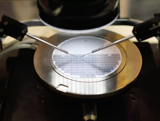
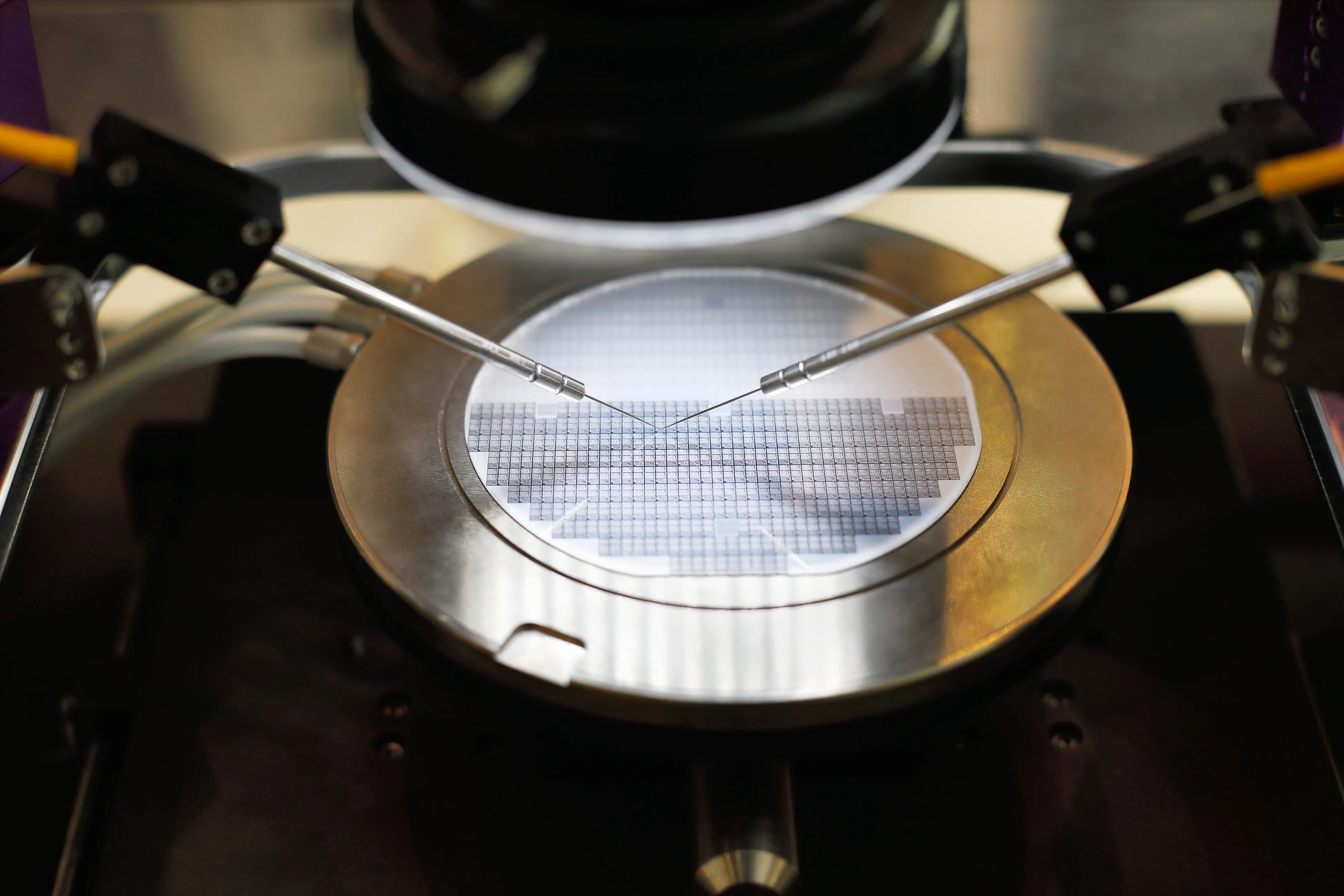
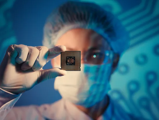
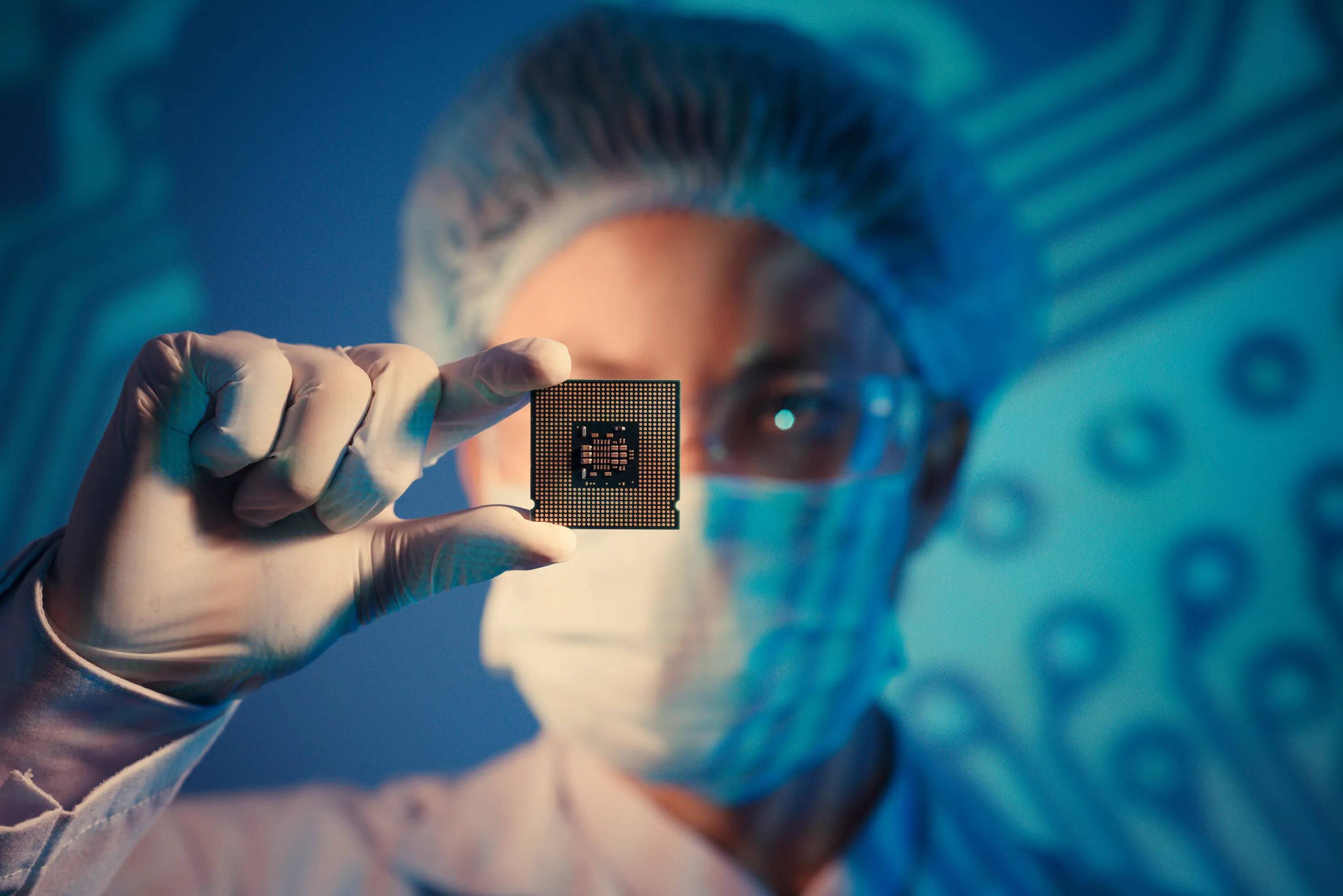
SEMI has long promoted the industry collaboration that has contributed to the rise of the smart digital world we live in today. A world where data is being generated continuously by systems, gadgets, and sensors around us – often referred to as the Internet of Things (IoT). In our personal lives, most of us have smartphones, smart watches, smart TVs and smart cars, and we live in smart homes and smart cities generating huge amounts of data.In the work world, data and analytics are now influencing almost every industry including healthcare, government, financial services, construction and transportation. This data has the potential to transform our lives and make our world even smarter – if we can communicate and process this data, and use it to come up with actionable recommendations or actions. Artificial Intelligence (AI) and Machine Learning (ML) techniques have generated much excitement precisely because they offer us ways to realize the full value of data by harnessing it and transforming it into active intelligence.Data-intensive technologies are required to store, communicate and analyze data. And it all starts with innovation in microelectronics chips and systems spanning processors, memory, sensors, radios and other devices, presenting a huge opportunity to producers of these technologies. However, with Moore's Law beginning to slow, technology paths and innovation options are diverging. Companies must swiftly assess these options in order to develop competitive offerings. But the technological complexity and divergence makes it increasingly expensive or even unaffordable for many companies to track and pursue these options.The good news is that cost-effective early assessment is possible through pre-competitive collaboration that can produce new and often unexpected cross-disciplinary insights by overcoming traditional silos in industry and academia. Unfortunately, important collaborative industry platforms, such as the International Technology Roadmap for Semiconductors (ITRS), have folded, opening a collaboration gap in the global microelectronics ecosystem.As part of its mission to help companies connect, collaborate, and innovate, SEMI has built a collaborative, cross-supply-chain platform – the Strategic Innovation Platform (SIP). The goal is to provide early and comprehensive assessment of future technologies that are five to eight years away from commercialization. The assessment identifies not just technical barriers but also manufacturing and supply-chain constraints to implementing new technologies. SIP brings together the entire microelectronics ecosystem including strategic technology thought leaders, subject matter experts, technology and application developers, academia, researchers, start-ups and government. With more than 2,100-member companies spread across the global electronics manufacturing supply chain, SEMI is uniquely positioned to enable this critical collaboration. Award-Winning First ProjectThe inaugural SIP project assessed key drivers of future technologies. A key finding was that fast, efficient interconnects between devices and components are critical to the system performance important to customers and users, implying that system-level optimization is required. For data-intensive applications, interconnects have emerged as a key bottleneck for both performance and power in various circuits and systems in part because the slowing of Moore’s Law has decelerated advances in individual device performance, and in part because systems are becoming more complex, requiring heterogeneous integration.To address this challenge, SIP brought together industry experts from ASE Inc., Dow Chemical, Lam Research, Qualcomm and Xilinx to assess the future impact of interconnects for data-intensive applications. SEMI also involved Stanford University professors to collaborate on modeling and simulation. Through this unique cross-disciplinary collaboration, SIP developed a realistic model to evaluate the system-level performance of single-chip systems, as well as multi-chip systems – including traditional 2D packages, high-performance 2.5D systems that use interposers, and futuristic 3D systems. SIP also explored supply chain challenges in business continuity, manufacturability, Environment, Health and Safety (EHS) and the regulatory environment. SEMI worked with a broad range of industry partners to ensure that the model parameters accurately reflected realities on the design and factory floors to ensure usable results. Experimentation has become ever more expensive, with one industry player reporting that “it costs us $100 million to do a good experimental evaluation.” Accurate models can go a long way toward reducing the cost of technology assessment. The SIP collaboration produced key quantifiable insights including comparisons that highlight the benefits and limitations of various materials being explored for future interconnects, and of architectures under consideration for future data-intensive applications. For example, the current workhorse for artificial intelligence (AI) platforms – 2.5D technology – delivers a 4X improvement over 2D packaging but falls short of providing the orders-of-magnitude improvement that future AI/ML applications may require. These findings enable the industry to begin to identify ways to optimize 2.5D architectures, transition to 3D heterogeneous integration for performance-critical applications in the medium term, and to eventually evaluate new paradigms such as neuromorphic and quantum. The project findings were presented late last year in the form of two research papers at Electronics System-Integration Technology Conferences (ESTC) and International Microelectronics Assembly and Packaging Society (IMAPS) recently. One received the “Best Paper of the Session” award at IMAPS – a recognition that affirms the power of a collaborative platform such as SIP to produce valuable insights to address the growing technology complexity within the microelectronics industry. The microelectronics industry is on the cusp of a historic inflection point, where it could fuel the rise of emerging applications in AI/ML and IoT, and can grow into a trillion dollar industry over the next several years. More importantly, the industry is poised to help solve some of society’s most complex problems in areas including healthy living, climate change and transportation. No company can do this alone, and pre-competitive platforms such as SIP are key both to accelerating innovation through cross-disciplinary collaboration, and to reducing costs for individual companies. Please contact Tom Salmon at [email protected] or Pushkar Apte at [email protected] for more details and to get involved in future projects.Tom Salmon is vice president of Collaborative Technology Platforms. Pushkar Apte is a strategic technology advisor at SEMI.
Read More
The more than 53,000 people who flocked to SEMICON Korea last month were treated to a motherlode of insight into the future of the semiconductor industry as 470 companies exhibited innovative technologies in more than 2,000 booths. But the annual event’s most arresting numbers came in keynotes and other presentations pointing to the extraordinary industry growth that lies ahead.“It is no exaggeration to say that 90 percent of the world’s data has been generated in the last few years,” said Jim Feldhan, president of Semico Research. “This explosive growth of data is expected to continue. That's why server shipments will grow by 20.3 percent, or 30 million units, this year alone.”Feldhan said that the Internet of Things (IoT) will be a chief driver of semiconductor industry growth, with IoT expected to be applied in areas as varied as automotive, smart cities, edge computers, finance, architecture, agriculture and healthcare. For its part, artificial intelligence (AI) will start to exercise human-like judgment. Feldhan noted that in many instances in these fields, “it is more accurate to apply AI and vision systems than to rely on traditional decision-making.”Yoon Jong Lee, senior vice president of DB HiTek, predicted that the Internet, AI and 5G will drive market growth. “Looking back over the past 30 years, semiconductor market growth was powered by PCs, the Internet and cell phones, yet last year memory accounted for 35 percent of total semiconductor sales, more than double the figure in 2016,” he said. He predicted that, in 2019, the foundry sector will outstrip the semiconductor market in growth, noting that the average growth rate of the semiconductor industry is expected to be 4.1 percent, compared to 7.1 percent for the foundry market. Clark Tseng, director of SEMI, reported that the strong semiconductor growth in 2018 is unlikely to continue in 2019 due to the decline in memory pricing, as well as mobile and PC demand. “Demand for semiconductors is likely to decline in the first half as the industry is still digesting inventory and rebound in the second,” Tseng said. Semiconductor industry growth headwinds include decreases in high-end smartphone purchases, PC demand and demand for DRAMs for servers in data centers, Tseng said. Declines in economic growth and consumption in China and the U.S.-China trade war will also contribute to a slowdown. However, Tseng noted that, over the long term, technology innovation will continue and that the semiconductor industry’s prospects remain bright.One key innovation will be the elimination of AI’s reliance on Internet connections in the future. In his opening day keynote, Eunsoo Shim, senior vice president at Samsung Electronics, emphasized that AI technology that operates without the Internet in the future is essential. “We are developing 'on-device AI' technology that incorporates AI algorithms in products such as smartphones and autonomous vehicles,” he said. "When on-device AI technology is implemented, it reduces reliance on the Internet, battery consumption, and data latency.” Reducing latency will significantly improve device response time.Walden C. Rhines, CEO Emeritus of Mentor, a Siemens business, predicted that AI will fuel rapid memory growth. The memory semiconductor (DRAM, NAND flash) market is expected to see a temporary slowdown this year, with the market expected to rebound in 2020. Rhines said that memory could be seen as an early market with rapid future growth, citing memory market super-booms in 1995 and 2000.“Memory production has not decreased since 1995 or 2000,” he said. “Although memory prices will temporarily fall this year after significant market growth in 2017 to 2018, the market will continue to grow as memory production increases,” he said. Rhines added that “although memory prices will drop by about 10 percent this year, he believes prices will increase 6 percent next year.” He also predicted the steady growth of the non-memory semiconductor market as AI technology matures and China’s investment in fabless companies continues.Indeed, SEMICON Korea speakers made it clear that concerns about the growth of the semiconductor industry are expected to be short-lived. While overall growth is likely to slow in 2019, the industry is expected to rebound steadily – powered by the semiconductor industry paradigm shift led by AI, IOT, and autonomous driving – and reach a new high of nearly $541 billion in 2020.Jaegwan Shim is a marketing specialist at SEMI Korea.
Read More