downloadGroupGroupnoun_press release_995423_000000 copyGroupnoun_Feed_96767_000000Group 19noun_pictures_1817522_000000Member company iconResource item iconStore item iconGroup 19Group 19noun_Photo_2085192_000000 Copynoun_presentation_2096081_000000Group 19Group Copy 7noun_webinar_692730_000000Path
Skip to main content
Default Banner Image

SEMI News

The U.S. on September 1 will levy a 10 percent tariff on $300 billion (List 4) worth of Chinese goods that until now were exempt from duties, President Trump said today. The trade action makes good on the U.S. president’s commitment to impose the new round tariffs in response to China’s failure to deliver on promises to buy more U.S. farm goods and to stop the flow of the painkiller fentanyl into the U.S. The 25 percent tariffs already in effect on $250 billion in goods will remain in place.The new list includes items used in the electronics industry but also encompasses retail products spanning the U.S. economy including clothing, toys and cell phones, exacting a more direct hit to U.S. consumers. A meeting between China and U.S. trade officials in Shanghai this week apparently did little to ease trade tensions. Both sides plan to meet again in September, though expectations for meaningful progress toward resolving their trade differences then are low.The U.S. believes China backtracked from commitments to changing its practices related to forced technology transfer and intellectual property theft. China denies making the pledges and insists on the removal of all tariffs as part of a settlement.The U.S. actions risk backlash from China including non-tariff barriers to trade such as licensing delays, more stringent business-related inspections, and an accelerated rollout of its unreliable entities list, China’s response to the U.S. decision to blacklist telecommunications giant Huawei. The list includes foreign companies, other organizations and individuals that China sees as national security threats or risks to China’s economy.SEMI will continue to urge both nations to reach an agreement consistent with its 10 Principles for the Global Semiconductor Supply Chain in Modern Trade Agreements. The principles encourage free and fair trade, open markets, and respect of IP among all players in the global electronics manufacturing supply chain.SEMI member companies impacted by the new U.S. tariffs or facing any new non-tariff barriers in China should contact Jay Chittooran, public policy manager in SEMI’s Global Advocacy Office, at [email protected] Russo is vice president of Global Industry Advocacy at SEMI.
Read More
On July 1st, Japan’s Ministry of Economy, Trade and Industry (METI) announced updated licensing policies and procedures on the export and transfer of controlled items and their relevant technologies to the Republic of Korea (ROK). METI’s stated purpose for the actions were “in order to ensure appropriate implementation of export control.”In particular, METI will tighten controls on certain items and their relevant technologies as follows: Remove the ROK from its “white list” of trusted partners, limiting the ROK’s preferential treatment for exports Mandate individual licenses for exports of certain chemicals including fluorinated polyimide, photoresist, and hydrogen fluoride – all used in semiconductor and electronics manufacturing – and technology transferred with exports of manufacturing equipment to the ROK. Bulk licenses for the chemicals will no longer be available. METI has indicated that its actions were not intended as punitive, but rather as necessary to ensure proper management of the export control system and the effective tracking of chemicals, materials and technologies that could be used to develop weapons of mass destruction (WMDs). Nevertheless, the trade actions are cause for concern as they could have a negative impact on our members operating in Korea and Japan and the global supply chain in general.After the METI announcement, SEMI immediately consulted its International Board of Directors and assembled a global advocacy response team comprised of SEMI member companies and SEMI regional presidents in both Japan and Korea to assess risks to SEMI members operating in both regions and to the industry’s global supply chain. Additionally, SEMI conveyed its concerns to Japan and ROK trade officials, stressing that the semiconductor industry will bear the brunt of the new measures if the trade dispute escalates.SEMI president and CEO Ajit Manocha said: “We informed both governments of potential impacts of an escalation to SEMI members, their economies and the global supply chain and are encouraging them to resolve their differences. SEMI’s focus is to ensure the global microelectronics supply chain remains strong and intact.”SEMI member companies have stated that METI and the Japan government have provided assurances that trade with the ROK will not be encumbered and that semiconductor companies will see minimal impact regarding export license approvals. To this end, SEMI will continue to engage our members in Korea and Japan, monitor the dispute as it continues to unfold, and facilitate regular meetings between industry and the involved governments to ensure that industry impacts are identified and risks are mitigated. In the event the dispute escalates, SEMI is prepared to take action in accordance with its Global Trade Principles.SEMI released its Global Trade Principles last year to provide guidance to governments around the world in developing policies that benefit both regional economies and the industry. These trade principles are based on SEMI’s four trade pillars of free and fair trade, open markets, supply chain growth, and respect for IP and national security.Member companies negatively impacted by any changes in Japan’s regulatory policies or with any questions should contact their regional SEMI office or Jay Chittooran, Public Policy Manager, SEMI Global Advocacy, at [email protected] Russo is Vice President of Global Industry Advocacy at SEMI.
Read More
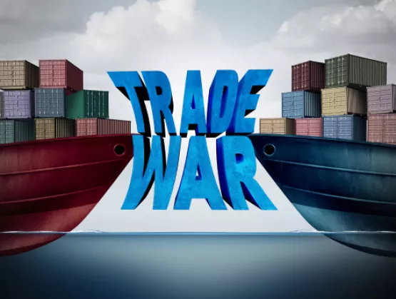
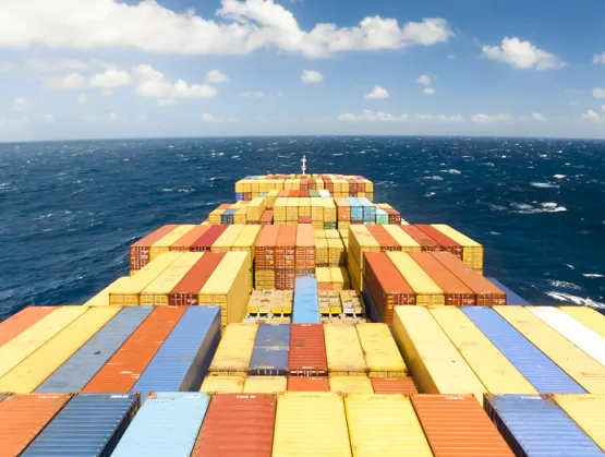
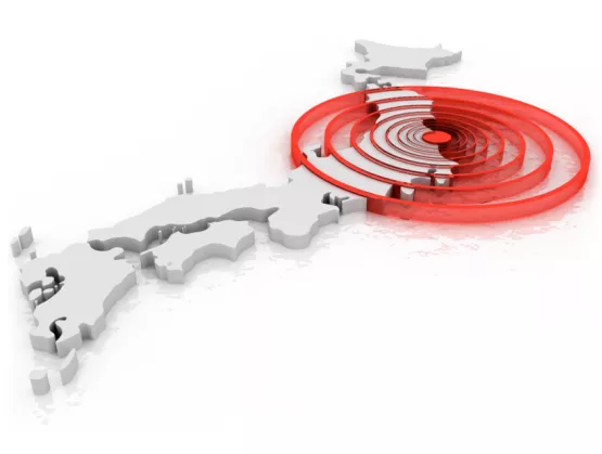
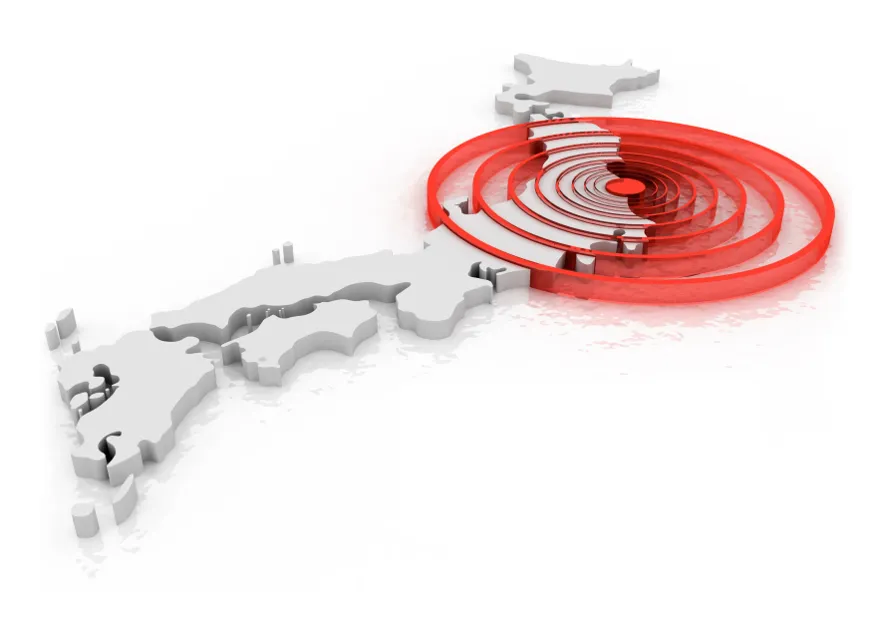
Wedged among four major tectonic plates, Japan is at the mercy of their abrupt herculean shifts and the earthquakes and tsunamis they can trigger. The fallout can be devastating. The magnitude 9 Great East Japan (Tohoku) temblor in 2011 and ensuing tsunami took nearly 20,000 lives, destroyed 138,000 buildings and cost $360 billion in economic damage.Factories including silicon wafer production facilities owned by Shin-Etsu Chemical and MEMC Electronic Materials – together accounting for 25 percent of the global silicon wafer production – sustained heavy damage. Operations were suspended. The Kumamoto earthquake in 2016 also caused significant damage. The economic cost: as much as $7.5 billion.With disaster risk rising on a global scale, these calamities offer valuable lessons in disaster preparedness and how companies can draw from their experiences to strengthen business continuity planning (BCP).Earthquake experiences and lessons in BCP were the focus of the recent SEMI Japan Members Day as speakers from five semiconductor device and equipment manufacturers offered their BCP strategies to about 150 SEMI members. Following are key takeaways from their presentations. Renesas: Create a robust production plant that is hard to break and easy to fixRenesas Semiconductor Manufacturing’s Naka plant took about 80 days to resume production while its ability to deliver semiconductors was delayed even longer as it recovered from damage caused by the Tohoku earthquake, said Yoshiyuki Miyamoto, Representative Director and President at Renesas. Operations at the company’s Kawajiri plant were disrupted by the Kumamoto earthquake.A key lesson from both earthquakes: The company needed to promote risk visualization from top-to-bottom in the supply chain. With the goal of making its plants easy to repair but hard to break down, Renesas implemented a risk management plan for earthquake preparedness plan to ensure stronger production line resistance and a stable supply to customers. The company ran simulations of multiple earthquake scenarios including aftershocks, enabling it to develop new BCP training and preparedness measures. Sony: Staying transparent about the disaster, sharing and interacting with related companiesYukihide Keigo, a representative from the Sony Semiconductor Manufacturing, showed footage taken the day the Kumamoto earthquake damaged a production line at its Kumamoto Technology Center. Sony is the top manufacturer of imaging sensors worldwide, and the Kumamoto plant is the backbone of that production. The magnitude of the foreshock fell within levels Sony had accounted for in its BCP at that time, and the line was expected to return to full production within a week. However, the magnitude of the earthquake that followed outstripped expectations, and the company’s BCP didn’t hold up. Three and a half months later, the plant had finally fully recovered. The protracted recovery prompted Sony to develop an earthquake preparedness plan using a model that assumed double the magnitude of expectations. For full restoration, the company identified challenges to returning to full operation at each stage of the production line. Then it went even further, developing in-house diagnostics, implementing critical path methods and strengthening earthquake resistance of equipment that manages bottlenecks for the restart of the plant. The revision of its BCP plan led to the establishment of a system to shorten the resumption of production after a major earthquake to just two months.Sony shared the contents of its BCP review with other companies to solicit help identifying any gaps and highlighted its partnership with Renesas in the Semiconductor Industry Association in Japan (JSIA), a committee of the Japan Electronics and Information Technology Industries Association (JEITA), to share materials procurement resources for the purposes of disaster preparedness and business continuity. HORIBA STEC: Steady daily practices protect hundreds of millions of yen worth of products HORIBA STEC’s Aso plant, near the epicenter of the Kumamoto earthquake, suffered heavy damage that cut off electricity and the water supply, yet production in its clean room resumed in just 10 days, said Hiroyuki Koyama, a factory manager at the plant. The plant’s quick recovery stemmed from daily preventive measures implemented before the quake such as connecting freestanding shelves for greater stability, applying thick rubber bands as rails to prevent manufactured goods from falling to the floor, and placing equipment on rolling carriages instead of fixed shelves.The practices saved the Aso plant hundreds of millions of yen in products and materials that otherwise could have been lost in the earthquake. Koyama also offered the reminder that, with regulations governing factory layout and construction differing widely depending on factors such as a building’s age, companies need to tailor their BCPs to the unique characteristics of each building. THK: The key point of dampening earthquakesTHK’s ACE Division develops earthquake dampening and vibration control devices designed to absorb the vibrational energy of an earthquake, though the devices must also be designed for precise analysis of that energy, said Hidemi Murao. Murao provided an overview of the latest technologies and products for dampening earthquake vibrations and shared test results from experimental devices.Murao described how THK’s recently introduced Linear Motion (LM) Guide, an earthquake vibration dampening technology, can significantly reduce building vibrations during a temblor. In a video Murao showed to demonstrate how the guide works, a shelf loaded with equipment rests on a platform equipped with THK’s LM Guide equipment. Simulating an earthquake, the platform shakes vigorously in every direction but the shelf remains steady as the LM Guide dampens the vibrations. The platforms can be installed on floors or underground in buildings or factories to prevent shelves from toppling. Tokyo Electron: The ideal BCP management systemOne risk associated with BCP training is that it can become overly routine, dulling the response of employees in actual disasters, said Tokyo Electron Vice President Tatsuya Aso. To help keep its workers’ skills sharp, TEL held surprise drills with employees assigned to particular BCP roles to test their ability to adapt quickly to when disaster strikes. In addition, TEL has launched surveys in more than 70 overseas locations to optimize safety in these high-hazard facilities.The SEMI Japan Members Day presentations made clear that the issue of BCP transcends boundaries between individuals, manufacturers, regions, and sectors within the global electronics supply chain. Disaster preparedness requires problem-solving across the entire supply chain, with companies sharing technical knowledge, offering mutual aid, and striving for continual improvement. Collaborative is essential. At SEMICON Japan 2019, SEMI will continue to bring companies together to address BCP initiatives and share their technical knowledge with members. Jim Hamajima is president of SEMI Japan.
Read More
In testimony today before a U.S. government interagency panel considering tariffs on $300 billion worth of Chinese goods, SEMI called for the removal of about 30 tariff lines, which cover items central to the semiconductor manufacturing process.Mike Russo, vice president of global industry advocacy at SEMI, explained in his testimony that while SEMI strongly supports efforts to better protect valuable intellectual property (IP), tariffs will not help address Chinese trade practices, and will ultimately have significant and unintended consequences.SEMI asserts that these tariffs will harm not only companies operating in the U.S., but other companies as well in the semiconductor supply chain by increasing costs, introducing uncertainty, and most problematically, stifling innovation. Collectively, SEMI estimates that this round of tariffs will cost its 430 U.S. members millions annually in additional duties. All told, SEMI estimates that all U.S. and Chinese retaliatory tariffs will cost members nearly $800 million in annual duties.SEMI’s full written comments note that these tariffs, on top of those already in force and the retaliatory tariffs, will hamstring the industry. The tariffs seem to target firms for simply operating in China. Given that tools, materials, and related products are extremely complex, precise, and difficult to manufacture, it is unreasonable to believe that a constituent component can simply be replaced with a part or tool from another source. Further, this U.S. government approach does not take into account that many items subject to these tariffs are not available, at sufficient quality and cost, from domestic sources, or even non-Chinese sources.Over the past year, SEMI has submitted written comments and offered testimony on the three previous rounds of tariffs, which covered about $250 billion worth of Chinese goods, or about half of all imports from China. The tariffs hit various components in the electronics manufacturing supply chain critical to the semiconductor industry, including materials and equipment used to manufacture wafers, boules, and chips as well as test, inspection and sensing equipment. We urge SEMI members to review the $300 billion U.S. tariff list to determine the level, if any, of impact. We also strongly encourage members to review Chinese retaliatory lists as well. Any SEMI members with questions should contact Jay Chittooran, Global Public Policy Manager at SEMI, at [email protected].
Read More
The world of work is transforming. I believe digitalization can be a force for better quality work, unleashing higher productivity and opening up new opportunities to work in different ways. For this to happen, we must set the right framework. We must set the right conditions to enable everyone to reap the benefits from the digital era.One crucial condition is that people have the right skills. That's why the European Commission launched a "Skills Agenda for Europe" in 2016. It sets out 10 actions to make the most of Europe’s human capital, which is crucial to keep Europe on a competitive edge and growing. One of its focus areas for example is better skills intelligence – understanding skills bottlenecks and anticipating needs, including through stronger business-education partnerships. Education needs to be more responsive to labour market needs.The microelectronics industry is one such area in Europe that faces an acute talent shortage. But this technology is crucial for Europe’s competitiveness. Microelectronics enable many of the key technologies and innovations required for advancing a secure, sustainable and digital economy. Data centers, online platforms, autonomous spacecrafts, blockchain algorithms and 5G infrastructure may serve different purposes but share one vital element: microelectronics. The deepening penetration of electronics in the digital economy and new applications is giving rise to industry requirements for a workforce pool with soft skills and expertise in production technologies, software and data science.This is why the European Commission encourages new collaboration models between the worlds of education and industry across all business sectors, including in microelectronics. I welcome the fact that SEMI, the industry association representing the electronics manufacturing supply chain, is fully committed to building and maintaining the needed talent pipeline in Europe. I wish you best of luck in your endeavors. Marianne Thyssen is European Commissioner for Employment, Social Affairs, Skills and Labour Mobility.
Read More
SEMI, with 660 other companies and associations, urged the Trump Administration in a letter today not to escalate its trade dispute with China by imposing new tariffs and to negotiate a resolution. The letter comes as the Office of the United States Trade Representative prepares for hearings next week in considering 25 percent tariffs on $300 billion worth of Chinese goods, including a number of products used in semiconductor manufacturing.With intellectual property (IP) the crown jewel of the semiconductor industry, SEMI vigorously supports the stronger IP protections direly needed in international trade. However, we worry that the proposed and recently implemented tariffs will hurt companies in the semiconductor supply chain by introducing significant uncertainty, increasing costs and subjecting companies to retaliatory tariffs while ultimately doing nothing to address our concerns regarding China’s trade practices. We strongly encourage the administration to return to the negotiating table while working with our allies to develop global, enforceable trade solutions. There are no winners in a trade war. Senior industry executives and SEMI staff raised this and other issues with policymakers last month as part of SEMI’s Spring Washington Forum. SEMI will continue to engage the Trump Administration as trade tensions continue.Jay Chittooran is public policy manager at SEMI. He can by reached at [email protected].
Read More
Tensions between the United States and China have reached fever pitch. Ongoing trade negotiations between the U.S. and China broke down earlier this month over reported backpedaling by China on key concessions in a proposed Trump administration deal. Over the past year, the U.S. has raised tariffs on more than $250 billion worth of Chinese goods to 25 percent, and last week the administration proposed tariff hikes on an additional $300 billion in imports – moves that have drawn retaliatory tariffs from China, many squarely hitting the semiconductor industry. Based on SEMI member feedback, the tariff increases will cost the semiconductor industry more than $750 million annually.At the same time, the Trump Administration is taking other steps to ratchet up pressure on China. Last week, seven months after placing Fujian Jinhua on the Entity List, which effectively blocks the sale of and export of goods to China, the U.S. Department of Commerce added Huawei (and nearly 70 affiliates) to the list. While the U.S. is taking this action for security reasons, it is also seen as a move to create leverage at the trade table. The U.S. is also intensifying efforts to reform the export control regime, focusing first on enhancing controls on emerging technologies and then on foundational technologies. The rising pressure has prompted China to contemplate and launch a counteroffensive that goes well beyond tariffs and export controls. The reprisals include China’s promotion of heightened Chinese nationalism by domestic consumers, a tactical slowdown of administrative processes required to conduct business in China, and the imposition of direct or indirect limits to market access. China is also using U.S. actions to justify larger state investments in its domestic industry and is ramping up efforts to give other regions greater access to its markets as it works to strengthen those relations ahead of next month’s G-20 summit in Osaka, Japan. The U.S. is also maneuvering to bolster its negotiating hand through its own agreements with Japan and the European Union.Unintended consequences of Trump administration actionsThe Trump administration’s moves to rectify the trade imbalance with China are also well-intentioned in seeking to protect the IP of U.S. technology companies and ensure continued U.S. leadership in technology development and innovation. However, its tactics can encourage long-term, perverse shifts in the globally integrated electronics manufacturing supply chain that risk upending market-driven investments in the semiconductor industry and weakening natural market forces that nourish competition among companies based on service, quality and product offerings.It is critical for SEMI, in working with government officials, to shed light on the potentially deep, unintended damage its trade actions can wreak on global supply chains and markets. We will continue to promote global standards governing trade, IP and market access through our Global Trade Principles and focus on sustaining a global order that assures the electronics manufacturing supply chain remains cohesive and vibrant.SEMI continues efforts to influence trade policyWe continue to meet with government policymakers around the world to educate them on near- and long-term impacts and risks of their evolving trade practices, conducting approximately 220 meetings with government officials globally in the past year. We also facilitate individual and group member meetings to give SEMI members direct contact to key government decision-makers. For example, on May 22nd during the SEMI Spring Washington Forum, or “fly-in,” more than 30 semiconductor industry executives from across the supply chain met with administration officials and Congressional offices to discuss issues including trade, export controls and immigration reform and impacts on their businesses. The executives represented a cross-section of small, medium, large and global companies based in the U.S. or providing support for U.S. organizations. Their aim: influence policy development. SEMI is in a unique position as a representative of the end-to-end, global electronics manufacturing supply chain and is a valuable “one-stop-shop” that represents members on policy while providing opportunities to collaborate in one of our Technology Communities. SEMI members can also leverage our strategic partnerships, our market research or leadership in industry standards. With this breadth and depth of member engagement and industry expertise, SEMI leads in providing industry insights to governments at this critical time. There is no doubt that the current situation is complicated and it is impossible to predict when or how the trade issues will be settled. As the U.S. and China work to settle the trade dispute, SEMI will continue to lead efforts to ensure that the voices of SEMI members and the electronics industry supply chain are heard.Mike Russo is vice president of Global Industry Advocacy at SEMI.
Read More
On behalf of its global membership, SEMI is actively addressing a variety of environment, health and safety (EHS) dossiers impacting the semiconductor manufacturing supply chain. Together with its dedicated working groups (WGs), SEMI educates regulators globally on semiconductor manufacturing technology and advocates a balanced policy framework supporting innovation, growth and sustainability.Perfluorooctanoic acid and related compounds and salts (collectively known as PFOA) have been on the radar of the SEMI PFOA WG and EHS Advocacy Program for several years. PFOA is reported to cause severe and irreversible adverse effects to the environment and human health. PFOA is very stable and will last for years in the environment, and so it is considered a Persistent Organic Pollutant (POP). As such, PFOA is in scope of the Stockholm Convention and meetings to consider revisions to the Convention take place regularly. During these consultative meetings, Parties to the Convention are invited to provide observations and propose amendments. SEMI participated in the ninth meeting of the Conference of Parties (COP) in Geneva in late April and early May to provide the position of the semiconductor manufacturing industry.Among the many substances used to manufacture equipment components, fluoropolymers and fluoroelastomers (together known as fluoromaterials) have been produced sometimes with PFOA as a processing aid. To reduce hazardous effects to the environment and human health and to meet regulatory obligations, many (but not all) fluoromaterial manufacturers worldwide have been eliminating PFOA from their processes. Over the past several years, the WG has been studying equipment components – as well as related supply chains – that might contain fluoromaterials made with PFOA. The WG has learned that if PFOA is present in fluoromaterials, it is only as an unintentional contaminant or impurity. The WG has also confirmed that PFOA serves no intended purpose or performance function in the fluoromaterial-containing components that might be present in semiconductor manufacturing equipment. Although more testing is needed, the WG also believes PFOA that might be present in fluoromaterials does not move freely out of the material into the surrounding environment. In this light, the WG reviewed a draft of exemption recommendations from the Persistent Organic Pollutants Review Committee (POPRC) to the full Stockholm Convention. The exemptions in the draft recommendations addressed new and legacy equipment, fabrication plant-related infrastructure and related refurbishment parts for the manufacture of semiconductors and related electronic devices, and it imposed a commitment to remove any ‘PFOA residue’ from equipment components in five years (10 years for legacy equipment and refurbishment parts). Additionally, there was also an exemption in the draft for PFOA related to photo-lithography and etch processes, which the WG fully supported to maintain, as the presence of PFOA in process chemicals is fairly well understood, but viable substitutes have not yet been found for some applications.The outcome of the WG review was a concern because the equipment-focused exemptions introduced the concept of a ‘PFOA residue,’ and the Stockholm Convention already contains an exemption for ‘Unintentional Trace Contaminants’ (UTCs). The WG concluded that the existing UTC exemption was already sufficient. Additionally, although the WG does have spot information that PFAO can be present in fluoromaterial components, there is no comprehensive data about PFOA presence throughout the deep and complex equipment component supply chain, particularly regarding older parts in storage.Additionally, the WG has seen that very low levels of PFOA can be unintentionally created by some fluoromaterial post-processing steps such as processes intended to control PTFE polymer chain length in fluoro-lubricants that unintentionally create small quantities PFOA (note that PFOA is roughly a very short PTFE chain with a ‘carboxyl’ ending). Also, the WG has learned that PFOA can, in some cases, be accidentally created from fluoropolymers, adding to doubts as to whether ‘PFOA free’ can be determined or achieved. Therefore, the commitment contained in the draft exemption to have all ‘PFOA residues’ removed in five or 10 years was not based on a well-defined action timeline.Therefore, the WG in its discussions with governments around the world, prior to and during the Stockholm Convention COP meetings, requested the removal of specific exemptions related to equipment used in semiconductor manufacturing. The WG also requested that the specific exemption related to photolithography or etch processes be maintained. SEMI appreciates that its recommendations were accepted by the COP. This will help avoid country-specific regulations based on the Convention that are not fit-for-purpose. SEMI and its WG will continue to study PFOA and its elimination from the semiconductor manufacturing supply chain, and educate regulators globally on semiconductor manufacturing technology, underpinning sustainability, innovation and growth in a balanced manner.
Read More
On May 8, a group of students gathered at SEMICON Southeast Asia for a one-of-a-kind experience. These students would be the first in the region to participate in SEMI High Tech U (HTU) – diving into the deep technology at the core of our industry. They simulated the layering process used in the wafer fabs for microelectronics and solar cell fabrication, then identified uses of integrated circuits and how the process evolves from materials (silicon) to product (patterned wafers).Nearby, another group of students jumped into lessons about gates and binary logic, the language of computers and how they communicate. They played with four basic logic gates – “AND”, “OR”, “NOT” and “XOR” – by using logic boards. Then it was high time to apply what they learned about gates and the binary systems – the inner workings of a calculator – and launch into the much-anticipated Human Calculator game. During the game, students become a 2-bit adder. First, they must convert numbers into binary and then trace the digits through a series of gates. It's only with careful communication and concentration that teams get the right outputs.HTU is the SEMI program that introduces students to science, engineering, technology, and math (STEM) through hands-on activities and experiential learning led by industry volunteers. Since 2002, HTU has reached some 8,000 students in 12 states and nine countries.Southeast Asia hosts first HTUThe ‘Human Calculators’ were one of two groups of more than 80 high-school students from four schools who came to the Malaysia International Trade and Exhibition Centre (MITEC) in Kuala Lumpur for a fun day of education and workshops. The sessions were led by instructors Shafiq Shahmeen and Zafryl-Zaheidy Mustofa from Inari-Amertron and Jamaludin Johar and Huichin Chew from STMicroelectronics.Kicking off the sessions, High Tech U program manager Bryson Gauff gave an oral history of HTU with the students and their teachers and prepped them for the exciting workshops.From India to the United States – Ajit Manocha’s inspiring storySEMI president and CEO Ajit Manocha, on stage for the ribbon-cutting to celebrate the Southeast Asia’s first HTU, shared the story of how he was moved to enter high technology at a young age. Growing up in New Delhi, India, Ajit developed his passion for engineering after being inspired by a close family friend. His love of bits and bytes led him to the United States, where he started his career at Bell Labs, working with semiconductors. Reflecting on his past, he told the students that if a young boy from New Delhi can become an engineer and move to the U.S. to pursue his dream, everyone in the room can do it too – whatever their passion. Much like his friend as a youth, Ajit paid it forward by encouraging the students to follow their hearts: “The future is yours and you can be whatever you want to be.” Ajit Manocha and Professor Madya were joined onstage by Kai Fai Ng, president of SEMI Southeast Asia, and Leslie Tugman, SEMI VP of Global Workforce Development and Diversity, for the ribbon-cutting at SEMI High Tech U in Southeast Asia. The power of experiential learning YBrs. Prof. Madya Dr. Wan Zuhainis Binti Saad, Director of Academic Development Management, Ministry of Education, lit up the room with her passion for education. She quickly connected with the students as she shared her story of being a microbiologist and a professor. She encouraged the students to learn together and do what they love. A strong advocate for empowering learners, Professor Madya also offered a transformational approach to teaching students in the 21st century education – a dynamic, forward-thinking mix of passion-based learning, experiential learning, and entrepreneurial innovation.She believes the more students blend STEM studies with other curriculum like the arts and humanities, the better they can work collaboratively and develop their passion in life. Professor Madya thrilled the roomful of students with her message about what the future holds for all students, especially those participating in Southeast Asia’s first-ever High Tech U.The future of electronicsWith today’s semiconductors processing data at blurring speeds, the program ended aptly with awards for quickness. The awards ceremony, sponsored by Edwards Technology Singapore, recognized the winning team for the fastest Human Calculator in each session. And all four schools received certificates for participating in High Tech U to celebrate the work of all the students – the faces of the future of electronics.SEMI welcomes Southeast Asia to the global High Tech U community! To learn more about SEMI HTU please visit our website. The first-ever SEMI HTU Southeast Asia students with their teachers, industry volunteers and HTU staff at SEMICON Southeast Asia. Ariana Raftopoulos is a marketing communications manager at SEMI.
Read More