downloadGroupGroupnoun_press release_995423_000000 copyGroupnoun_Feed_96767_000000Group 19noun_pictures_1817522_000000Member company iconResource item iconStore item iconGroup 19Group 19noun_Photo_2085192_000000 Copynoun_presentation_2096081_000000Group 19Group Copy 7noun_webinar_692730_000000Path
Skip to main content
Default Banner Image

SEMI News

Last week, more than a dozen senior semiconductor executives traveled to Washington, DC for the first-ever Fall Washington Forum. The SEMI Washington Forum, a venue for SEMI members to educate lawmakers about the industry, focused on action against China, both in the form of tariffs and export controls.Our industry is global, and companies rely heavily on trade. In 2017, more than 90 percent of equipment made in the United States was exported. Because of this dynamic, the United States holds a nearly $9 billion trade surplus in this industry. SEMI supports trade policies that open foreign markets. In the meetings, the executives expressed deep concern that the tariffs would inflict deep damage to the U.S. economy, including to SEMI members. Estimates suggest that the Sec. 301 tariffs (and the Chinese retaliatory tariffs) will cost semiconductor companies more than $700 million annually, dramatically increasing the cost of doing business. These tariffs also threaten U.S. technological leadership. The United States has led innovation for decades. However, by pursuing policies that limit market access opportunities, company-led R D and innovation will slow, which, in turn, will curb further export potential. SEMI companies also stressed that because of the blunt application of these tariffs, this action will actually hurt U.S. companies as much as it hurts their Chinese competitors. Indeed, about 40 percent of imports in our sector from China are from U.S. or other non-Chinese companies. Further, the semiconductor industry relies on a vast network of supply chains, which have been built and qualified over the course of years. A fundamental revamp of supply chains is simply not feasible. This would be expensive, time-consuming, and resource-intensive. With a growing number of policy issues that are central to and could have significant impact for semiconductor companies, SEMI hosted its first ever Fall Washington Forum for members of its North American Advisory Board (NAAB). SEMI also invited several other industry executives. In total, 14 senior industry executives, including representatives from equipment manufacturers, component suppliers, and materials providers, attended the Fall ForumDuring the two days of meetings, SEMI met with several senior Administration officials to better the policies being enacted and considered as well as encourage all parties to not impose barriers to commerce, which would severely impact the semiconductor industry. SEMI also met with Members of Congress and their staffs on this issue. All told, attendees at the Fall Forum had more than 15 meetings with policymakers, reflecting the great impact of public policy on SEMI members companies. At a time when the stakes for the industry could not be higher, direct engagement with lawmakers is critical. The Washington Forum offers an incredible opportunity for members to better understand the impact of key public policy issues and gain firsthand experience in influencing policy and helping lawmakers better understand the industry.If you are interested in learning more about the SEMI Washington Forum or SEMI’s public policy program, please contact Jay Chittooran by email at [email protected].
Read More
Over the past three decades, most of the world’s innovations have centered largely on business models and involved iterative advances of existing technologies, with none matching the global impact of the top 10 semiconductor industry discoveries and advances, Dr. Morris Chang, founder of TSMC and the IC foundry model, said at SEMICON Taiwan 2018 this week.Few have as clear a perspective on the transformative power of semiconductors as Dr. Chang, founder of TSMC and father of the IC foundry model. Keynoting the IC60 Master Forum celebrating the 60th anniversary of the invention of the integrated circuit (IC), Dr. Chang listed what he considers the 10 key semiconductor industry innovation milestones since 1948:1. Invention of the transistor by Shockley, Bardeen, and Brattain – 19482. Silicon transistor – 19543. Integrated circuit – 19584. Moore’s Law – 19655. MOS technology MOS FET – 1964 Silicon gate – 1967 CMOS – 1970 6. Memory DRAM – 1966 Flash – 1967 7. Outsourced assembly and test (OSAT) – 1960s8. Microprocessor – 19709. VLSI systems design – 1970-1980 IP and design tools – 1980-present 10. Foundry model – 1985 Among the most consequential semiconductor advances may be yet to come, Dr. Chang said, citing innovations including artificial intelligence (AI) and machine learning, new device architectures, Extreme Ultraviolet lithography (EUV), 2.5D/3D packaging, and new materials such as graphene and carbon nanotubes.Dr. Chang argued that because bringing an innovation into production is immensely more expensive than proving a theory in a lab, innovators are not always the ones to implement and benefit from their novel ideas. Today, innovation costs are skyrocketing, driving more consolidation across the supply chain.Michael Droeger is director of marketing at SEMI.
Read More
The arrival of Fan-Out Panel Level Packaging (FO-PLP) appears to be at a perfect time: This technology will leverage processes developed for Three Dimensional Stacked Integrated Circuits (3DS-IC) as well as panel processing technologies developed for industries such as solar panels and large-screen TVs. In this combination, FO-PLP promised the improved performance of 3DS-IC, without the expense. There was just one problem…That problem is the size of the panels to be processed. As different companies developed FO-PLP processes, they chose panels sized to meet certain technical or business goals, or chose a size based on familiarity. So, processes were being developed for more than ten sizes, each of which had one or more companies championing them. For people in the wider semiconductor industry, the development of many processes, each with a unique panel size brought a feeling of déjà vu, reminding them of the 1970s, when each device manufacturer created their own specification for wafer size, forcing them to manufacture their own wafer processing equipment since no external manufacturer was willing to produce tools usable only by a single customer.SEMI responded by developing an industry consensus silicon wafer standard – which described basic parameters, including diameter and thickness – to resolve the issue. Almost overnight the landscape changed, and new tool manufacturers sprung up, enabling the incredible growth that has persisted over more than 40 years.Recently, Cristina Chu (TEL NEXX) presented the state of FO-PLP to the North America Chapter of the SEMI Three-Dimensional Packaging and Integration (3DP I) Technical Committee, suggesting that the Committee develop a single standard dimension that would enable the technology to move into high-volume manufacturing.The Committee began by surveying the industry to determine the interest level in such a standard as well as its contents. A key finding came in response to the question “Would you support a standardized panel size?” Overwhelmingly, over 70 percent of the respondents supporting the idea for the standard, with less than 2 percent opposed. The survey also asked if other parameters should be standardized and, if so, which parameters. Majority responses pointed to edge profile, flatness, and warp, prompting the 3DP I Committee to immediately form the FO-PLP Panel Task Force (TF) to develop such a standard. Chu and Richard Allen (NIST) agreed to chair the TF and respondents to the survey were asked to participate as TF members.The TF initially decided to follow the model of SEMI M1, Specification for Polished Single Crystal Silicon Wafers, and write the document as a purchase specification. The purchase specification would indicate a limited number of mandatory parameters, identified as those that serve as bottlenecks to the development of a FO-PLP ecosystem. Parameters that were not perceived as bottlenecks but might be useful for implementing a FO-PLP process would be included as optional.Working under the SEMI Standards umbrella allowed the TF to take advantage of work done in the development of other standards, without having to recreate it from scratch. In particular, Flatness and Shape were repurposed from SEMI M1, ensuring consistent definitions of these parameters.The TF could not come to consensus on how the other parameters should be categorized, so the decision was made to move the ordering table to a new Appendix as optional.The TF will be balloting its first specification for panel substrate in the upcoming cycle, which opens September 5, 2018 (Cycle 7). The voting is open to all industry experts. Based on the feedback, the task force will continue to refine and otherwise improve the specification by incorporating other parameters that are critical to making FO-PLP a reality.SEMI Standards development activities take place throughout the year in all major manufacturing regions. To get involved, join the SEMI International Standards Program at: www.semi.org/standardsmembership.For more information regarding FO-PLP Panel Task Force activities, please contact Laura Nguyen at [email protected] Allen is a physicist in the Nanoscale Metrology Group in the Engineering Physics Division of the Physical Measurement Laboratory (PML) at the National Institute of Standards and Technology (NIST).
Read More
In testimony today before a U.S. government interagency panel considering tariffs on $200 billion worth of Chinese goods, SEMI called for the removal of nearly 100 tariff lines, all of which cover items critical to the semiconductor manufacturing process, including materials and machines.Jonathan Davis, global vice president of advocacy at SEMI, explained in his testimony that while SEMI strongly supports efforts to better protect valuable intellectual property (IP), tariffs will not help address Chinese trade practices, and will ultimately have significant and unintended consequences. SEMI asserts that these tariffs will harm companies in the semiconductor supply chain by increasing business costs, introducing uncertainty, and stifling innovation. Collectively, SEMI estimates that this round of tariffs will cost its 400 U.S. members more than tens of millions annually in additional duties. All told, SEMI estimates that all U.S. and Chinese retaliatory tariffs will cost members nearly $700 million in annual duties. SEMI’s full written comments note that these tariffs, on top of those already in force and the retaliatory tariffs, will hamstring the industry. The tariffs seem to target U.S. firms for simply operating in China. Given that tools and materials are extremely complex, precise, and difficult to manufacture, it is unreasonable to believe that a constituent component can simply be replaced with a part from another source. Further, this U.S. government approach does not take into account that many items subject to these tariffs are not available, at sufficient quality and cost, from domestic sources, or even non-Chinese sources. We stand steadfast in our belief that this trade action will raise prices, put thousands of high-paying and high skill jobs at risk, and curb growth.Over the past four months, SEMI submitted written comments and offered testimony on the two previous rounds of tariffs, citing the damaging impact tariffs would have on the U.S. semiconductor industry. The first round of tariffs – on $34 billion worth of Chinese goods – took effect July 6, and the second round – targeting $16 billion in Chinese imports – will be imposed on August 23. The tariffs hit machines and tools central to the semiconductor industry, including equipment used to manufacture wafers, boules, and chips as well as test, inspection and sensing equipment. We urge SEMI members to review the $200 billion U.S. tariff list to determine the level, if any, of impact. We also strongly encourage members to review Chinese retaliatory lists as well. Any SEMI members with questions should contact Jay Chittooran, Public Policy Manager at SEMI, at [email protected].
Read More
SEMI has launched a mentoring program that pairs seasoned industry professionals with university students and professionals wanting to advance their careers. The program is designed to help tackle the semiconductor industry’s workforce shortfall and prepare the next generation of innovators. Under the program, SEMI members with years of professional experience share their knowledge with developing talent and help build their professional networks as they embark on their careers in the microelectronics industry.As the microelectronics manufacturing industry faces increasing challenges in recruiting, training and retaining a diverse pool of highly skilled talent to sustain the remarkable pace of innovation globally, SEMI has made workforce development a top strategic priority. Globally, the industry is confronted with more than 10,000 job vacancies.To help build the workforce of the future, SEMI has rolled out industry-wide programs to address a chief reason for the workforce shortage – increasing competition from other technology sectors. The initiatives include enhancing industry awareness of the industry’s critical need for talent, increasing the representation of women, and supporting young professionals and university students soon to be making important career decisions. The new SEMI Mentoring Program builds on those initiatives by guiding the next generation of innovators.With mentoring a proven method to develop talent, SEMI has contracted with Chronus – an experienced provider of a software mentoring platform tailored to support the SEMI Mentoring Program.SEMI Mentoring Program: Roles and Responsibilities This is a formal relationship in which mentors guide mentees in their professional development. The mentor will answer questions and take a personal interest in, guide, encourage, and support the mentee. The mentor will meeting monthly with the mentee and follow up as needed. The mentee will set up the first meeting to discuss professional goals, topics he or she would like to cover and timing for subsequent. Both mentor and mentee will commit to remain connected for at least six months. Frequently Asked Questions Q: How are meetings conducted?A: Mentors and mentees can meet face-to-face or virtually, but should meet for a minimum of one hour once a month for six months.Q: How are goals set?A: The mentor and the mentee agree on goals during their first meeting. The mentee is responsible for arranging meetings, preparing the agendas, and any other pre-meeting work. This will ensure that the discussions touch on the topics that matter most to the mentees.Q: What happens once the six months are up?A: You can continue an unofficial relationship if both parties agree, or you can search for a new mentor or mentee by reapplying through your mentor profile.Q: What is SEMI’s role?A: SEMI is here to help match you based off your preferences, facilitate the relationship, provide materials to guide your experience, and help resolve any program or platform related issues.Q: What are the program eligibility requirements for mentors?A: A mentor must be an employee of a SEMI member organization with a minimum of five years’ professional experience to mentor a university student, or seven years’ professional experience to mentor a developing professional.Q: What are program eligibility requirements for mentees?A: Developing Professional Program Developing professional, 0-7 years in their career Employed by a SEMI member organization University Program At minimum, a rising junior enrolled in a university program (students through PhD level accepted) Completing a STEM major Within 6 months of graduation if currently out of school and seeking employment Preferred: Interest in the microelectronics industry Q: Why be a mentee?A: Learn from an experienced industry professional and accelerate your professional development.Q: Why be a mentor?A: Being a mentor will allow you to grow as a leader while giving you the rewarding experience of guiding someone’s growth path firsthand. Join us in shaping the future of our industry by becoming a mentor or mentee. Sign up here! For more information about the program, please contact Cristina Sandoval, manager of Workforce Development, at [email protected].
Read More
U.S.-China Trade War Heats UpThe U.S. Trade Representative (USTR) yesterday released a 25 percent tariff on $16 billion in imports from China, including 29 tariff lines that represent the heart of the semiconductor industry. These tariff lines include semiconductor products such as machines and spare parts used to make, wafers, flat panel displays, masks and chips, and will cost SEMI’s 400 U.S. members an estimated more than $500 million annually in additional duties.SEMI, along with hundreds of companies, including Lam Research and KLA-Tencor, submitted written comments, requesting the removal of tariff lines from the proposed list. SEMI also testified on behalf of the semiconductor industry, joining more than 80 other companies, including Applied Materials, in opposing the duties before an U.S. government interagency panel in late July.This trade action is on top of the already imposed $34 billion U.S. tariff list, which will cost SEMI’s U.S. members tens of millions of dollars annually. In the coming days, USTR will publish details on how U.S. companies can request the exclusion of products from the $16 billion tariff list, much as it did for the first round of $34 billion.In a swift retaliation, China announced a 25 percent tariff on $16 billion in U.S. exports, including products vital to semiconductor manufacturing such as chemicals, test equipment and other parts. Both U.S. and China tariffs will take effect on August 23.The new tariffs come as China considers tariffs on $60 billion of U.S. imports, and the U.S. weighs additional duties on $200 billion of Chinese imports – a wave that would inflict even deeper damage on the U.S. semiconductor industry. This latest round of U.S. tariffs would cover goods used in microelectronics manufacturing, including chemicals, glass products and spare parts. SEMI will testify against the $200 billion tariff list later this month. If your company expects to be impacted by the proposed tariffs on $200 billion worth of goods, please contact SEMI staff.SEMI stands firm in its belief that none of the tariffs address U.S. concerns over China’s trade practices. Instead, they harm companies in the semiconductor supply chain by increasing business costs, introducing uncertainty and stifling innovation. SEMI will continue to engage with policymakers as both the U.S. and China $16 billion tariff lists are implemented. We will also be evaluating the products covered by the $200 billion U.S. list and the $60 billion Chinese list as both are further considered. We encourage members to review these lists to determine impact on their companies. For more information, please contact Jay Chittooran, Public Policy Manager at SEMI, at [email protected].
Read More
Did you miss the SEMI International Standards Reception at SEMICON West 2018? Not to worry, here are the highlights.SEMI honored two Standards industry leaders for their outstanding accomplishments in developing Standards for the electronics and related industries.Two awards were given recognizing the efforts of each member. The Technical Editor Award recognizes the efforts of a member to ensure the technical excellence of a committee’s Standards. This year’s recipient is Sean Larsen of Lam Research. Mr. Larsen has led the North America EHS Committee and multiple EHS task forces for over a decade. His knowledge of the Regulations, Procedure Manual, and Style Manual, combined with his vast experience in the industry, ensures that complex safety matters are explained in a clear, consistent manner, and ballot authors frequently rely on him for his technical skills in preparing ballots.In addition to co-chairing the North America EHS Committee, Mr. Larsen is currently the co-leader of the SEMI S22 (Electrical Design) Revision TF, the SEMI S2 Non-Ionizing Radiation TF, the SEMI S2 Korean High Pressure Gas Safety TF, and the Control of Hazardous Energy TF.The Corporate Device Member Award recognizes the participation of the user community and is presented to individuals from device manufacturers. This year’s recipient is Don Hadder of Intel. Mr. Hadder has been actively involved in the Standards Program for several years, and currently leads the Chemical Analytical Methods Task Force and chairs the North America Liquid Chemicals Committee. He has successfully re-energized the committee, which is now focused on enabling continued process control improvements for advanced nodes. He recently drove the development of a critical new standard: SEMI C96, Test Method for Determining Density of Chemical Mechanical Polish Slurries, the first document in a series of SEMI Standards that will be devoted specifically to CMP slurry users, IDMs, slurry suppliers, metrology manufacturers and OEM equipment suppliers.Mr. Hadder has worked at Intel for 23 years, where his experience and system ownership has been in Diffusion, Wet Etch, Planar-CMP, Ultra-Pure Water, Waste Treatment Systems, Abatement and Vacuum Systems, Bulk and Specialty Gas, Bulk Chemical Delivery and Planar Chemical Delivery.James Amano, Sr. Dr. International Standards, opened the reception with a few words. He noted that the total number of published SEMI Standards is nearing 1000, and that these documents serve as the backbone of modern day semiconductor manufacturing. SEMI president and CEO Ajit Manocha, speaking at the SEMI International Standards Reception at SEMICON West. Ajit Manocha, President and CEO of SEMI, reminisced how he was an active Standards Member, and how much he got out of SEMI Standards as a young engineer at Bell Labs. He passionately emphasized that SEMI Standards remain critical in this era of new materials and disruptive architectures and processes, calling them the "oxygen of the industry."Laura Nguyen is coordinator, International Standards, at SEMI.
Read More
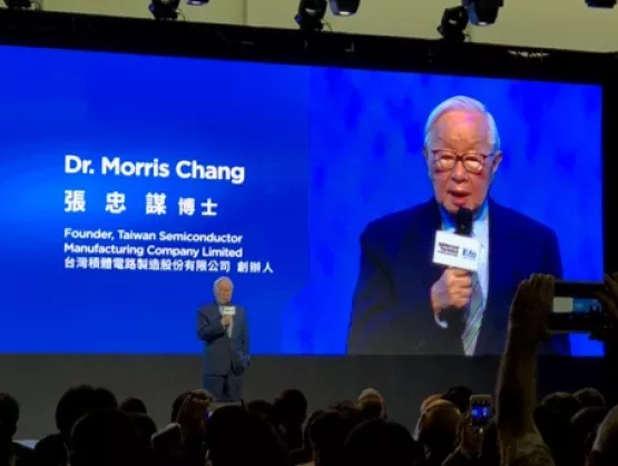
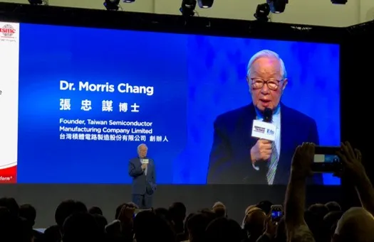
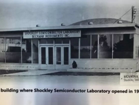
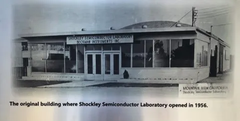
Adapted from the Computer History Museum’s “Celebrating the Birthplace of Silicon Valley” invitation. Work that sowed the seeds of the digital, hyper-connected world we know today all started in a squat, unremarkable building in Mountain View, California. Long before the structure’s foundation was laid, Santa Clara County flourished with orchards, not chips. Between the 1880s and 1940s, eight million fruit trees carpeted Silicon Valley. By 1939, San Jose, with a population of 57,651, was the largest canning and dried-fruit packing center in the world, with 18 canneries, 13 dried-fruit packing houses, and 12 fresh-fruit and vegetable shipping firms*.In 1956, silicon sprouted from new fertile ground.That’s when startup Shockley Semiconductor Laboratory, employing some of the most brilliant young minds in the business, produced Northern California’s first silicon transistor prototypes and formed the technological and cultural bedrock for today’s Silicon Valley.Fed up with William Shockley’s hard-nosed management style, eight Shockley employees – including Gordon Moore, Robert Noyce, Julius Blank, Victor Grinich, Jean Hoerni, Eugene Kleiner, Jay Last, and Sheldon Roberts – resigned in September 1957 and founded Fairchild Semiconductor Corporation. Fairchild was the seedling from which companies valued at over $2 trillion have grown and the source of the integrated circuit “computer chip” that has revolutionized our world.Now, more than 60 years later, the site of Shockley Labs, already an IEEE Historical Milestone, is being formally recognized by the IEEE and the City of Mountain View for its historical significance in a special dedication ceremony on August 15. Thanks to the efforts of many, especially developer Merlone Geier Partners, newly commissioned public sculptures – in the likeness of two early semiconductor devices and a mammoth silicon crystal monument that symbolize the work to come out of the lab – now permanently mark the site, along with various plaques that describe and commemorate the site’s history. The event’s featured speaker is Professor James F. Gibbons, former dean of engineering at Stanford University. Professor Gibbons’ first task at Stanford in 1957 was to work with Shockley and his team to transfer their knowledge of silicon fabrication to Stanford, which could in turn train future engineers for the coming boom in the semiconductor industry. He will share his personal experiences and memories of those early days. Join early semiconductor pioneers, the president of the IEEE, SEMI president and CEO Ajit Manocha and local officials on August 15 to commemorate this legendary Silicon Valley landmark. Guests are invited to enjoy a series of presentations and exhibits and view the stunning sculptures and plaques.The event is free to attend and open to the public. Space is limited so please sign up here to guarantee a seat.Location: 391 San Antonio Road, Palo Alto, California (Phase II of San Antonio Village). Parking is free.*National Park Service, Santa Clara County: California’s Historic Silicon ValleyAriana Raftopoulos is a marketing manager at SEMI.
Read More
The march to greater precision, efficiency and safety – the lifeblood of high-technology manufacturing facilities – has taken on a new urgency as emerging applications such artificial intelligence (AI), the Internet of Things (IoT) and Industry 4.0 give new meaning to smart factories. Facing fiercer competition and ever more sophisticated fabrication processes, semiconductor fabs are under intense pressure to keep pace with new technologies as they work to upgrade. Nowhere are the stakes higher than in Taiwan, where high-tech manufacturing contributes mightily to the region’s GDP growth. To help Taiwan fabs confront the challenges and opportunities of designing smarter factories, SEMI and its High-Tech Facility Committee hosted the High-Tech Facility Workshop in June. SEMICON Taiwan 2018 High-Tech Facility Pavilion exhibitors gathered to explore how they can build smarter factories by deploying smart surveillance and disaster prevention technologies along with smart communications systems that better use manufacturing data to drive new safety and product quality efficiencies.During the workshop, SEMI High-Tech Facility Committee representatives shared strides it has made upgrading overseas facilities and developing standards to help establish smart factories in Taiwan.SEMICON Taiwan – 5-7 September at Taipei’s Nangang Exhibition Center – is also an important event for advancing smart manufacturing in Taiwan. Nearly 30 leading global manufacturers will exhibit at the SEMICON Taiwan High-Tech Facility Pavilion. The venue covers operational aspects of semiconductor manufacturing vital to becoming smarter including energy savings, nano-contamination control, facility information modeling, precision instrumentation and control, fire protection, mechatronics, and automation control. The pavilion will also feature a series of theme events offering a comprehensive overview of topics including the latest practices for integrating smart facility capabilities from the perspective of an advanced fab designer.At the TechXPOT stage, High-Tech Facility Pavilion exhibitors will also demonstrate the latest technology breakthroughs and cutting-edge smart factor solutions.The September 6th High-Tech Facility International Forum at SEMICON Taiwan will again gather factory experts and thought leaders from industry and academia to examine “Effective Ways to Make a Facility Smart.“ Experts from industry heavyweights in the fields of wafer foundry, LCD, memory and semiconductor packaging including TSMC, UMC, Innolux, ASE, Micron Taiwan, Winbond and VIS will offer insights into key areas of high-tech facilities including facility electricity, machinery, water management, vaporization and automation systems. On the same day as the forum, the High-Tech Facility Get-Together and High-Tech Facility VIP Dinner will bring together industry elites, academic professionals, and government officials to explore partnership opportunities. SEMI Taiwan and the High-Tech Facility Committee share HTF market trends information, technology updates and standards with SEMI members and exhibitors. Founded in 2013, the High-Tech Facility Committee now has 85 corporate members. Dedicated to accelerating industry collaboration through the integration of Taiwan industrial, government and academic resources, the committee each year holds several group meetings focusing on topics including energy savings, earthquake and fire protection, nano-contamination control, and precision instrumentation and control to advance critical technologies and facilitate standardization. The committee also aims to help the industry become more competitive faster by promoting technology standards that boost productivity and reduce production costs.Please visit www.semi.org and www.semicontaiwan.org for more information about SEMI’s high-tech facility initiatives.Iris Tsou is a marketing specialist at SEMI Taiwan.
Read More
Two months after opposing $34 billion in U.S. trade tariffs on behalf of the U.S. semiconductor manufacturing industry, Jonathan Davis, global vice president of industry advocacy at SEMI, this week spoke out against an additional $16 billion in duties on Chinese goods. Testifying before the same U.S. interagency panel mulling the tariffs, Davis called for the removal of 29 tariff lines covering items critical to semiconductor manufacturing including machines and spare parts used to make, wafers, flat panel displays and masks.In his testimony to the panel, Davis stressed that while SEMI supports stronger protections against the theft of valuable intellectual property (IP), tariffs do little to address U.S. concerns over IP loss. Over the past month, SEMI has also submitted written comments and opposed the tariffs in public testimony. The panel includes representatives from the U.S. Trade Representative (USTR), Departments of Treasury, Commerce, State and Defense, and the Council of Economic Advisers.Also testifying, Joe Pon, corporate vice president at Applied Materials, explained that the proposed tariffs will harm small and midsized companies and other U.S. business interests. Describing the tariffs as a tax on exports of high-value U.S. goods, Pon said the duties give non-U.S. firms an unfair competitive advantage.In a parallel push to Davis’s testimony, SEMI, with more than 10 representatives from six member companies, met with 16 congressional offices this week to underscore the damage the tariffs would wreak on the U.S. semiconductor industry. The fallout would include higher operating costs, fewer exports and slower innovation. The tariffs would also curb industry growth and put thousands of high-paying, high-skill jobs at risk. SEMI pressed congressional leaders to reject the tariffs and support a push for congress to re-assert itself on trade policy.Tariffs to Cost U.S. SEMI Members More than $500 MillionSEMI estimates that the second list of proposed tariffs, covering about $16 billion in Chinese goods, will cost its 400 U.S. members more than $500 million annually in additional duties.The tariffs on $34 billion in Chinese goods, which took effect July 6, impact products such as test and inspection equipment as well as spare parts that enter the U.S. from China. That round of tariffs will cost SEMI member companies and estimated tens of millions of dollars annually. SEMI Public Policy Team Asks Members to Review Tariff ListLooking ahead, SEMI encourages members to review the newly released $200 billion tariff list, determine any impact to their businesses and share their findings with SEMI’s public policy team.The U.S. Trade Representative (USTR) has published the exclusion process for products subject to the China 301 tariffs. If your company’s products are subject to tariffs, you can request an exclusion.In evaluating product exclusion requests, the USTR will consider whether a product is available from a source outside of China, whether the additional duties would cause severe economic harm to the requestor or other U.S. interests, and whether the product is strategically important or related to Chinese industrial programs (such as “Made in China 2025”).The deadline for submitting product exclusion requests to USTR is October 9, 2018. Approved exclusions will be effective for one year upon approval and retroactive to July 6, 2018.More information including the process for submitting the product exclusion request can be found here.Any SEMI members with questions should contact Jay Chittooran, Public Policy Manager at SEMI, at [email protected].
Read More