downloadGroupGroupnoun_press release_995423_000000 copyGroupnoun_Feed_96767_000000Group 19noun_pictures_1817522_000000Member company iconResource item iconStore item iconGroup 19Group 19noun_Photo_2085192_000000 Copynoun_presentation_2096081_000000Group 19Group Copy 7noun_webinar_692730_000000Path
Skip to main content
Default Banner Image

Business and Markets

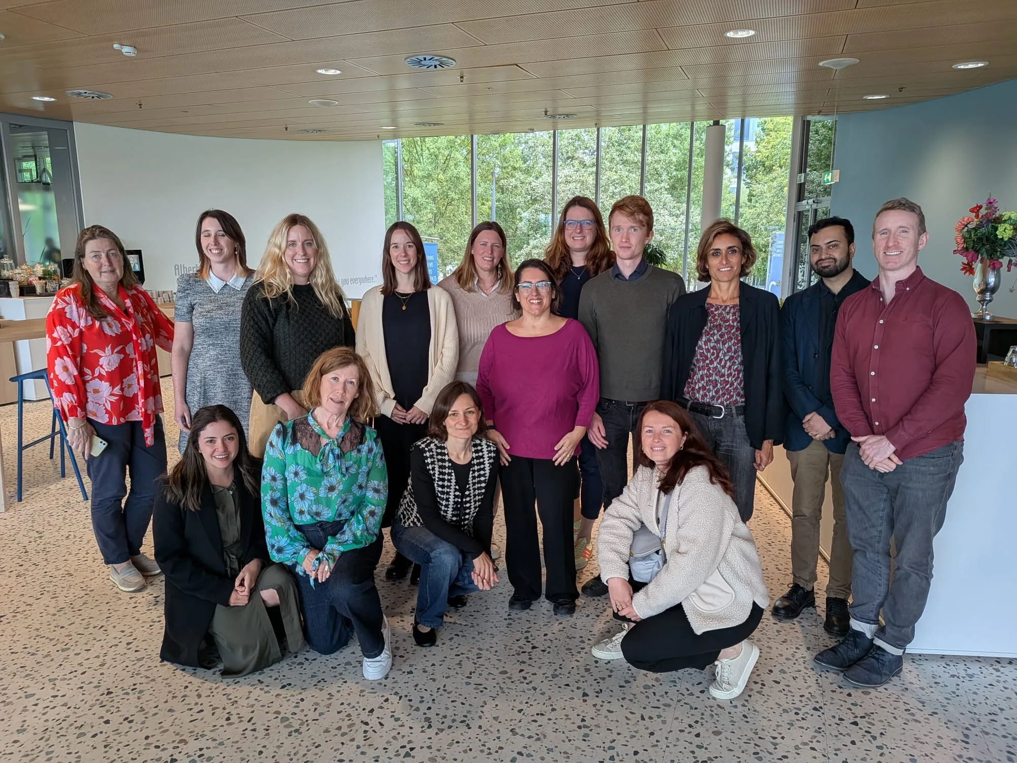
As the semiconductor industry continues to advance, effective quality management is increasingly essential. The SEMI Quality Benchmarking Consortium (QBC) brings together leading companies to exchange best practices, benchmark performance, and promote collective improvement across the global semiconductor landscape. The last QBC meeting was hosted by Bill Lechten of Micron at their headquarters in Boise, Idaho. Representatives from GlobalFoundries, Infineon Technologies, STMicroelectronics, NXP Semiconductors, and Texas Instruments came together for two days of in-depth discussions and knowledge sharing.The session began with an overview of Micron’s global business and manufacturing footprint. The company reported record revenue of $37 billion in 2025 and currently hold more than 60,000 patents. Micron is investing approximately $150 billion in U.S.-based DRAM manufacturing, which is expected to generate around 90,000 direct and indirect jobs. The QBC operates on a “give-to-get” philosophy where members must actively contribute survey responses and participate in open discussions to access shared benchmarking data. This meeting focused on three topics: risk management, customer return, and product change notification. Participants presented their approaches, shared lessons learned, and engaged in roundtable discussions to identify best-known methods and address common challenges. Customer Returns and Failure AnalysisThe group reviewed processes for handling customer returns and failure analysis. Discussions covered escalation protocols, data-driven versus physical failure analysis, sampling strategies, and customer acceptance challenges. Members shared approaches to closure criteria, complaint prioritization, and using FA and complaint data for trend analysis and continuous improvement. Local support models and the balance between cost, proximity, and specialized lab capabilities were also key topics.Product Change Notifications The consortium explored industry-wide PCN practices, focusing on notification volume, approval processes, and customer expectations. Companies highlighted distinctions between PCN (requiring approval) and CIN (informational) and the challenges of handling multiple changes per notification. Participants shared strategies for managing customer approvals, sample delivery, and internal tracking, including phased notifications and customized communication. Standardization efforts were discussed, such as adopting the JDEC XML schema, while balancing operational efficiency with contractual obligations and customer requirements.Risk ManagementMembers discussed structured approaches to quality and qualification risk, including product grade classification and risk assessment methodologies like FMEA and QRA. Emphasis was placed on assessing end-user system complexity, mission profiles, and application-specific requirements, especially for automotive and AI workloads. Organizations shared practices for transparent customer communication, balancing speed and risk, managing residual risk, and integrating qualification with change management. AI and data analytics were highlighted as emerging tools to support predictive risk assessment and continuous improvement.AI and Digitalization in Quality ManagementArtificial intelligence is becoming a growing focus for semiconductor quality teams. Companies shared early-stage AI initiatives. Based on survey results and discussion, consortium members agreed to establish a working group to explore AI uses cases in risk assessment for change management and new product introduction. Looking AheadWith growing complexity in semiconductor technologies, industry collaboration is vital. Through open discussions and benchmarking, the SEMI Quality Benchmark Consortium enables companies to share knowledge, identify best practices, and address common challenges. The consortium will continue its work at the upcoming meeting to be hosted by Texas Instruments in Dallas, Texas. (From Right to Left) – Karim Somani (SEMI), Sarah Shen (SEMI), Mark da Silva (SEMI), Ivo Clerici (GlobalFoundries), Wesley Hirsch (TI), Roberto Lissoni (STMicroelecetronics), Lou Cerra (NXP), Jens Luepke (Infineon), Bill Lechten (Micron), Fern Yoon (Texas Instruments)Sarah Shen is Senior Coordinator, MEMS Sensors Industry Group at SEMI.
Read More
As the global semiconductor industry enters a decisive new phase shaped by artificial intelligence, SEMICON Korea 2026 convened the ecosystem from February 11–13 in Seoul, bringing together the companies, technologies, and talent required to sustain momentum on both sides of the AI equation: using AI to transform semiconductor operations, and advancing semiconductor innovation to enable the next generation of AI systems.At the SEMICON Korea press conference, Hyun Cha, President, SEMI Korea stated that with nearly 550 exhibiting companies and over 2,400 booths, the event underscored how progress now depends on a virtuous cycle of collaboration across the entire value chain—from materials and equipment to design, manufacturing, packaging, and systems integration.Opening Perspectives: Collaboration as the Catalyst In the opening ceremony, Ajit Manocha, President and CEO of SEMI, framed the opportunity and challenge ahead: AI is accelerating the industry’s trajectory toward a trillion-dollar market, but sustaining that growth will require deeper collaboration across an increasingly complex ecosystem.That message was reinforced by YH Lee, Chairman of Wonik, who emphasized the need for alignment across the value chain, “looking side to side, not only forward,” as scaling semiconductor technologies grows more difficult. From a policy perspective, Shinhak Moon, Vice Minister of Korea’s Ministry of Trade, Industry Resources (MOTIR), highlighted the importance of the full ecosystem, including parts, materials, and equipment, while cautioning that resilience will be critical amid economic cycles. Together, these perspectives set the stage for a keynote program focused on how AI and semiconductors are now co-evolving.Opening Keynote: Samsung Electronics on Architecting the Future of AI SystemsThe keynote program opened with Jaihyuk Song, Corporate President and CTO of Samsung Electronics, who examined what comes next for AI systems as compute and memory demands rise exponentially. He described a widening gap between compute performance and memory bandwidth, positioning advanced packaging and architectural innovation as central to closing that gap.Song outlined Samsung’s focus on next-generation memory technologies, including high-bandwidth memory and compute-in-memory approaches, as well as the transition beyond traditional Moore’s Law scaling toward planar, vertical, and stacked architectures. His message was clear: sustaining AI performance gains will depend on tight integration across design, process technology, packaging, and system architecture, reinforcing the need for ecosystem-wide coordination. ASE: From Chip Integration to System OptimizationTien Wu, CEO of ASE, expanded the discussion from devices to systems, arguing that advanced packaging has become a primary driver of system-level performance and efficiency. As AI workloads push power, thermal, and bandwidth limits, Wu described a shift from single-chip packages toward heterogeneous integration, 2.5D and 3D architectures, and co-packaged optics.Wu emphasized that productivity, yield, and throughput will increasingly determine competitiveness as packages grow larger and more complex. His perspective reinforced a central theme of SEMICON Korea 2026: AI-driven demand is forcing tighter coupling between design, manufacturing, and packaging, making collaboration not optional, but essential.Cadence: AI-Enabled Design Across the Value ChainBoyd Phelps, Senior Vice President and General Manager of Silicon Solutions at Cadence Design Systems, highlighted how AI is already reshaping semiconductor design and development. As process scaling slows and cost per transistor rises, Phelps described disaggregation and chiplets as a new abstraction layer that enables continued innovation through customization and configurability.He also pointed to the growing role of AI-driven design automation, noting that a significant portion of recent designs leveraged AI-enabled tools. Cadence’s end-to-end portfolio—from IP and tools to packaging and test—illustrated how AI is becoming both a design accelerant and a necessary response to rising system complexity, reinforcing the industry’s virtuous cycle.Lam Research: Velocity Through AI and AutomationThe theme of operational transformation took center stage with Tim Archer, President and CEO of Lam Research, who introduced “velocity” as the defining imperative of the AI era. As AI-driven demand accelerates product cycles and increases complexity, Archer argued that speed must be matched with direction—enabled by AI, automation, and digital twins.Archer detailed Lam’s progress toward autonomous fabs, equipment intelligence, and collaborative virtual development environments that reduce variability and accelerate process development. These capabilities, he explained, allow the industry to respond faster while preserving quality and resilience—another example of AI improving semiconductor operations even as semiconductor innovation enables AI growth.SK hynix: AI as a Tool for Memory InnovationLooking further into the future, Sunghoon Lee, Senior Vice President and Head of R D Process at SK hynix, addressed the mounting difficulty of sustaining memory technology cadence. As stacking, bonding, and material challenges intensify, Lee described a shift toward AI-based R D models that dramatically accelerate material discovery and optimization.By integrating AI into material exploration and process development, SK hynix is shortening development cycles and enabling new memory architectures. Lee emphasized that realizing the full potential of AI-driven R D will require greater data sharing and collaboration across partners—reinforcing the ecosystem-wide virtuous cycle.NVIDIA: From Chips to AI InfrastructureThe final keynote, delivered by Soyoung Jeong, Head of Korea Business at NVIDIA, framed the transformation of NVIDIA from a GPU company into an AI infrastructure provider. He described how accelerated computing and AI factories are reshaping chip design, manufacturing, packaging, and system integration.From AI-assisted design and simulation to system-level optimization and physical AI, NVIDIA’s approach illustrated how semiconductors and AI are now inseparable, each advancing through the other. Partnerships across memory, equipment, and software ecosystems were highlighted as critical to sustaining this momentum.A Program Aligned Around the Same ThemeBeyond the keynotes, SEMICON Korea 2026 reinforced these messages through technology symposia, AI and smart manufacturing forums, cybersecurity discussions, and workforce development initiatives—all focused on enabling AI-powered innovation across the semiconductor lifecycle.Additional Program Highlights: Extending the Virtuous Cycle Across the EcosystemBeyond the keynote stage, SEMICON Korea 2026 reinforced the same virtuous cycle of AI and semiconductor innovation through a wide range of technical, business, and workforce programs designed to engage every layer of the value chain.AI Summit: Translating Strategy into Industrial ImpactThe AI Summit, co‑hosted by SEMI and KAIST, served as a focal point for aligning academic research, device manufacturers, and equipment leaders around AI-powered industrial innovation. Featuring faculty from KAIST alongside representatives from Samsung Electronics, SK hynix, and global equipment companies, the summit explored technology strategies and future roadmaps aimed at accelerating AI adoption across semiconductor manufacturing and design.The discussions reinforced a central theme of SEMICON Korea 2026: AI is no longer an isolated software layer, but a system-level capability that must be embedded across processes, tools, and infrastructure to unlock its full value.Smart Manufacturing Forum: Advancing the Autonomous FabThe Smart Manufacturing Forum highlighted how AI, digital twins, and real-time data are transforming semiconductor fabs toward more autonomous, resilient operations. Speakers shared trends and success cases demonstrating how advanced analytics and AI-driven decision-making are improving yield, productivity, and operational agility.This forum echoed themes raised by equipment and manufacturing leaders in the keynote program, underscoring how AI-driven manufacturing excellence is becoming a prerequisite for meeting the speed, scale, and quality demands of next-generation AI chips.Startup Summit: Fueling Innovation from the Ground UpThe Startup Summit showcased emerging semiconductor and display startups focused on applying AI to improve chip performance, energy efficiency, and manufacturing processes. By connecting startups with industry leaders and venture capital firms—including Applied Ventures, Intel Capital, Samsung Ventures, and SK hynix—the summit emphasized the importance of nurturing innovation across the ecosystem.These early-stage technologies represent the next wave of ideas feeding into the virtuous cycle, where AI-enabled innovation at the startup level can scale rapidly through collaboration with established players.Cybersecurity Forum: Securing the AI-Driven Semiconductor FutureAs AI becomes deeply embedded in semiconductor operations and data flows, the Cybersecurity Forum addressed the growing need for digital trust across the ecosystem. Global experts examined cybersecurity challenges related to compliance, fab security, and AI data governance, highlighting the importance of collaboration to protect sensitive data and intellectual property.The forum reinforced that secure, trusted infrastructure is a foundational requirement for the AI-driven transformation discussed throughout SEMICON Korea 2026.Conclusion: Advancing TogetherSEMICON Korea 2026 made clear that the next phase of industry growth will not be driven by isolated breakthroughs, but by a virtuous cycle of alignment across the full semiconductor value chain. By integrating AI into design, manufacturing, and operations—and by advancing semiconductor technologies that power AI—the industry is building a foundation for sustained innovation. As the event demonstrated, progress will be fastest when the ecosystem moves forward together.Samer Bahou is Director, Corporate Communications at SEMI. Jaegwan Shim is Senior Specialist, Marketing at SEMI Korea.
Read More
The semiconductor industry is the bedrock of modern technology, enabling everything from AI and cloud computing to electric vehicles. Yet, this critical sector is also one of the most resource-intensive globally, with a substantial dependency on water. A single fabrication plant can demand up to 10 million gallons of water daily, comparable to the consumption of a city with 300,000 residents. Much of this water is, of course, reused and recycled through sophisticated systems. This immense water usage, particularly the requirement for ultrapure water for processes like cleaning and etching, makes consistent access to high-quality water a non-negotiable for operational reliability and business continuity. The new insights report "Ripple Effects: Water Risk and Resilience Across the Semiconductor Value Chain" provides the first global baseline of water risk hotspots for the semiconductor sector, assessing water risks across 140 facilities across 89 water basins to inform future risk mitigation strategies.The analysis discusses how water risk can manifest itself as a financially material impact on business continuity by triggering idle time, recovery costs, and cascading delivery delays across global supply chains. S P Global projects that by 2050, water-related risks could cost the world's largest IT companies up to $24 billion annually. Crucially, the study identified flooding and reputational risks—such as strained relationships with local communities over water allocation—as the most significant immediate threats to the semiconductor value chain. These concerns are most acute in major hubs like Taiwan, South Korea, and parts of the U.S.While the industry is frequently criticized for its water usage, only 16% of the analyzed sites are currently affected by water scarcity. However, this metric offers a false sense of security. As climate change intensifies, the frequency and severity of water-related disruptions are set to exceed the scope of existing contingency plans. The long-term projections show that over 40% of semiconductor facilities announced since 2021 are located in watersheds projected to face high or extremely high water stress between 2030 and 2040. This underscores the urgent need to integrate forward-looking risk modeling into new site planning to ensure long-term operational resilience.Effective risk management is significantly hindered by the limited transparency surrounding supplier-level water data. While many companies perform water assessments for their direct operations, a comprehensive, industry-wide approach to supplier data and risk management is lacking. CDP data shows that 1 in 5 companies reported $77 billion under threat from supply chain water risks, yet only half of those companies engage with their suppliers on these issues. For semiconductor end users, these risks are often deep within multi-tiered networks, requiring engagement that goes well beyond Tier 1 suppliers.To manage these complex risks, the report stresses the necessity of moving toward a contextual approach that includes localized assessments. Contextual water risks are inherently location-specific, dependent on local availability, quality, and infrastructure, as well as broader catchment-level dynamics, regulatory pressures, and community expectations. Several structured methodologies support this necessary shift from basic operational management to corporate water stewardship, including the Alliance for Water Stewardship (AWS) Standard, the TNFD's LEAP framework, and the Science Based Targets for Nature (SBTN). This approach encourages companies to look beyond their own operations to safeguard regional water security.Because water is a shared resource, collective action is essential to deliver the scale and urgency needed to tackle common challenges within catchments. The semiconductor value chain is deeply interconnected, with companies often sharing suppliers within the same water basins, creating a strategic opportunity for collaborative stewardship. The report encourages companies to scale their impact by moving beyond isolated efforts to form sector-wide and cross-sector partnerships—especially at the catchment level—through public-private engagement. This collaboration, which includes proactive engagement with policymakers and local utilities, is key to aligning on water management and stewardship practices to address shared water challenges and build collective trust.Innovation and technology must play a central role in advancing water stewardship across the value chain. A major hurdle is the general undervaluation and mispricing of water, which perpetuates systemic underinvestment in water-focused technology. Despite this, leading semiconductor companies are deploying advanced solutions such as onsite recycling systems, real-time water monitoring, and utilizing alternative sources like municipal wastewater. Embracing AI-driven systems for scenario modeling and catchment-level risk forecasting further enhances adaptive capacity and resilience.The "Ripple Effects" report makes it clear that water challenges affect every segment, demanding tailored response tactics and strategies. Foundries, with their large operational footprints, must prioritize sourcing reclaimed water and expanding onsite reuse, while chemical and materials suppliers must proactively manage rising regulatory risks around water quality contaminants. The insights report also provides a practical roadmap for advancing corporate water stewardship, outlining progression from water risk assessment (Stage 1) to site-level action and collective engagement (Stage 2), and culminating in transparent validation and reporting (Stage 3). By following a structured water stewardship pathway, the semiconductor industry can build operational resilience and ensure a responsible future for the entire value chain.To learn more, download the report or watch the webinar recording. Alua Suleimenova is Senior Program and Staff Manager | Global Sustainability at Marvell Technology and leader of SEMI's ERMR Working Group.The Environmental Risk Mitigation and Reporting (ERMR) Working Group was established under SEMI's Sustainability Initiatives in January 2023, and it aims to develop a baseline and roadmap of best practices for identifying, managing, governing and reporting climate, water, and biodiversity risks across the semiconductor value chain. This insights report is a publication in SEMI’s ERMR Working Group thought‑leadership series on global environmental risks and resilience.
Read More
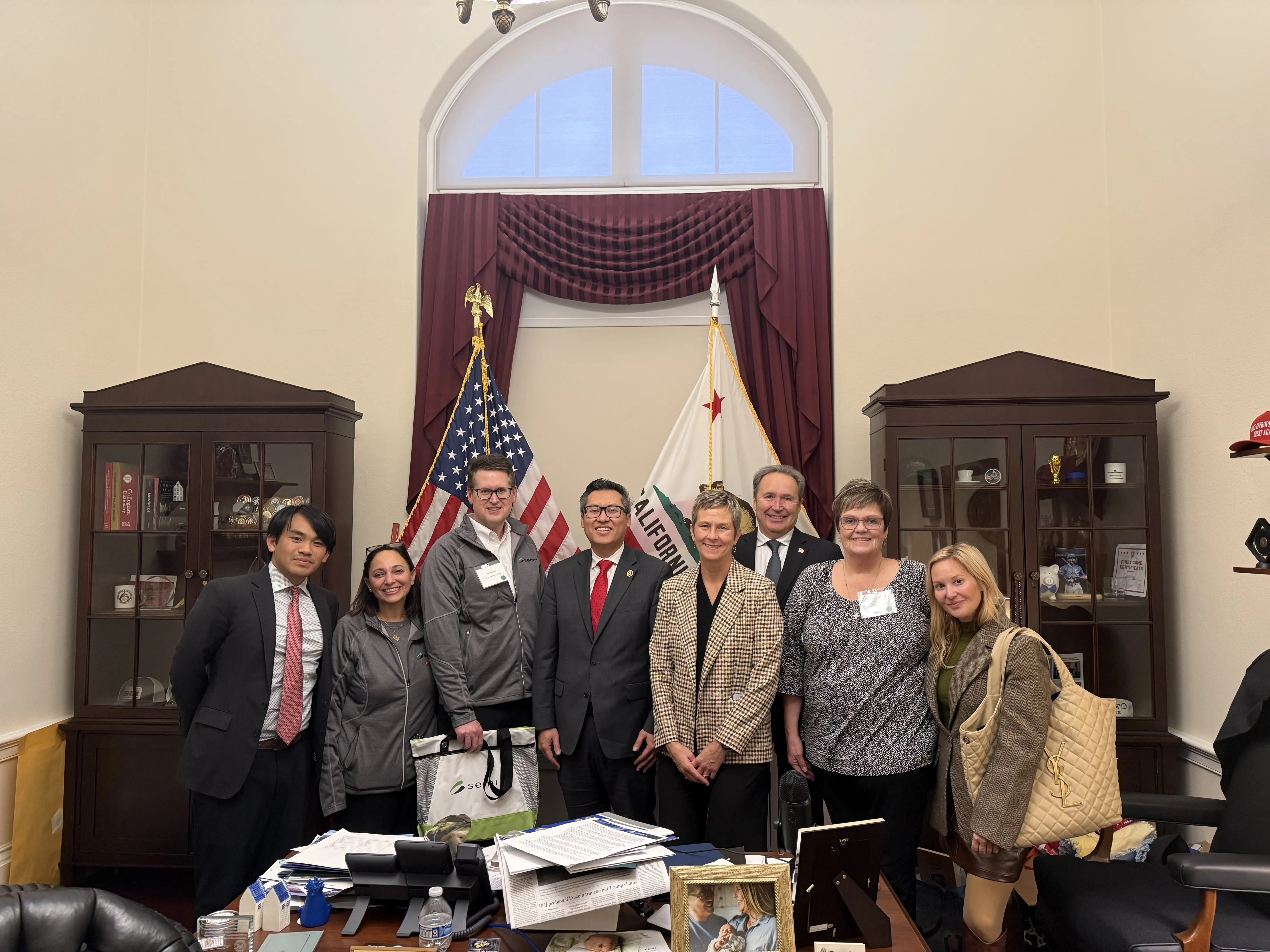
Hosted by the SEMI North America Advisory Board (NAAB), executives from member companies across the semiconductor supply chain with operations in the U.S. recently convened in Washington, D.C. to advocate for the policies most critical to semiconductor competitiveness and national security. From March 3-5, 2026, SEMI executives and more than 80 representatives from member companies embarked on Capitol Hill, engaging directly with members of Congress and federal officials to advance the industry’s top policy priorities heading into 2026. These industry leaders from across the semiconductor ecosystem—from materials and equipment suppliers to chipmakers and end users—underscored the urgent need for industry-informed policymaking. Focus topics included:• Trade and Tariff Policy – Promote a balanced trade policy that preserves market access and avoids overlapping tariffs on the same product, as well as narrowly tailored, coordinated export controls to protect national security without harming U.S. competitiveness.• Tax Policy and Investment Incentives – Establish a competitive tax framework would reward innovation and lock the next generation of semiconductor production onto U.S. soil.• Research and Development (R D) Investment – Invest in long-term tax and R D incentives to sustain semiconductor investments.• CHIPS and Science Act Implementation and Beyond – Continued implementation of the CHIPS Act and related programs and develop a forward-looking initiative or roadmap to continue the industry’s momentum.• Workforce Development – Establish a national workforce pipeline aligned with federal, state, and industry programs to meet critical talent needs.• Environmental Regulations – Support pragmatic policies that balance environmental goals with innovation. The semiconductor industry is vital to every facet of our lives today from artificial intelligence and advanced manufacturing to healthcare. The U.S. leads in semiconductor design and advanced technologies that enable the AI era—and clear, predictable policy frameworks are critical to the Administration’s goals around maintaining U.S. technological leadership and advancing national and economic security.A highlight from the Fly-In was recognizing Indiana Senator Todd Young with the SEMI Americas Government Leadership Award on March 4. The NAAB selects Government Leadership Award honorees based on their impact on policies and incentives to bolster semiconductor design and manufacturing and advance the growth of the global industry. SEMI member companies are making record level investments in the U.S. semiconductor ecosystem, bringing high-paying, skilled jobs to communities across the country. This year’s Fly-In participants met with over 100 key congressional offices and committees and engaged directly with administration officials to discuss policies that support economic growth, innovation, and national security. Through collaboration, credibility, and consistent engagement, SEMI looks forward to continuing to work with Congress and the administration to ensure the next phase of U.S. semiconductor expansion delivers lasting benefits for the U.S. economy. Visit SEMI Global Advocacy to learn more about public policy efforts and developments as well as how your company or organization can get involved.Learn more about the SEMI Public Policy and Advocacy program and the 2026 policy strategy: https://www.semi.org/en/global-advocacy.Christina Banoub is Senior Manager, Federal Affairs at SEMI.
Read More
In the summer of 2025, I had the privilege of leading more than a dozen SEMI Foundation STEM summer camps in schools across multiple communities.Each camp brought students face-to-face with hands-on engineering challenges, semiconductor learning modules, and conversations about the careers connected to what they were building.What stood out most wasn’t just the energy in the classrooms; it was the moment students began to see themselves in futures they hadn’t previously imagined. For many, it was their first exposure to the semiconductor industry. Their first time hearing about advanced manufacturing careers. Their first time understanding that a certificate, credential, or engineering degree could lead to a stable, high-quality job shaping the technologies that power modern life.And it reinforced something we believe deeply at the SEMI Foundation, that workforce development does not begin at graduation; it begins in grade school with early awareness and intentional exposure.Starting Earlier: Where the Semiconductor Workforce Truly BeginsBuilding a strong, future-ready semiconductor workforce does not begin in college, or even high school. It begins in the earliest years of science, technology, engineering, and mathematics (STEM) exposure.Since 2003, I have created STEM programming that introduces college majors and career pathways to K–12 students. At the SEMI Foundation, that work now connects directly to one of the most urgent workforce challenges of our time, ensuring the semiconductor industry has the skilled talent needed to support domestic manufacturing expansion and global competitiveness.When elementary and middle school students engage in hands-on STEM experiences, they build confidence. They develop technical vocabulary, critical thinking skills, and resilience. They begin to understand how the devices they use every day are designed and manufactured. That early spark matters, especially in industries like semiconductors, where awareness has historically been limited among younger students.Moving From Exposure to Industry ExplorationAs students progress, programming must move from exposure to exploration.Through SEMI Foundation initiatives, including hands-on camps, classroom modules, and industry-connected programming, students begin to see how semiconductors power everything from smartphones and AI to healthcare systems and clean energy technologies.Middle school and early high school programs should intentionally connect STEM learning to real-world applications:Engineering design challenges tied to semiconductor conceptsProject-based learning informed by industry practicesCareer speakers from manufacturing and technical rolesMentorship that reflects diverse entry points into the industryThis stage is critical for workforce development. Quality hands-on learning must be paired with representation and mentorship. Students need to hear authentic stories about different pathways into technical fields, whether through two-year degrees, apprenticeships, industry certifications, or four-year engineering programs.High School: Where Awareness Becomes PreparationHigh school is where exploration must transition into preparation.Structured career pathways, dual enrollment opportunities, industry certifications, internships, and apprenticeship models create tangible bridges between classroom learning and workforce entry.When students graduate with credentials aligned to high-demand sectors, including advanced manufacturing and semiconductor production, they leave with more than knowledge. They leave with validated skills and industry relevance.This alignment does not happen by accident. It requires coordinated partnerships between K–12 systems, higher education institutions, workforce agencies, and employers. At the SEMI Foundation, we work to support this alignment so curriculum reflects industry needs and students experience clear, navigable pathways into careers.When education and industry move in sync, skills gaps narrow, and regional economies strengthen.Sustaining Momentum: Postsecondary and Employer PartnershipPostsecondary institutions and employers play a pivotal role in sustaining momentum.Stackable credentials, registered apprenticeships, and paid work-based learning models allow students to build competencies while earning income. Clear articulation agreements between high schools, community colleges, and universities reduce talent loss and create seamless transitions. In the semiconductor industry, where technical precision and specialized skills are essential, these structured pathways are not optional. They are foundational.A Long-Term Vision for Semiconductor Workforce GrowthThe semiconductor industry powers nearly every aspect of modern life. But sustaining that innovation requires long-term workforce vision. The students I met in our 2025 summer camps reminded me of what is possible when exposure meets opportunity.When we start early, align intentionally, and collaborate across systems, we do more than prepare a workforce. We cultivate the next generation of innovators who will design, build, and lead the technologies shaping our future.Bia Hamed is Program Manager, Global Education Initiatives at the SEMI Foundation.
Read More
On February 20, the U.S. Supreme Court ruled that the International Emergency Economic Powers Act (IEEPA) does not authorize the use of tariffs, invalidating certain tariffs imposed by the Trump Administration under the statute.SEMI shared the following statement on the ruling: SEMI acknowledges today’s U.S. Supreme Court ruling regarding the use of tariffs under the International Emergency Economic Powers Act. As the implications of the decision become clearer, we welcome further guidance and remain committed to working with the U.S. government to strengthen semiconductor supply chains, support innovation, and expand domestic chip manufacturing.Continued investment in U.S. manufacturing depends on stable, reliable access to the highly specialized equipment, materials, and components essential to semiconductor production. Driven by global demand, breakthrough innovation, and record levels of investment, the semiconductor industry is projected to reach a $1 trillion market this year. Clear, consistent, and predictable trade policy remains critical to providing manufacturers – particularly small- and medium-sized enterprises – the certainty necessary to sustain long term investment, scale production, and reinforce technological leadership in the United States.Visit SEMI Global Advocacy to learn more about public policy efforts and developments as well as how your company or organization can get involved.Royal Kastens is Vice President, Global Public Policy Advocacy at SEMI.
Read More
When most people hear “semiconductors,” they think of something abstract: tiny chips, complex equations, cleanrooms hidden behind glass. Relevant, sure, but distant. Compare that to professions like architects or doctors. We can picture their training. We understand their impact. We see a clear path from curiosity to contribution. The semiconductor industry deserves the same clarity and more. Because semiconductors don’t just power devices. They power progress. The semiconductor industry plays a crucial role in sustaining modern life and will remain instrumental in the future. We know this all too well because most of us work within this industry. It isn’t abstract or difficult for us to see how we fit into the grand scheme of this critical industry. It is important to reflect on our initial motivation for entering this field. The technological advancements we are currently developing were likely beyond consideration when we began our careers. Historically, we’ve done a great job of explaining how someone becomes a doctor or an architect: education, residency or apprenticeship, specialization, growth. The semiconductor industry can and must do the same.Imagine clearly mapped pathways that show:High school students how math, science, and technical programs connect to real semiconductor jobsCommunity college and university students how internships, co-ops, and labs translate into manufacturing, design, or research rolesCareer-changers and Veterans how reskilling programs, certifications, and on-the-job training can open doors without starting overWhen people can see the steps, the industry becomes less intimidating and far more inviting.Introducing ChipPathThis is where the SEMI Foundation’s newest platform, ChipPath, comes in! ChipPath, powered by the National Network for Microelectronics Education (NNME) , makes it easier for individuals to understand where they fit today and where they can grow tomorrow. “ChipPath marks a major step forward in our mission to connect people to opportunities in the semiconductor industry,” said Shari Liss, Vice President of Global Workforce Development and Initiatives at SEMI. “By combining career exploration, education pathways, and live job data into one platform, we’re not just helping individuals find jobs, we’re helping them build lifelong careers that drive innovation and impact.”ChipPath helps users explore roles across the semiconductor ecosystem, not just by job title, but by skills, interests, and pathways. A student interested in problem-solving, automation, or precision work can see how those interests translate into manufacturing, technician, or engineering support roles. A career-changer with experience in logistics, quality, or data analysis can quickly identify how their existing skills map to in-demand semiconductor jobs.This shift from “Do I belong here?” to “I can see myself doing this” is foundational. When people can visualize a role that fits them, they are far more likely to pursue it with confidence.Perhaps most importantly, ChipPath doesn’t end with exploration and preparation, it connects talent to actual job openings across SEMI member companies. By serving as a shared access point between job seekers, educators, training providers, and employers, ChipPath strengthens the entire talent ecosystem. Candidates gain visibility into opportunities they may never have discovered on their own. Employers gain access to a broader, more diverse, and better-prepared pool of talent aligned to semiconductor workforce needs.This connection transforms workforce development from a fragmented effort into a coordinated system; one where awareness, training, preparation, and hiring reinforce one another.Access for job seekers doesn’t end once they apply. ChipPath includes resources that help them prepare for the next critical step: the interview. Through guidance on interviewing expectations, communication, and workplace readiness, ChipPath helps candidates show up informed, confident, and prepared to engage. This preparation reduces anxiety for candidates and increases the likelihood of successful matches for employers.When candidates understand how to talk about their skills, experiences, and potential in industry-relevant terms, interviews become more productive, and hiring decisions become clearer.For employers, ChipPath is more than a platform, it has the potential to be a workforce multiplier. It reduces friction for job seekers, improves candidate readiness, and helps align skills with real demand across the industry. By leveraging ChipPath alongside outreach and engagement strategies, employers can help create a talent journey that is easier to navigate, access, and succeed in.When people can see where they fit, understand how to prepare, and connect directly to opportunity, the semiconductor industry becomes within reach.Job seekers today want and need more than just a salary; they want meaningful work and pride in what they do. Our industry offers these opportunities, but we must guide them to find it.Visit http://nnme.org/chippath to explore the platform, build your profile, and take your first step toward a future in semiconductors.Melinda Gomez is Program Manager, Veteran Initiatives at the SEMI Foundation.
Read More
Cybersecurity vulnerabilities within the semiconductor supply chain are a growing concern, ranging from individual threats to whole supply chain cyber resilience. It is imperative that the semiconductor industry addresses these risks. Last year, the Semiconductor Manufacturing Cybersecurity Consortium (SMCC) at SEMI introduced Semiconductor Supplier Cybersecurity Assessment (SSCA), providing a streamlined framework allowing suppliers to complete one standardized questionnaire to comply efficiently. The assessment process involves suppliers presenting evidence to support their claims of security controls and measures put in place. Such a body of evidence is critical to establish confidence in the suppliers’ ability to manage risk and comply with standards. The SSCA is a free, open-access resource for the semiconductor industry. This is intentionally made openly available to support SMCC’s mission to strengthen cybersecurity across the semiconductor manufacturing ecosystem. The questionnaire aligns with the six functions of the National Institute of Standards and Technology (NIST) cybersecurity framework 2.0: Govern, Identify, Protect, Detect, Respond and Recover. A recent project led by Swansea University’s Systems Security Group (SSG), in close collaboration with SEMI SMCC, is mapping the evidence requirements necessary for SSCA assurance. The project is funded by the UK Research and Innovation (UKRI) as part of seed funding to support UK/US/Germany collaborative research and innovation projects in the field of semiconductor security. UKRI supports such collaboration in the interest of “maintaining confidence in security throughout the design and manufacturing processes,” and particularly to support research addressing “what tools and techniques could help to reduce the risks associated with third-party hardware design and manufacturing services?”.The project ensures that the global ecosystem is engaged so that evidence requirements developed are acceptable, cost-effective, in line with the latest standards and practice, and ultimately suitable for adoption. As part of this project, two workshops are being organized, one in Germany at Bavarian Chip Alliance, Nuremberg on Tuesday, March 10 and one in the UK at Swansea University on Thursday, March 12, aiming to introduce SSCA and the evidence requirements, gather feedback and inspire early adoption. Join either of these workshops to help shape the evidence requirements and help prepare for effective supply chain security assurance. Participants must download the SSCA framework prior to the workshop.Register for the Germany Workshop on March 10Register for the UK Workshop on March 12Key TopicsIntroduction to Semiconductor Manufacturing Cybersecurity Consortium (SMCC)Standardized Semiconductor Cybersecurity Assessment (SSCA)Supply chain assurance and evidence mappingGroup discussion to feedback on evidence requirementsOpen Q A with cybersecurity and compliance expertsWho Should AttendCybersecurity and compliance professionalsSemiconductor suppliersLegal and regulatory affairs professionalsFabless chip designers and foundriesTesting, packaging, design software, R D tools and IPManufacturing/assembly equipment and ancillary fab servicesIntegrated device manufacturersAbout the authors:Siraj Shaikh is a Professor in Systems Security at Swansea University (UK). His research interests lie at the intersection of cybersecurity, systems engineering, and computer science addressing cyber-physical systems security for automotive and transport systems. He is also Co-Founder and Chief Scientist at CyberOwl, which is dedicated to risk analytics and security monitoring for the maritime sector.Mayura Padmanabhan is a Technical Project Manager at SEMI who manages the Cybersecurity Technology Coalition and Traceability activities.
Read More
The semiconductor industry is expanding at an unprecedented pace. Global semiconductor revenues are now forecast to exceed $1 trillion annually by 2030, yet recruitment is struggling to keep pace with the demand for new workers. This is why talent development is a critical focus for SEMI and the SEMI Foundation.Young professionals and students are crucial stakeholders of future talent. Held during SEMICON Europa, Building the Talent Pipeline event provided a showcase for some of Europe’s most enthusiastic promoters of careers in the industry: the Student Ambassadors of the European Chip Skills Academy (ECSA). The session opened with Andra Bornea, a Master’s student of electrical engineering at the Technical University of Cluj-Napoca in Romania, who shared the inspiring story of her journey towards a career in electronics. “For me, it started when I attended the ECS Summer School in 2023 along with 39 other students. It was a life-changing experience,” Bornea shared.The Summer School is a week-long programme jointly organised by AENEAS, ECSA, EPoSS and Inside, bringing together lectures, demonstrations and interactive sessions that give students a first-hand glimpse into what a career in semiconductors can look like. For Bornea, the impact was immediate and decisive. “Attending the Summer School convinced me to shift the focus of my studies from telecommunications and pursue a Master’s in electrical engineering,” she added. Today, Bornea is one of 70 students across Europe who form the ECSA Student Ambassador Programme, a community she describes as “a vibrant network of motivated students working towards the goal of keeping Europe at the forefront of the global semiconductor industry.”Andra Bornea, Technical University of Cluj-Napoca The event also featured other ECSA student ambassadors who are actively promoting the semiconductor industry within their own academic communities. One of them was András Bálint Mészáros, an electrical engineering student at the Budapest University of Technology and Economics, who spoke about his determination to build a student electronics club despite facing administrative hurdles along the way. Reflecting on the process, Mészáros said, “ECSA provided good opportunities to start a community of students interested in observing how the microelectronics industry works.”András Mészáros, Budapest University of Technology and Economics A similar spirit of initiative was shared by Nassim Beladel, a Master’s student at ETH Zurich, who described founding Young Neuromorphs which is a student association focused on computational hardware design inspired by the structure of the human brain. Beladel outlined ambitious plans for the group, including an FPGA hackathon in 2026 supported by the Edge AI Foundation, as well as a proposal to present the association’s work at an IEEE event in Shanghai. Nassim Beladel, ETH Zürich These new initiatives supplement a vibrant network of clubs and events around Europe. Octavian-Constantin Axinte, a Master’s student at the Technical University of Cluj-Napoca, told the forum of a Romanian competition for electronics students which has its roots way back in 1992. The Technologies of Interconnections in Electronics (TIE) contest attracted 1,500 students to its final stage in 2025. Axinte said that the benefits of participation included “hands-on experience of professional work, interaction with teachers, and, if all goes well, a job offer!” Octavian Axinte, Technical University of Cluj-Napoca Pioneering Research Efforts of the Next Generation of Students The Building the Talent Pipeline event also gave ECSA student ambassadors an opportunity to describe the findings of research projects that they have undertaken. Laura Sondakh, a Master’s student at Ghent University, presented her research into the environmental and social impacts of tantalum and cobalt which are critical minerals used in electronic components such as capacitors. “These minerals mostly come from the Democratic Republic of Congo, a country which ranks very low on development indices,” she explained, noting that many mines are located in conflict-affected regions in the east of the country. Laura Sondakh, Ghent University Vuk Vulević, a Bachelor’s student of telecommunications and IT at the University of Belgrade, shared his work on the applications of quantum computing, highlighting its potential beyond classic engineering uses such as machine learning. He explained how quantum technologies could also be applied “in pharmacology, for simulating complex molecules and testing compounds virtually, and in finance, for performing risk analyses and Monte Carlo simulations at high speed.” Vuk Vulević, University of Belgrade Z Zainab, a Research Assistant at Hochschule Anhalt, shared insights from her research into how mechanical strain can be introduced during the wafer saw-dicing process which is a critical step in turning wafers into individual chips. Using Raman spectroscopy, her work helps identify how key process parameters influence wafer integrity, enabling manufacturers to better optimise dicing conditions and reduce hidden damage that can affect chip reliability and manufacturing efficiency.Z Zainab, Research Assistant, Hochschule Anhalt Future Plans for Building the Talent Pipeline The event concluded by looking ahead at how SEMI and its partners are scaling up programmes to support talent development worldwide. Victoria Cummings, Senior Manager for Workforce Development and EU Projects at SEMI Europe, introduced Reinforcing Skills in Chips Design for Europe (RESCHIP4EU), a Master’s program for training the next generation of semiconductor designers supported by SEMI Europe and STMicroelectronics. Outlining the project’s ambition, Cummings said, “The program has a broad curriculum, covering everything from silicon chips and SoCs to safety-critical software, how to run a team, and how to start a semiconductor business.” Victoria Cummings, Senior Manager, Workforce Development and EU Projects, SEMI Europe The focus then shifted towards engaging younger learners. Marco van Schagen and Tijl Bouman, co-founders of JuniorIOT, unveiled their newest workshop, Chips in Schools, which builds on their work to spark interest in electronics among younger students. During a hands-on demonstration, audience members of all ages were invited to examine LEDs under a microscope, learning how different chips can be identified and classified by function.The Chips in Schools workshop will soon be available on the ECSA e-learning platform as part of the ongoing collaboration between ECSA and JuniorIOT. Reflecting on the importance of early engagement, van Schagen noted: “When we talk about the talent pipeline, we need to ask where this pipeline really begins. For us, it’s so important that we reach out to children early to foster their sense of curiosity and discovery.”Marco van Schagen, Co-founder of JuniorIOT, demonstrating the Chips in Schools workshop with Victoria Cummings.Rounding off the session, Mike Glavin, Program Director for Workforce Development at the SEMI Foundation, spoke about efforts to significantly scale the foundation’s impact. He described how, despite hundreds of individual microelectronics education initiatives across schools and colleges in the United States, their collective impact has often been limited by fragmentation and a lack of coordinated promotion. To address this, Glavin introduced the National Network for Microelectronics Education (NNME), an initiative designed to unify and amplify existing programmes by connecting educators, students and regional partners. The goal, he explained, is to build scalable, sustainable talent pipelines: “We want to answer the questions, how do we train teachers to educate students about semiconductors? How do we connect to networks through which we can train educators at scale? And how do we develop resources so that a university can host its own semiconductor day, rather than requiring the SEMI Foundation to put it on?” Mike Glavin, Program Director for Workforce Development, SEMI Foundation From university labs to industry-aligned Master’s programs, the message at SEMICON Europa 2025 was clear: talent development is critical to sustaining Europe’s semiconductor ambitions. SEMI would like to thank its partners across academia and industry, as well as the vibrant community of ECSA Student Ambassadors, whose collaboration, commitment and creativity are helping to build a diverse, resilient talent pipeline and shaping the future of the global microelectronics ecosystem.SEMI Contact Jatin Mendiratta, Communications Coordinator, European Projects Email: [email protected]
Read More
At SEMICON Europa 2025, the Executive Forum programs brought together experts from across the semiconductor value chain to address two critical challenges shaping the industry’s future in Europe: the transformation of the automotive sector and the pursuit of smarter, more competitive manufacturing.Smart Mobility in a Changing MarketKnut Krümmel, Senior Partner Automotive at Porsche Consulting, set the tone with a stark question, “Are we facing a Detroit scenario in Europe, especially in Germany?” – a reference to the decline since the 1990s of the famous “Motor City.” He pointed out that all three of Germany’s giant OEMs, Volkswagen, Mercedes-Benz and BMW, are rapidly losing market share in China in the face of a destructive price war, and have suffered large declines in reported earnings. Krümmel outlined four strategic imperatives for Europe’s auto industry: reduce complexity and increase standardization, become software-defined, design regulation that supports innovation, and build stronger partnerships across the ecosystem. He emphasized, “A new mindset is needed—people need to be hungry to win and prepared to suffer in pursuit of victory.”Knut Krümmel, Senior Partner Automotive, Porsche Consulting GmbHAndreas Aal, Head of Semiconductor Strategy at Volkswagen AG and Chair of Europe at SEMI Smart Mobility Global Automotive Advisory Council (GAAC), introduced a proactive approach to redefine the market. He shared Volkswagen’s vision for mobility-as-a-service, exemplified by its roboshuttle pilot in Hamburg. “It is very difficult for a traditional OEM to go into the full digital services world. But this is what we want to do,” said Aal.Andreas Aal, Semiconductor Strategy Volkswagen AG and Chair of Europe GAAC, VolkswagenJan-Philipp Gerhmann, Vice President of Marketing and Strategy for Automotive at NXP Semiconductors, added that the traditional value chain is being upended. The industry is shifting from a hierarchical supply chain to vertical integration, with companies like Tesla designing their own chips. Gehrmann introduced NXP’s CoreRide platform, a modular “skateboard” architecture enabling plug-and-play Advanced Driver Assistance Systems (ADAS) and infotainment features for future vehicles.Jan-Philipp Gehrmann, Vice President of Marketing Strategy, NXPA perspective on the future of semiconductors in autonomous vehicles was provided by Dieter Hoffend, Business Director for Automotive at imec: “For autonomous vehicles, you need a higher-end compute capability, which needs a transition to smaller nodes – and that is very costly. In fact, semiconductor companies will not want to commit volume to automotive customers for their most expensive leading-edge ICs. This means that a chiplet architecture will be the most cost-effective approach for vehicles, and will provide the greatest supply chain resilience. To support this, imec’s vision is of an open chiplet marketplace of heterogeneous chiplets which are interoperable.”Dieter Hoffend, Business Director Automotive Sector, imecAchieving End-to-end Manufacturing ExcellenceThe Executive Forum then shifted to a discussion of smart semiconductor manufacturing. Giovanni Notarnicola, Partner at Porsche Consulting, highlighted the untapped potential of AI in fabs. “AI requires massive amounts of data—but fabs often don’t own or control their data. And second, AI talent doesn’t typically reside in semiconductor companies,” said Notarnicola. His recommendation: “AI is not an IT issue—it’s a cross-functional technology. Isolating AI in the IT department is an old-fashioned view which will deter AI talent from joining the industry.”And Notarnicola encouraged the industry to leverage the new white paper produced by SEMI End-to-End Smart Manufacturing Group, which provides an in-depth report on the application of AI in semiconductor fabrication. Giovanni Notarnicola, Partner, Porsche ConsultingOliver Aubel, Corporate Lead for Automotive Solutions at GlobalFoundries, echoed the opportunity. “We have 1 billion sensors in a fab, but 30% of the signals are statistical noise. AI could help us make better sense of the data.”Oliver Aubel, Corporate Lead for Automotive Solutions at GlobalFoundriesA session on smart manufacturing brought to light other proven methods for improving the performance of fabs. Dr. Holland Smith, Director of Data Science at INFICON, described fab control technology that INFICON had helped STMicroelectronics to deploy. As Thomas Gimmig, Director for Industry 4.0 at STMicroelectronics, said, “Our model was a highway control room – a place where a single person controls 220km of road monitored by 400 cameras, and handles one alert every three minutes on average. This is only possible with a huge amount of automation.”Left: Thomas Gimmig, Director for Industry 4.0 at STMicroelectronics; Right: Dr. Holland Smith, Director of Data Science at INFICONAt STMicroelectronics, the new fab control room mimics this model, automating anomaly detection and problem solving. Smith described how the system will not be limited to detecting and handling anomalies which have already occurred. “There is a plan to look ahead at problems which could emerge in future, and to configure it to make proactive suggestions which will prevent anomalies from occurring in the first place,” said Smith. Jamie Potter, co-founder and CEO of Flexciton, showcased how intelligent scheduling tools based on real-time fab capacity are transforming operations. “In the modern fab decisions must be made more frequently, with more intelligence and with fewer people. And that is why fabs need to be made more autonomous,” said Potter.Jamie Potter, CEO Cofounder, Flexciton Ltd“Our tool is based on a dynamic capacity model of the fab, so WIP optimization is based on knowledge of what the fab can actually do now, rather than – as is normally the case in fabs today – on an abstract algorithm which is derived from operational results observed in the past.” Potter said. Robert Wallace, Solutions Architect at Seagate, which has deployed the Flexciton technology, confirmed the impact: “We increased throughput without increasing cycle times, and saw a 30% drop in deviations from forecast completion times.” Robert Wallace, Solutions Architect at SeagateAntoine Amade, President (EMEA) of Entegris, emphasized the importance of benchmarking to guide performance improvements: “We have a robust library of fab case studies. These benchmarks can become the foundation for best practices.” Antoine Amade, President (EMEA) of EntegrisRegulatory Burdens and Regional Challenges In a panel session, the discussion turned to the issues that European semiconductor manufacturing faces in particular. Herbert Blaschitz, Executive Vice President of Advanced Technology Facilities at Exyte, put a strong emphasis on the drag that European regulation imposes on the construction of new fabrication plants: “There is three times more paperwork to complete in Europe than in Asia.” Blaschitz made the contrast with Taiwan, “where they have standard codes of regulation specifically for a wafer fab. In Europe, we have regulations for skyscrapers, we have regulations for building family homes. But we have nothing for wafer fabs.”It could be worse for companies building all new fabs. According to Stephen Rothrock, President and CEO of ATREG, “We are affected by permits and politics most of all when trying to push through the repurposing of fabs.”From Left to Right: Mark Puttock, Sr. Director - Technology and Innovation, Entegris; Giovanni Notarnicola, Partner, Porsche Consulting; Stephen Rothrock, President/CEO, ATREG; Jean-René Lèquepeys, Deputy Director and Chief Technology Officer, CEA-Leti; Herbert Blaschitz, Executive VP of Advanced Technology Facilities, Exyte; Oliver Aubel, Corporate Lead Automotive Solutions, GlobalFoundriesSustainable Manufacturing Practices: A Source of Competitive Advantage?The forum ended with a debate on the value of and problems with Europe’s commitment to sustainability. As Mark Puttock, Senior Director for Technology and Innovation at Entegris, acknowledged concerns that sustainability practices could raise costs and reduce process efficiency. But Jean-René Lèquepeys, Deputy Director and Chief Technology Officer at CEA-Leti, countered: “sustainability can be a competitive advantage. For instance, the industry is under pressure to eliminate PFAS from its processes. CEA-Leti is working on this problem, and the whole world is looking for a solution.”The event concluded with a moment of celebration: Ilya Zabelinsky, Co-founder of the International Subfab Research Labs (ISRL), won a diamond prize sponsored by Nanores Lab,Left: Jakub GawczyńskiJakub Gawczyński, Head of Nanores Lab; Right: Ilya Zabelinsky, Co-founder of the International Subfab Research Labs (ISRL)On behalf of SEMI, we extend our sincere gratitude to the speakers, sponsors, and participants who contributed their expertise and vision to the programs at SEMICON Europa 2025.SEMI ContactAna Bernardo, Senior Manager of Technology Programs SalesEmail: [email protected]
Read More