downloadGroupGroupnoun_press release_995423_000000 copyGroupnoun_Feed_96767_000000Group 19noun_pictures_1817522_000000Member company iconResource item iconStore item iconGroup 19Group 19noun_Photo_2085192_000000 Copynoun_presentation_2096081_000000Group 19Group Copy 7noun_webinar_692730_000000Path
Skip to main content
Default Banner Image

Business and Markets

The GENESIS EU project is reshaping how Europe thinks about semiconductor manufacturing. Its goal is simple but ambitious: reduce usage of harmful chemicals from chip production, cut emissions and waste, and make the industry more circular and resilient.Launched on 1 May 2025, GENESIS – GENerate in Europe a Sustainable Industry for Semiconductor – is a research and innovation project co-funded by the European Union through Chips JU and its participating member states. In addition, Swiss partners are supported by the Swiss State Secretariat for Education, Research and Innovation (SERI).Coordinated by CEA-Leti in Grenoble, GENESIS brings together 58 partners from across the semiconductor value chain: materials and chemistry suppliers, equipment manufacturers, semiconductor fabs, research and technology organisations (RTOs), universities, small and medium-sized enterprises (SMEs), recycling specialists and communication experts. Together, they are working to build a resilient, circular and environmentally responsible microelectronics sector aligned with the European Green Deal and the European Chips Act.Mission and VisionGENESIS exists to future-proof the European semiconductor industry. The project focuses on:Eliminating or replacing per- and polyfluoroalkyl substances (PFAS) and other hazardous substances used in manufacturing processes;Reducing waste and greenhouse gas emissions throughout the production chain;Securing access to critical materials through smarter use, reuse and circular strategies;Deploying advanced monitoring and sensing solutions for gas and liquid environments in fabs.Six Work Packages, One Integrated ApproachTo reach its objectives, GENESIS is structured into six work packages.Work Package 1 – Management, Specifications, and MethodsLead: CEA-LetiWP1 keeps the project on track. It manages the technical, administrative and financial coordination of GENESIS and defines common specifications and methodologies. This includes setting technical recommendations and carrying out environmental impact assessments so that shared targets and consistent methods guide all subsequent work.Work Package 2 – Process, Monitoring Sensing Hardware and SolutionLead: CSEMWP2 develops real-time monitoring technologies capable of detecting and quantifying emissions from process gases such as NF₃, CF₄ or SF₆. By improving transparency and enabling process feedback, GENESIS contributes to the transition toward low-emission semiconductor fabs aligned with EU climate goals.Work Package 3 – Environmentally Friendly Materials AlternativesLead: imecWith global PFAS restrictions tightening, the semiconductor sector urgently needs high-performance, safe alternatives. GENESIS in WP3, is designing and qualifying materials for key manufacturing steps including lithography, etching, cleaning, deposition, and packaging, that reduce industry dependence on PFAS and higher GWP gases while ensuring compatibility with industry performance requirements.Work Package 4 – Minimisation of Waste and EmissionsLead: FraunhoferWP4 addresses the complexity of semiconductor waste streams and explores innovations to enhance abatement efficiency. GENESIS develops recycling, recovery, and closed-loop solutions for gases, slurries, and solvents, with the aim of significantly reducing waste across fabs.Work Package 5 – Materials Scarcity Impact MitigationLead: Università degli Studi di Roma Tor VergataEurope’s dependence on critical raw materials—including gallium, indium, and rare earth elements—represents both an environmental and strategic challenge. GENESIS in WP5 focuses on reducing CRM usage through process innovation and strengthening circularity to enhance supply chain resilience.Work Package 6 – Regulations, Dissemination, Communication and ExploitationLead: SEMI EuropeWP 6 is dedicated to ensuring that GENESIS creates meaningful and lasting impact beyond its technical achievements. It integrates regulatory monitoring, dissemination, communication, and exploitation activities to connect the project’s innovations with industry needs, European policy developments, and wider society. WP6 is coordinated by SEMI Europe, supported by expert partners across the consortium, and serves as the bridge between GENESIS’s scientific work and its real-world influence.Long-term strategyGENESIS is built with one goal in mind: making sure the work happening inside the project translates into real change across Europe’s semiconductor ecosystem. To support this, the project focuses on four key impact areas that help move ideas from research into industry, policy and long-term community engagement.Helping Industry Put Results to WorkA core part of GENESIS is understanding how each partner can use the project’s results in their own environment. Whether it’s new materials, smarter monitoring solutions or better waste-reduction approaches, partners define clear pathways for adoption so GENESIS innovations can move naturally into real industrial use.Staying Connected to Europe’s Policy AgendaSustainability and chemical regulations in Europe are evolving fast, and GENESIS stays close to these developments. The project brings technical insights to discussions around the Green Deal, PFAS regulation, and critical raw materials. This makes sure GENESIS is not only aligned with policy trends, but also contributes to shaping them.Making Knowledge Accessible and Future-FocusedOpen access is an essential part of GENESIS. The project shares its research outputs publicly and supports the creation of educational material for universities and training programmes. This helps the next generation of engineers and specialists build on GENESIS knowledge and carry it forward.Keeping GENESIS Visible and RelevantGENESIS maintains a strong presence across events, conferences, publications and expert discussions. This ongoing engagement ensures that project results remain visible, understood and connected to wider conversations on sustainable semiconductor manufacturing—helping extend the project’s influence well beyond its duration.Towards a Sustainable Semiconductor FutureGENESIS shows that high-performance chips and environmental responsibility can coexist. By uniting materials science, process engineering, monitoring technologies, environmental assessment and policy insight, GENESIS is helping define what responsible, future-ready semiconductor manufacturing will look like tomorrow.Jatin Mendiratta, Communications CoordinatorSEMI Europe Phone: +49 160 402 8899Email: [email protected]
Read More
The CxO Summit at SEMICON Europa 2025 spotlighted Europe’s ongoing efforts to build a resilient and globally competitive semiconductor industry, while calling for greater ambition, speed, and unity in execution. Following global disruptions with the automotive supply chain crisis, the European Union launched a continent-wide strategy through the EU Chips Act. While the Act has already spurred significant developments, including construction of the new ESMC fab in Dresden, Europe remains far from its goal of achieving a 20% share of global semiconductor production by 2030. The CxO Summit, part of the SEMICON Europa event in Munich, provided an opportunity for industry leaders to share ideas about how to catalyze the next phase of the European industry’s growth.Ajit Manocha, President and CEO of SEMI opened the summit by describing today’s industry landscape with one word: “unprecedented.” Manocha said, “The global growth of the industry is unprecedented, with 107 new fabs set to come online by 2028, but the uncertainties are unprecedented, from geopolitics to the talent shortage to environmental concerns. So we need unprecedented solutions.” Ajit Manocha, President and CEO, SEMILaith Altimime, President of SEMI Europe echoed the mood of uncertainty, describing Europe as caught “in a perfect storm.” Altimime said, “As we face a combination of internal challenges and intensifying external competition, collaboration is not optional — it is mission critical.” Laith Altimime, President, SEMI EuropePierre Chastenet, Head of the Unit for Microelectronics and Photonics, European Commission, highlighted the tangible progress made under the EU Chips Act. “We now have a proper toolbox to handle a future crisis in the supply chain. The Chips for Europe initiative has led to the creation of five pilot lines for advanced technologies such as FD-SOI and wide bandgap semiconductors.” Chastenet added, “Europe must now capitalize on its strengths, from materials and equipment to design tools and cutting-edge research emerging from our RTOs.”Pierre Chastanet, Head of the Unit for Microelectronics and Photonics, European CommissionEchoing the call for action, Oliver Schenk, Member of the European Parliament, urged stronger regional unity. “Europe must act together, act faster, and act with much bigger ambition,” Schenk said, reinforcing the need for cross-border commitment to strengthen the continent’s semiconductor position.Oliver Schenk, Member of the European Parliament, European ParliamentHighlighting Europe’s most critical technology gap, Luc Van den hove, President and CEO of imec, unveiled plans for a new advanced fab backed by €2.5 billion in investment from the EU, the Flemish government, and ASML. Van den hove urged Europe to commit wholeheartedly to advanced technologies: “We must be more ambitious, and focus on disruptive breakthroughs rather than incremental change if we want to ensure a prosperous future.”Luc Van den hove, President CEO, imecAt the CxO Summit, CEA-Leti and ASML signed a memorandum of understanding (MoU) to deepen their collaboration and accelerate innovation in mainstream semiconductor technologies. Building on promising results in hybrid bonding, the partnership will now target 'More-than-Moore' innovations, including heterogeneous integration and novel substrates like SiC and GaN. “We aim to combine ASML’s world-class lithography expertise with CEA-Leti’s system-level innovation,” said Sébastien Dauvé, CEO of CEA-Leti. The collaboration is set to strengthen Europe’s ecosystem by shortening the path from early research to industrial impact.Left: Anne Hidma, Senior Vice President EUR US, ASML; Right: Sébastien Dauvé, CEO, CEA-LetiTurning to Europe’s industrial base, Christian Senger, CEO of Volkswagen Autonomous Mobility, emphasized the need to shift from risk-aversion to opportunity. While the region’s automotive sector faces intense global competition, particularly from China, Senger highlighted that Europe has the potential to lead in new mobility markets. “The market for autonomous roboshuttles for people transport in large cities is forecast to be worth €400 billion in the US and Europe alone,” he said. With American firms like Waymo and Uber leading the robotaxi space, Senger stressed that Europe must “act swiftly to create an environment that supports an autonomous mobility industry here.”Christian Senger, Member of the Board for Fully Autonomous Mobility and Transport CEO of ADMT GmbH, VolkswagenEurope’s Potential to Create Advanced TechnologyOne of these RTOs, CEA-Leti, is responsible for the FAMES pilot line for FD-SOI technology. Sébastien Dauvé, CEO of CEA-Leti, agreed with Pierre Chastenet that the pilot lines show great promise. He said, “FD-SOI is a big trend in semiconductors, because it enables very low power consumption in embedded devices. We think that adoption of the technology will grow in the coming years, and that is good, because most of the technology is produced in Europe.”Sébastien Dauvé, CEO, CEA-LetiEurope is also widely recognized to be the leading global voice on sustainability – a huge issue of concern to the semiconductor industry. Henri Berthe, President of the Semiconductor and Battery Segment at Scheider Electric, told the summit that 500 million tonnes of CO2 emissions per year are attributable to the semiconductor industry – “more than the whole of Mexico emits!” he said. “We need to make fabs more efficient, and that is why Schneider Electric has launched a new playbook with Applied Materials for sustainable energy abundance for the industry.”Henri Berthe, President of the Semiconductor Segment, Schneider ElectricAnother aspect of Europe’s playbook is support for new fabs. The flagship is ESMC, the joint venture between TSMC, NXP Semiconductors, Bosch, and Infineon. Christian Koitzsch, president and managing director of ESMC, reported to the summit that the project to build in Dresden a 12nm FinFET foundry and a 28nm CMOS line, requiring a total investment of €10bn, is on schedule. “We are now developing local supply chains, hosting a series of ESMC Supplier Days which are open not only to German but generally to European suppliers,” said Koitzsch.Christian Koitzsch, President and Managing Director, European Semiconductor Manufacturing Company (ESMC)As Manfred Horstmann, General Manager and Senior Vice President of Global Foundries, pointed out, the building of the ESMC fab means that Dresden is established as the center of a cluster of semiconductor industry companies. “Global Foundries has its Fab 1 and a mask center in Dresden. In fact, one-third of the chips produced throughout the whole of Europe now comes from Dresden.”Manfred Horstmann, General Manager and Senior Vice President, GlobalFoundriesAn example of ambition was given by Terence Gan, Executive Director of the Institute of Microelectronics of Singapore. Gan told the summit how Singapore has used pilot lines to stimulate research and development in new technologies. He said: “We started research into advanced packaging as long ago as 2011. Most people thought we were mad! But today, there is strong demand for our advanced packaging capabilities because of the rise of AI and its need for high-performance computing.”Terence Gan, Executive Director, Institute of MicroelectronicsBreaking Barriers to ProgressDespite momentum, bureaucratic inefficiencies continue to hamper progress. Narjiss Haddaoui, Managing Director of European Economics called for faster decision-making: “In global competition, speed is a decisive factor. To act fast enough, the EU must change its ‘software’ - the processes by which it considers and makes decisions.” Narjiss Haddaoui, Managing Director, European economicsThe stifling character of European bureaucracy is reflected in the region’s approach to building fabs. Herbert Blaschitz, Executive Vice President of Advanced Technology Facilities at Exyte, compared fab construction timelines: 20 months in Taiwan, 34 in Europe, and 38 in the U.S., attributing delays in Europe to paperwork bottlenecks.Herbert Blaschitz, Executive VP of Advanced Technology Facilities, ExyteFabio Gualandris, President for Quality, Manufacturing and Technology at STMicroelectronics raised another concern — 100% of raw materials used in European fabs come from outside the region. Christophe Frey, Vice-President for EU Engagements at Arm France, added that geopolitical tensions are clouding the path forward: “We are a bit lost in the smoke from the big fire in the world’s semiconductor industry.” Fabio Gualandris, President Quality, Manufacturing Technology, STMicroelectronics Christophe Frey, Vice-President of EU Engagements, Arm FrancePlaybooks For Future SuccessSo amid the uncertainty and global tension, what lessons can the industry learn from successful regional examples? Tuomas Korpela, Business Development Senior Manager at Nokia, credited Finland’s strategic procurement and policy tools with enabling a vibrant semiconductor ecosystem: “Finland creates demand for advanced chips using industrial policy tools, alongside strategic procurement in sectors such as defense and aerospace, and connectivity.” Tuomas Korpela, Business Development Senior Manager - Corporate Development Organization, NokiaAt a regional level, Joerg Schulze, Director of the Bavarian Chips Alliance, said that his organization was supported by the Bavarian State Ministry of Economic Affairs, as well as by companies and universities. “We help semiconductor companies to establish themselves and grow here through help with site searches, networking and contacts, funding and support, and talent acquisition,” said Schulze.Joerg Schulze, Spokesperson for the Bavarian Chips Alliance, Director of the Fraunhofer IISB, Bayern Innovativ GmbHCompanies in the European semiconductor supply chain also provided the summit with their insights into the roots of global success. André Grede, Chief Technology Officer of Comet, described how his company’s strategy is not to wait for customers to tell it what they need, but to be “ahead of the curve.” Grede said: “Is staying in sync with the customer enough? Not for us - we are deeply embedded with our customers, and constantly looking to broaden our relevance to them.”André Grede, CTO, CometChristophe Maleville, Chief Technology Officer of Soitec, provided a real-world example of how this is done. He said: “Our engineered substrates using RF-SOI technology reduce the drain on a mobile phone’s battery power, and cut our customers’ board footprint thanks to RF front end integration. As a result, our products are now in 100% of 5G smartphones.”Christophe Maleville, CTO, SoitecAnne Hidma, Senior Vice-President for Europe and the US at ASML, shared the company’s success formula: “The reasons for ASML’s success include customer focus – decide which markets you are going to be in, and which you are not. We are also all-in on innovation. We nurture an ecosystem, which for us includes imec and CEA-Leti, as well as partnerships with academia. And lastly, we have a strong supply base, which is a core strength of Europe.” In a time marked by both uncertainty and opportunity, the example of ASML shows how the European semiconductor supply chain can survive and thrive.Anne Hidma, Senior Vice President EUR US, ASMLEurope’s Path ForwardThe CxO Summit made one thing clear: Europe has world-class innovation, policy momentum, and industrial commitment. What’s needed now is faster execution, deeper collaboration, and the courage to invest in the technologies of tomorrow. As the industry heads toward the $1 trillion milestone, the decisions made today will shape Europe’s place in the semiconductor world for decades to come.On behalf of SEMI, the SEMI Europe team would like to express appreciation to the industry leaders for sharing their visions and readiness to collaborate during the CxO Summit.SEMI ContactLaith Altimime, President SEMI [email protected]
Read More
As the world enters a new era of deep tech innovation, fields such as AI chips, Advanced Computing, Autonomous Vehicles, Smart Manufacturing, and MedTech have become strategic priorities for global investors and corporate venture capital (CVC). This momentum has accelerated collaboration between startups and the semiconductor supply chain, transforming innovative ideas into scalable market solutions.As part of its effort to foster global startup engagement, SEMI connects global innovators through two key platforms — the Silicon Startups Zone and the IC Taiwan Grand Challenge (ICTGC) — to accelerate innovation across the semiconductor ecosystem.Silicon Startups Zone: A Global Stage for Semiconductor Innovation The Silicon Startups Zone serves as a gateway for global startups and investors exploring opportunities in semiconductor innovation. Launched at SEMICON Taiwan 2025, the Silicon Startups Zone is organized by SEMI with support from the National Science and Technology Council (NSTC). It features over 20 startup teams from Taiwan and around the world, showcasing advancements in AI chips, advanced packaging, EDA tools, and sustainable solutions.Through UPNext Stage presentations and live technology showcases, startups engage directly with investors, chip designers, and technology providers. SEMICON Taiwan attracts over 100,000 industry professionals, fostering new partnerships, investment discussions, and collaborations — reinforcing Taiwan’s pivotal role in connecting global innovation with the semiconductor supply chain. The Silicon Startups Zone is more than just an exhibit space — it is a starting point for collaboration and commercialization. By leveraging SEMI’s global network and Taiwan’s world-class manufacturing ecosystem, the platform accelerates startup growth and builds a sustainable pathway for next-generation innovation.The 2026 Silicon Startups Zone welcomes qualified startups to participate, offering a dedicated showcase area, UPNext Stage speaking opportunities, and exclusive marketing and media exposure. For more details, please contact Sophie Chen at [email protected] Taiwan Grand Challenge (ICTGC): Precision Scouting for Global Deep Tech Collaboration Organized by the NSTC and promoted by SEMI, the IC Taiwan Grand Challenge (ICTGC) is a global competition focused on Deep Tech innovation — based in Taiwan and open to the world. With the theme “Prototyping to Production,” ICTGC identifies startups and innovators in five key areas: AI Chip Technology, Smart Mobility, Smart Manufacturing, MedTech, and Green Technology. The program invites global startups, research institutions, and entrepreneurial teams to apply. Selected winners receive up to US $30,000 in prize funding, along with technical mentorship and access to semiconductor manufacturing resources, including EDA tools, wafer fabrication, and packaging technologies. The 2026 Call for Proposals are open now through February 28, 2026. More than a competition, ICTGC serves as a platform for collaboration — connecting the semiconductor supply chain, academia, and venture partners to help startups accelerate development and market entry. For more details on the call proposals, please contact Sophie Chen at [email protected] or submit via the Google form.Two Platforms, One Mission: Connecting Innovation for the Future Together, the Silicon Startups Zone and IC Taiwan Grand Challenge (ICTGC) create a pathway for Deep Tech startups — from discovery to collaboration and growth. Through these initiatives, SEMI connects global innovators with the semiconductor ecosystem, driving cross-border partnerships and accelerating next-generation technologies. Please click here for more information.SEMI Contact Sophie Chen, Coordinator, Technical Projects Email: [email protected]
Read More
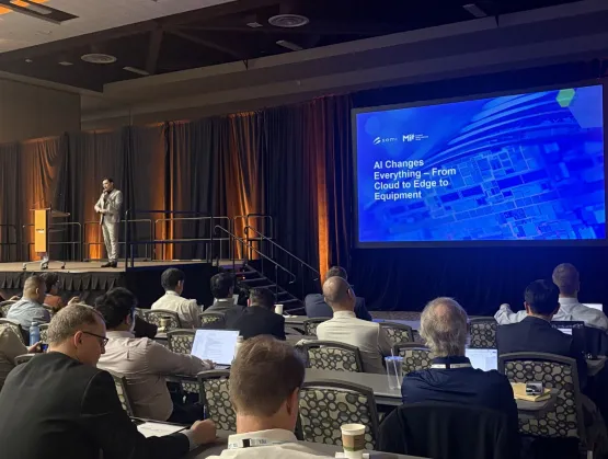
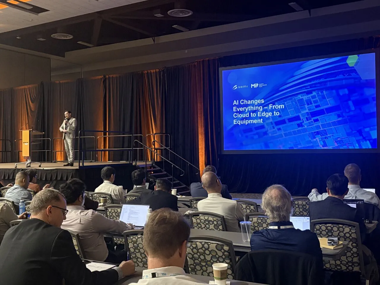
The 2025 SEMICON West Market Symposium brought together leading analysts and strategists to decode the powerful forces shaping the global semiconductor market. Building on last year’s focus on fabless growth and workforce initiatives, this year’s sessions centered on the rising influence of geopolitics, trade policy, and AI-driven investment. Experts from SEMI, Integrated Insights, Boston Consulting Group, Kearney, PwC, WSTS and TechSearch shared perspectives on how global shifts from tariffs to technology races are redefining supply chain resilience and regional competitiveness.On October 6 in Phoenix, Arizona, Clark Tseng, Senior Director of SEMI Market Intelligence, hosted the symposium and presented along with industry experts on the current trade environment from various angles. Discussions ranged from the effects of U.S. tariffs across the globe, to sector-specific considerations and market growth areas. US Trade Dynamics in Semiconductors As the geopolitical landscape in the U.S. becomes more complex, Iacob Koch-Weser, Associate Director, Global Trade Investment at Boston Consulting Group outlined the impact that tariffs are having on the U.S. industry. The average American tariff, he said, is higher than any time in the last 75 years. Although the semiconductor industry is less affected by high tariffs than other sectors, Koch-Weser noted that might change with the administration’s expanded Section 232 Tariff that imposes 50% tariffs on steel, aluminum, and their derivatives on nearly all trading partners. To explain, he described four potential Section 232 tariff scenarios, underscoring limited Section 232 enforcement as the ideal approach.Tariffs may be deprioritized in favor of chips incentivesThere may be targeted carveouts for alliesThe administration may impose high tariffs with limited exceptionsThere may be a 100% tariff rate To cope with tariff uncertainty, Koch-Weser recommended that companies consider reshaping policies, mastering trade compliance, and reconfiguring supply chains if possible. He also shared four potential outcomes for the future of U.S. trade that could take effect within the next 18-24 months. The U.S. may run its own system while the rest of the world aligns to World Trade Organization (WTO) rules.North American countries may form a stronghold, leaving all other countries to choose between the North American alliance and WTO standards.Countries may form new blocs and preferential agreements, creating multiple economic spheres worldwide.Global cooperation could break down, forcing countries to fend for themselves.With everything considered, he reinforced that the U.S. is still an attractive place for semiconductor investment. The current administration, he said, recognizes the importance of bringing advanced technologies back to the U.S. Navigating Uncertainty: AI-Driven Growth and the U.S. Semiconductor Manufacturing RenaissanceContinuing discussions on tariffs, SEMI’s Clark Tseng painted a picture of the current U.S. semiconductor industry. He divided his presentation into four key areas: near-term economic uncertainty, AI changes everything, semiconductor market equipment forecast, and material market outlook.Near-term economic uncertainty: U.S. tariff policies are contributing to inflationary pressures and altering global trade patterns, leading to cross-border uncertainty that is slowing investment. U.S. tariff revenue, he said, has expanded from $7 billion in January 2025 to $29.5 billion by August, forcing companies to sacrifice margins to compensate. AI changes everything: By 2030, Tseng noted that nearly half of the semiconductor industry’s capital expenditure will be driven by AI, pointing to sustained growth in AI-driven cloud infrastructure spending through 2028 forecasts. AI is also moving beyond data centers into edge computing and endpoint devices.Semiconductor market equipment forecast: Tseng reported that the outlook for the equipment market remains strong over the next three years. However, the biggest risk to the market is a potential slowdown in AI investment and adoption. Additionally, U.S. export controls and changes in regional supply chains present some challenges. Last year, China was the largest market for semiconductor equipment, but Tseng expects continued normalization amid broader market adjustments. Taiwan and South Korea experienced the strongest year-over-year growth, driven by demand for AI chips and high-bandwidth memory (HBM). Material market outlook: Silicon wafer shipments grew strongly in Q2 of 2025, but Tseng flagged this as unexpected and cited tariffs as a possible explanation. He noted the 300mm wafer segment is expected to grow 7% in 2025, while 200mm is projected to decline. The total wafer material market, he said, is also expected to grow by 6% this year. Additionally, wet chemicals experienced a 16% expansion in 2025, while silicon wafers, photolithography materials, and CMP materials are in recovery. Semiconductor Market – Status Outlook Tobias Pröttel (or Proettel), CEO of World Semiconductor Trade Statistics (WSTS), reported that the industry’s rebound remains firmly on track, with the latest WSTS statistics confirming a 19% year-over-year increase in global semiconductor sales during the first half of 2025. Total revenue reached $346 billion over the period, supported by strong demand for AI-driven infrastructure and next-generation data centers. Based on this solid first-half performance, WSTS has raised its full-year 2025 forecast to $728 billion, representing 15% annual growth, and now expects the market to reach around $800 billion in 2026, keeping the industry on course toward the $1 trillion milestone before the decade’s end.Logic and Memory continue to lead the expansion, driven by GPUs, AI accelerators, and high-bandwidth memory (HBM), while other product categories are showing steady recovery after the recent downturn. Pröttel noted that this growth is not confined to a single region: the Americas, China, and Asia Pacific are all posting double-digit gains, reflecting strong global momentum across the semiconductor value chain.Strategic Approaches to Semiconductors by Major Economies Following Pröttel, Kearney’s Vice President, PERLab, Sanjay Kumar outlined the semiconductor investment climates in South Korea, Japan, Taiwan, and India. South Korea is currently focused on maintaining its lead in memory, diversifying into logic, localizing its supply chain, developing advanced packaging capabilities, and investing in startups. Kumar also noted the Korean approach of offering loans, as opposed to the U.S. strategy of providing direct grants. In addition, Kumar said the Korean government plays an active role in how it wants its companies to grow, whereas the U.S. takes a more passive approach in this regard.Japan is also honing its leadership in key areas like materials and memory, and Kumar also pointed to the country’s efforts to build additional advanced packaging capacity. Japan, he said, aims to grow its industry though a mix of grants, loans, and tax credits. Among the country’s notable subsidies include a 50% subsidy for TSMC – its largest so far – as well as a $4 billion subsidy for Rapidus. Taiwan’s semiconductor industry is critical for protecting its national security. As a region with limited land, power, and water, Kumar noted that Taiwan is currently focused on developing its talent base. Its government is offering tax credits for R D and equipment and up to a 50% cost share for R D projects. India, he said, has one of the most ambitious incentive programs in the world. Through its India Semiconductor Mission (ISM), the country offers a 50% federal subsidy, in addition to a 20-30% state subsidy in its quest to cover the entire semiconductor ecosystem. Kumar also spotlighted some of India’s successes – like the joint venture between Renesas, CG Power and Industrial Solutions, and Stars Microelectronics – to build a new OSAT facility.Adapting to New Policy and Navigating the U.S. Semiconductor Landscape – Insights from Taiwan Taiwan is a critical trade partner of the U.S., ranking fourth in total trade volume as of July 2025. With Taiwan’s stronghold on the U.S. chip ecosystem, Paul Poliakov, Senior Manager, International Tax Services, CPA at PwC Taiwan detailed both the bottlenecks and developments regarding Taiwan companies’ investments in the U.S. Among the investment bottlenecks he highlighted were higher costs of building facilities in the U.S., multiple layers of compliance requirements that may be intimidating for new market entrants, and complex visa and tax regulations. In addition, Section 232 investigations on semiconductors are ongoing, with several potential policy changes that could take effect. The pending United States-Taiwan Expedited Double-Tax Relief Act could help ease burdens, he said, but it has yet to pass in the U.S. Senate as of October 2025. If it passes, it will integrate benefits for Taiwanese individuals and businesses into the U.S. tax code, which could substantially benefit Taiwanese investment in the U.S., including manufacturing, services, distribution, and a wide variety of other industries. Furthermore, Poliakov suggested that businesses maintain flexibility in their investment strategies, engage with U.S. state and local governments that can offer investment incentives, and work with professionals to ensure regulatory compliance. Geopolitical Shifts in Advanced Packaging AssemblyIn the final presentation of the 2025 Market Symposium, Jan Vardaman, Founder and President of TechSearch International provided an overview of the current advanced packaging market. Although advanced packaging represents the highest growth area in the industry, Vardaman highlighted that packaging complexity is also soaring. R D, testing, and equipment support infrastructure, she said, are becoming more critical for meeting future packaging needs. Even though assembly is mostly done in Asia, new U.S.-based advanced packaging facilities from Amkor, TSMC, and others represent signs of change. Still, Vardaman noted that the U.S. has almost no capability to produce advanced IC substrates using build-up film, which are needed to support high density applications. In addition, she highlighted that building more silicon fabs on U.S. soil won’t solve its national security or supply chain concerns.For the U.S. to create a sustainable packaging ecosystem, Vardaman concluded that support of assembly facilities is crucial. Ultimately, businesses must be willing to pay more for U.S.-based packaging in favor of potential supply chain resilience and national security benefits. SEMI would like to thank all speakers, sponsors, and attendees for the success of this year’s Market Symposium. Explore the latest SEMI Market Intelligence reports, covering historical reporting, actionable foresight into emerging trends and technology investments to make confident, forward-looking decisions across the semiconductor and microelectronics value chain.Clark Tseng is Senior Director, Market Intelligence Team at SEMI. Nishita Rao is Director, Product Marketing at SEMI.
Read More
The semiconductor industry continues to push the boundaries of innovation, making quality management more critical than ever. To address these challenges, SEMI Quality Benchmarking Consortium (QBC) brings together leading companies to share best practices, benchmark performance, and drive collective improvement across the global semiconductor ecosystem.The latest QBC meeting was hosted by Roberto Lissoni of STMicroelectronics at their Agrate site near Milan, Italy. Representatives from Bosch, GlobalFoundries, Infineon, Micron, NXP, and Texas Instruments gathered for two days of deep discussion and knowledge exchange. (From Right to Left) – Roberto Lissoni (STMicroelecetronics), Giorgio Cesana (STMicroelectronics), Fern Yoon (Texas Instruments), Jens Luepke (Infineon), Mark da Silva (SEMI), Kerstin Nocke (Bosch), John Lepper (GlobalFoundries), Bill Lechten (Micron), Lou Cerra (NXP)With over 5,000 employees, ST’s Agrate facility is the company’s largest in Italy, with a strong commitment to innovation through university collaborations. The site includes both 200mm and 300mm wafer fabs, R D centers, and product development teams. STMicroelectronics Agrate, ItalyThe QBC operates on a “Give-to-Get” philosophy: members must actively contribute survey responses and participate in open discussions to access shared benchmarking data. This meeting focused on four topics: zero defect customer satisfaction, safe launch, knowledge management, and organizational comparisons. Participants presented their approaches, shared lessons learned, and engaged in roundtable discussions to identify best-known methods and address common challenges. Zero Defect and Continuous ImprovementParticipants explored the evolving definition of “zero defect,” emphasizing that it’s not about literal perfection, but about meeting customer commitments and requirements. Quality programs are multi-year, cross-functional initiatives, often embedded in broader operational excellence campaigns. Companies leverage KPIs such as parts per million, cost of nonconformance, and customer satisfaction. They tie these metrics to incentive programs and executive reporting. Continuous improvement is driven by Lean, Six Sigma, and employee engagement, with a strong focus on early detection (“shift left”), cross-functional teams, and digital tools for analytics and feedback. Customer Satisfaction and ScorecardsCustomer scorecards and surveys are central to measuring satisfaction, with processes varying by region and account type. Most organizations use a mix of manual and automated systems to collect, review, and act on scorecard data, supplementing these with relationship and transactional surveys. AI and predictive analytics are emerging tools for anticipating customer feedback and improving proactive management, though data security remains a priority. Safe Launch and Risk ManagementThe QBC companies shared decision criteria, risk assessment methodologies (FMEA, TRA), and enhanced control plans for new products and technologies. Cross-functional collaboration is key, with product quality managers accountable for planning and reporting. Digitalization and integration with manufacturing execution systems (MES) are advancing, and there’s growing interest in leveraging AI for risk assessment and process optimization. Knowledge Management and Lessons LearnedKnowledge management remains a challenge, with most companies relying on distributed databases, expert teams, and informal networks. They are piloting structured lessons learned forums, audit systems, and semantic search tools to improve findability and reuse. Effective knowledge management happens when insights are embedded directly into business processes, supported by continuous review and governance. Looking Ahead: AI, Predictive Quality, and ExpansionThe consortium plans to explore topics such as artificial intelligence, predictive quality management, and secure data sharing through dedicated sessions and working groups, with a focus on practical applications and insights from external subject matter experts.Read about the first QBC meeting hosted by Infineon here. Sarah Shen is Senior Coordinator, MEMS Sensors Industry Group at SEMI.
Read More
Last month, leading-edge equipment company ASML announced a surprising €1.3 billion investment into French AI company Mistral. The two companies touted stronger collaboration and the desire to “innovate faster together.” Even though some observers were skeptical, the commitment of one European tech champion into an aspiring European tech firm in the world’s hottest industry made plenty of sense. Writing for Bloomberg, columnist Lionel Laurent noted that such a deal was “a win for Europe’s tech ambitions” and that Mistral would have increased credibility in an AI race dominated by the United States and China.Europe’s tech prowess indeed lags behind its global rivals. ASML is, perhaps surprisingly (or not, depending on your vantage point), Europe’s largest tech giant by market cap at $406 billion. Europe boasts no tech goliaths the size of Amazon or NVIDIA and is often left following the lead of American tech firms as they chart the commercialization of new technologies. In the semiconductor industry, Europe’s chip manufacturers comprise only 9% of global market share today compared to 44% in 1990. Despite the bleak reality that Europe’s tech ecosystem finds itself in, there are reasons to believe that the nadir of recent years is slowly giving way to a more robust and respected innovation landscape. This piece will focus specifically on semiconductor manufacturing, demonstrating how Europe is taking its technological future seriously, and how, despite the challenges that remain, ultimately Europe is poised to succeed.Three Shocks – How We Arrived At This MomentThough Europe may not have been satisfied with the technological balance of power of recent decades, such an arrangement was largely tenable in a globalized world which prioritized free markets and international security in the aftermath of the Cold War. Though numerous cracks appeared in previous decades, the last five years in particular have given way to three shocks which have awoken European policymakers.The first, of course, was the COVID pandemic and the decimation of supply chains that caused a rapid seesaw in chip inventories – from extreme shortage to extreme oversupply – that companies in the automotive and industrial sector are just now recovering from. One senior German official was quoted as saying, “We lost 1-1.5% of our GDP in 2021 because of a lack of semiconductors – or about €40 billion.”Only two years later would come Russia’s unthinkable invasion of Ukraine, an unwelcome new reality which has forced Europe to reckon with its defense posture and supply chain. Semiconductors, again, play a key role here – Europe is reliant on China’s legacy chip production, meaning that low-tech chips often find their way into strategic weaponry.Lastly, a second Trump administration has surprised and rallied European governments to respond to “America first” rhetoric. Combined with the aforementioned shocks, recent events have convinced even Europe’s most ardent globalists that the continent must now invest where necessary in order to protect its borders and foster a competitive and sovereign technology ecosystem.The Underwhelming Response So FarFast forward to today where Europe’s COVID supply chain disruptions quickly gave way to ambitious policy in the form of the €43 billion European Chips Act intended to stimulate private investment to complement public capital and push Europe’s chip manufacturing market share to 20%. In the more than two years since the legislation’s passing, however, announced projects have underwhelmed. Big splashes from Intel and Wolfspeed have failed to materialize due to overambitious market expectations. Today, you can almost count the key recipients on one hand – STMicroelectronics, Infineon, TSMC, GlobalFoundries, Silicon Box, and amsOSRAM.Despite the sense of cynicism from some corners, however, understanding the slow progress to this point helps to unlock the right strategies moving forward. Already, many industry stakeholders and policymakers have questioned if attracting manufacturing full stop is the right strategy. Peter Wennink, former CEO of ASML, called the European Commission’s target to secure 20% of the global chip market by 2030 “totally unrealistic,” emphasizing that Europe’s current share is “8% at best.”Even if Wennink’s conclusion is too harsh, the tangible lack of investment over the past couple of years paired with the urgent need for Europe to maintain and grow its semiconductor prowess in response to concerns of security and sovereignty still demands a workable solution. The answer lies in building upon Europe’s very real strengths in the chip industry, narrowing the scope of investment to key strategic areas and in continuing to prioritize collaboration at all costs. How Europe Can Still Meet The MomentAny conversation about Europe’s contributions to the global semiconductor industry should begin with its unparalleled research ecosystem, and there’s no better place to start than with Belgium’s imec, one of the foremost research institutions chip companies depend on. Earlier this year, imec’s President and CEO Luc Van den hove emphatically reminded his audience that “you can’t make an advanced chip without European technology.” Van den hove’s point was that Europe should be leaning into its strengths as a research powerhouse rather than trying to chase leading-edge nodes. The FAMES Pilot Line is one example of what that research prowess looks like in practice. Funded with €830 million via the EU Chips Act, the initiative brings together Europe’s leading research institutions (imec, Fraunhofer, CEA-Leti, and Tyndall) to develop open access to several key microelectronic technologies, with a strong emphasis on low-power applications for markets such as automotive, IoT, and mobile devices. Central to FAMES is its “open access” policy which enables European manufacturers to use its pilot line to develop prototypes and evaluate next-generation technologies. Chip companies without any manufacturing presence in Europe stand on the outside looking in, risking technological inferiority.While Europe flexes its academic prowess, however, it is increasingly recognizing its vulnerability when it comes to more mature-node technologies and production. Investments such as ESMC – TSMC’s joint-venture with regional champions Bosch, Infineon, and NXP – are a good start, but Europe fundamentally needs more mature tech, particularly for defense. In a recent piece for Foreign Affairs Magazine, authors Chris Miller and John Allen argued that Europe indeed has a promising semiconductor opportunity ahead of it, but only if it enhances cooperation with the United States. The fact that the two regions have similar goals and geopolitical rivals is an opportunity for Europe to attract greater chip investment from U.S. firms looking for Europe’s leading research capabilities and defense customers. The authors implore European policymakers to:“ensure that their chip companies can capitalize on the surge in defense spending by investing more in new defense technologies and fostering connections between large chip firms and small defense start-ups. European chip companies that have previously focused on civilian markets must realize that the defense industry, and particularly the drone sector, will drive growth and technological change.”Targeting these investments intelligently remains to be seen, but there can be no doubt that Europe is taking the funding challenge seriously. Germany, France, Italy, and the United Kingdom have all raised their defense spending as a percentage of national income, with Germany announcing plans to double its defense spending to €650 billion over the next five years.Securing Position In Europe's Semiconductor RenaissanceEurope’s semiconductor future will not be built by mimicking Taiwan’s fabrication prowess or outspending America’s subsidies. Instead, success lies in doubling down on what Europe already does exceptionally well – world-class research infrastructure, strategic positioning in mature and specialty nodes, and an increasingly robust defense industrial base hungry for secure semiconductor supply. As European chip subsidies continue and defense budgets surge across the continent and geopolitical fractures deepen, the strategic calculus is clear – semiconductor companies without meaningful European capacity risk ceding ground to competitors who recognized the shift early. The question is no longer whether Europe matters in the global chip ecosystem, but rather which companies will position themselves to capitalize on its inevitable growth.About Stephen M. RothrockStephen Rothrock founded ATREG in 2000 to help the world’s advanced technology companies divest and acquire infrastructure-rich manufacturing assets, including wafer fabs (front- and back-end) as well as MEMS, solar, display, and R D facilities. Over the last 25 years, his firm has completed 40% of all global operational wafer fab sales in the semiconductor industry, a total of 60 transactions. Recent global acquisitions and dispositions have involved Allegro MicroSystems, Bosch, Elmos, Fujitsu, GlobalFoundries, IBM, Infineon, Japan Display (JDI), Micron, NXP, onsemi, Qualcomm, Renesas, Sony, Texas Instruments, and VIS to name just a few. Prior to founding ATREG, Rothrock established Colliers International’s Global Corporate Services initiative and headed the company’s U.S. division based in Seattle, WashBefore that, he worked as Director for Savills International real estate brokerage in London UK, establishing their global corporate services platform serving large multinationals, many of whom were leading technology companies. Rothrock also served on the UK-listed property company’s international board. He spent four years near Paris, France working for an international NGO. Rothrock holds an MA degree from the University of Hull, UK and a BA degree in Business Commerce from the University of Washington in Seattle, USA.
Read More
Maheen Hamid is a co-founder of Breker Verification Systems, supplier of functional verification solutions for complex chip design challenges, and serves as its COO and CFO. She is also Co-Chair of the ESD Alliance and member of the SEMI North America Advisory Board (NAAB).Given her background, roles within the industry and interests, it seemed like a good time for me to reach out for her perspective and market analysis. During our discussion, she offered up some great observations, identified trends, pointed to areas in need of attention and ways for the industry to better collaborate. We ended by talking about AI’s role today.Smith: How do you track where the semiconductor industry is going?Hamid: Business and macro strategies have always been interesting to me. In recent years, with the increasing global importance of silicon sovereignty, it is necessary to track the pulse of initiatives across various channels in multiple geographies. Starting with policy discussions at SEMI to media coverage of the semiconductor value chain to EDA specific news, I read voraciously and listen in on disparate discussions. There is no denying that it is impossible to envision the boundaries of where the semiconductor industry could go, particularly in design innovation. Smith: Nonetheless, what trends have you identified?Hamid: Global trade wars are creating as many roadblocks as they are creating opportunities. It is fascinating to watch the incredible innovation led by the U.S. for decades in semiconductor design be challenged as technology and access to technology gets democratized across the board. Maintaining thought leadership is a demanding task and no longer contained to an individual company’s cleverness. Crafting an effort that is coordinated with national interests has become compulsory. Separately, developments in AI are creating a new wave of complex chip designs that are redefining hardware investments. Data centers are becoming as ubiquitous as the personal computers of the ‘80s. While advanced chip designs forge ahead and additional classes of chips such as memory become truly commoditized, the need for efficiency in the full flow from design to manufacturing becomes imperative to protect margins for relevant players.Smith: The need for industry collaboration appears to be a trend that is an essential part of the industry’s evolution. How do you see that developing in chip verification?Hamid: RISC-V has given rise to many new design starts by companies that do not have the legacy verification frameworks owned by the NVIDIAs and Intels of the world. Several of these larger customer companies are investing heavily in their own complex chip designs, creating interesting opportunities for a collaborative approach to enabling internal innovations. As well, this new class of customers is less married to enterprise flows from large EDA companies and prefer to invest in best-of-breed solutions. This is driving necessary collaborations across EDA vendors in chip verification. Driven by mutual customer demand, we have recently modified several of our arrangements with other EDA players.Interestingly, the momentum in the RISC-V ecosystem is also driving new initiatives in the more traditional flows. This is a necessary shake-up in how business needs to be done in an increasingly, globally competitive landscape. Smith: What area do you see that needs more attention?Hamid: It is imperative to keep the business climate conducive for innovation and thought leadership. Policy debates impacting the chip industry are getting more heated and controversial. We need more concerted collaboration among the players in the chip ecosystem to help influence this policy in a way that allows U.S. companies to thrive. We need to promote more opportunities that bring disparate companies together to build clever flows that increase our silicon sovereignty. Smith: AI is playing in the design and design tools area. What about other parts of an organization, such as finance or operations and marketing?Hamid: AI efficiencies can help with predictive analysis for large companies in these core functions such as finance, operations and marketing, but for smaller, nimble companies, the human element still rules. Our strategic marketing, as an example, is defining industry-leading initiatives. AI does not have access to language models to automate any of what we need to invent in communicating new ideas. LLMs do provide a good sounding board though. It’s interesting to “discuss” ideas with ChatGPT and pull templates of successful implementations in unrelated industries that could be a blueprint for how we approach next steps.About Maheen HamidMaheen Hamid is the co-founder CFO and COO at Breker Verification Systems, bringing a wealth of financial engineering experience from investment banking and small business management. Hamid has been instrumental in establishing Breker as an important stakeholder in the EDA industry, running its business side and driving operational growth as it thrives as an established software supplier. She plays an active role in defining the company’s strategic direction, corporate communications and branding. Hamid holds a BBA from North South University and an MBA from the University of Texas at Austin.Robert (Bob) Smith is executive director of the ESD Alliance, a SEMI Technology Community. 
Read More
The New Reality of Semiconductor Supply ChainsThe semiconductor industry is one of the most globally connected and time-sensitive sectors in existence. From design and wafer fabrication to testing, assembly, and delivery, every step depends on flawless coordination across borders, suppliers, and time zones. More than 1 trillion chips move through global supply chains each year[1], connecting suppliers, foundries, and fabs across continents.But as the world becomes more complex and unpredictable – with trade tensions, capacity shortages, shifting technology cycles, and driven by increasing AI and energy demand – that coordination is increasingly under pressure. Even a minor delay in one place can halt production in another. A single missed component, delayed shipment, or grounded flight can trigger line-down costs that can exceed $4 million per hour in advanced fabs[2].That’s why logistics is no longer a background process; it’s a strategic function that directly influences performance, reputation, and profitability.Figure 1 - We live in a complex and unpredictable world where global events have significant impacts. When Every Hour MattersFew industries feel the impact of delays as directly as semiconductors. One missing component, a grounded flight, or a customs delay can trigger a chain reaction that stops production lines, delays product launches or breaks contractual commitments.Time-critical logistics plays a distinct role in safeguarding supply chain performance, staying in control and enabling companies to recover in hours instead of days. It serves as the system’s shock absorbers when conventional routes are disrupted, timelines collapse, or customer commitments are at risk.The ROI of UrgencyTime-critical shipments are costly—but in the semiconductor world, not acting fast is far more expensive and pose significant consequences. A single line-down event can cost millions of euros per day, depending on the process stage and the customer involved. Compared to that, the premium for a same-day or next-flight shipment is minimal.When companies integrate time-critical logistics as a planned capability, the ROI becomes tangible.Avoided downtime: Faster recovery after supply interruptions directly protects production yield and customer commitments.Reduced inventory buffers: If rapid response capacity is available, less working capital is tied up in safety stock.Customer retention: Reliable continuity strengthens trust and long-term business relationships.In this sense, time-critical logistics isn’t just an operational expense – it’s a continuity investment. It protects revenue streams and reputation and gives manufacturers the agility to respond to whatever the next disruption brings.Example scenarios include:A single fab tool delay can idle an entire production line, costing millions per hour. During the 2024 Taiwan earthquake, a single supplier delay triggered hundreds of millions in global production losses.A next-flight-out or onboard courier shipment typically represents less than 1% of that downtime cost.Rapid recovery also prevents ripple effects such as delayed customer deliveries.The companies that embed time-critical logistics as a strategic capability gain not only cost protection, but competitive agility.From Efficiency to AgilityTraditional supply chains were built for stability and scale: move high volumes, keep costs low, and plan far ahead. But in the semiconductor industry, speed and adaptability now define competitiveness.Agility means having the systems, partners, and mindset in place to act decisively when the unexpected happens. Leading companies are now integrating dedicated control towers, predictive data insights, and predefined emergency logistics playbooks – turning reaction time into a measurable performance indicator. However, agility is not only a matter of infrastructure – it depends on data-driven visibility and cross-industry collaboration.Collaboration as the Real DifferentiatorNo company can face disruption alone. Semiconductor supply chains depend on the combined coordination of equipment makers, material suppliers, foundries, logistics providers, and government agencies.Collaboration is therefore the new competitive edge. Shared standards, visibility tools, and coordinated crisis response frameworks – like those developed under the SEMI Supply Chain Management Initiative – are helping the industry build collective resilience. These cross-functional efforts are where innovation scales.Looking AheadThe semiconductor industry will continue to expand into new regions and technologies. Each step adds complexity and, with it, vulnerability. The next decade will test not just how fast companies can produce, but how fast they can recover. Future disruptions – whether geopolitical, environmental, or digital – are inevitable. The question is not how to avoid them, but how to respond faster and smarter when they occur.That’s where time-critical logistics will continue to make its mark. It is more than just a transport solution. It gives companies the ability to act decisively in moments that matter most – transforming time from a constraint into a competitive advantage that ensures business continuity.Key TakeawaysSemiconductor supply chains are uniquely time-sensitive — a single delay can halt multimillion-dollar production lines.Integrating time-critical logistics improves responsiveness, reduces inventory needs, and safeguards business continuity.Agility, not efficiency, will define the next decade of semiconductor competitiveness.Collaborative industry frameworks like the SEMI Supply Chain Management Initiative are key to building resilience.How ready is your supply chain?Learn more about time:matters’ tailored logistics solutions at SEMICON Europa 2025 (Hall C2, Booth 433), November 18-21 in Munich and attend the company’s presentation on the TechARENA stage on November 19. For more information or to schedule a meeting at SEMICON Europa, click here to contact Remy Schoenzetter.Remy Schoenzetter is Global Head of Business Unit High Tech Semicon at time:matters.[1] Statista: Global semiconductor unit shipments 2021; SIA/WSTS Annual Reports[2] McKinsey: "Need to boost semiconductor fab efficiency?" (2023); LinkedIn Air Monitor analysis (2025); Critical Manufacturing Industry Blog (2024)
Read More
The semiconductor and electronics industries are at a turning point. Once defined by efficiency and scale, supply chains now face a convergence of pressures—from geopolitical tensions and climate risks to accelerating innovation cycles. The stakes are higher than ever, but so are the opportunities to reimagine how this global ecosystem operates.The End of “Just-in-Time” as We Knew ItIn 2025, one thing is clear: the old “just-in-time, globally concentrated” supply chain model can no longer carry the industry forward. Trade policies are tightening, export controls are multiplying, and tariff investigations are fragmenting markets that once felt seamlessly connected.At the same time, natural resource risks are mounting. PwC estimates that by 2035, nearly one-third of global semiconductor production could face copper supply disruptions caused by climate change. That figure rises to nearly 60% by 2050 if emissions remain unchecked. Add to this the growing maze of regulatory barriers and import restrictions on raw materials, and the industry faces rising procurement challenges and relentless cost volatility.Demand Isn’t WaitingWhile supply chains struggle with constraints, demand continues its upward climb. Global chip sales are rebounding, driven by innovation cycles in AI, automotive electronics, 5G, and renewable energy. Bringing new manufacturing capacity online takes years. The imbalance is widening, and companies can’t afford to rely on outdated, reactive supply chain models.Resiliency has become mission critical. And as the saying goes: you can’t respond to risks you can’t see. Guesswork isn’t a strategy—especially when disruptions are systemic.Fragility in a Fragmented EcosystemSemiconductor production is specialized and geographically fragmented. A disruption at a single node—whether a mine, a fab, or a logistics hub—can ripple through the ecosystem in days or even hours.Recent shocks have only reinforced this fragility:Trade restrictions are pushing manufacturers to rethink supply chain design.Climate change is endangering raw materials like copper and quartz, both highly water- and energy-intensive to produce.Market volatility is being driven by the explosive rise of AI and data center demand.The lesson is simple: resilience is no longer optional—it’s an existential requirement. And the path to resilience runs through visibility, agility, and collective intelligence.Real-Time Intelligence: From Luxury to NecessityIn today’s environment, quarterly or even monthly reporting cycles are dangerously slow. By the time a shortage, tariff, or logistics reroute appears on the radar, the window to act may have already closed. The cost of waiting—or doing nothing—is steep, and the damage can be lasting.Real-time data and AI-driven insights aren’t “nice-to-have” tools anymore. They are strategic imperatives for supply chains under constant stress. They allow companies to anticipate risks, respond faster, and align more effectively with partners across the ecosystem.Collaboration Is the New CurrencyNo company can go it alone. A chipmaker depends on its suppliers, just as a rare earth miner depends on transport partners. The global supply chain is a living system—and its resilience depends on the strength of its interconnections.Deeper supplier relationships, visibility into Tier 2 and Tier 3 suppliers, and shared intelligence on geopolitical and regulatory shifts are all critical. Resiliency isn’t built in silos; it’s forged through collective action.Building the Future TogetherThe semiconductor and electronics industries stand at the threshold of a new era—one of collective risk but also shared potential. Companies that embrace transparency, real-time intelligence, and collaboration will not just survive shocks, but emerge stronger, more agile, and better prepared to lead.In this new chapter, collaboration is the currency of resilience.That’s where Conductor™ comes in: a real-time intelligence platform built to help industry players anticipate, adapt, and act – together. Conductor weaves all those threads together, delivering not just data, but a shared situational awareness, helping the industry to think and act as a system rather than a collection of silos.What Conductor Enables - and What It Could Lead ToSmarter, faster decisionsA platform like Conductor, which uses near real time data, AI-powered news and alerts, and community-driven insights, turns reactive “damage control” into proactive “risk management.”By bringing together cross-segment, critical KPIs, curated AI news, expert analysis, and peer-community intelligence, Conductor helps teams understand what’s happening now, assess the likely impact on their business, and decide how to respond - faster, and with more context.Over time, this could shift the default mode of the industry from “fire-fighting” to “anticipatory steering.”A more adaptive supply chainAs more organizations adopt the platform, the collective visibility improves. Conductor can power scenario planning, enable early warning systems, and foster agile “micro-pivot” strategies: reroute logistics, adapt sourcing, or reallocate production before a disruption becomes a crisis.New models of ecosystem resilienceWith consistent, shared intelligence, industry players can identify common vulnerabilities and coordinate mitigation for mutual gain. Over time, this could lead to more resilient operations through diversified sourcing strategies, and even shared contingency mechanisms.In short: Conductor is a building block toward a more distributed, more transparent, more resilient global semiconductor ecosystem.Accelerated innovation cyclesWhen the risk of disruption is better managed, companies can operate with more confidence, investing in new capacity, experimenting with new chip architectures, or integrating new markets more aggressively. Technology diffusion accelerates when the fear of “what-if” is reduced.Where We Go From HereConductor is already in early-access pilot phase, and feedback from the SEMI Supply Chain Management Initiative’s Industry Advisory Council is actively shaping its evolution.As adoption spreads, network effects will increase the platform’s predictive power, making it more valuable for everyone involved.In an industry that’s increasingly defined by fast change and high stakes, tools like Conductor shift the balance: from reactive scramble to informed strategy, opaque fragility to visible resilience, and from isolated action to ecosystem collaboration.The future of supply chain resilience starts here. Sign up for early access to Conductor today and help drive the new era of trade.Talal Abu-Issa is Co-CEO and Co-Founder of Beebolt.Krish Dharma is Strategic Advisor, SEMI Supply Chain Initiative.
Read More
Political leaders worldwide are investing hundreds of billions to reduce semiconductor dependencies and secure their positions in this nearly $630 billion market, according to the World Semiconductor Trade Statistics (WSTS). Yet the extreme specialization and geographic concentration of the semiconductor supply chain makes complete self-sufficiency economically impractical and strategically questionable.After decades building an intricate global production network optimized for cost and innovation, the industry now faces pressure to splinter into regional blocks. But this raises important questions: Can any nation truly achieve chip self-sufficiency? And would disconnecting from the global ecosystem ultimately hurt competitiveness more than help security?The Independence IllusionThe global semiconductor industry has carved itself into specialized kingdoms. The United States dominates chip design and certain equipment categories, representing about 50% of global revenue. Taiwan controls roughly 67% of global foundry capacity through TSMC—so much so that semiconductors represent one-sixth of Taiwan's total GDP. Europe's strength lies in ASML's advanced EUV lithography technologies, the machines everyone needs but only one company currently makes.China plays an interesting double role too: it's both the largest semiconductor consumer at 50% of the global market and an important producer, holding 31% of total global foundry capacity in 2023.So far, every "independence" initiative has deepened interdependence. The US needs the Netherlands for lithography equipment. Europe needs Asia for high-end chip production. China develops much of its own equipment but remains dependent in key areas. The House of Cards ProblemFor decades, the semiconductor industry perfected making incredibly complex products cheaper every year through extreme specialization. Each company focused on one slice of the supply chain and became world-class at it. But nobody talked about what we built: a house of cards. The entire global economy now depends on a supply chain so specialized that losing even one supplier can shut down entire industries.The COVID pandemic exposed what industry insiders had warned about for years: the chip supply chain works brilliantly until it doesn't. When it fails, it fails spectacularly. The automotive industry alone lost $210 billion in 2021, and some manufacturers still haven't fully recovered.This 2021 chip shortage wasn't just a pandemic problem. Currently, rising geopolitical tensions are changing a supply crisis into a strategic nightmare, forcing countries to rethink their entire approach to semiconductors and their production.The Barriers to IndependenceThe semiconductor industry faces serious barriers that make true independence incredibly difficult for any single nation.First, the supply chain depends on chokepoints controlled by just a few companies in specific regions. Electronic Design Automation tools—essential software for designing any chip—come mostly from three US companies: Synopsys (~31%), Cadence Design Systems (~30%), and Siemens EDA (~13%). Without these design tools, you simply cannot create modern semiconductors. Manufacturing equipment presents an even tighter bottleneck, with ASML holding 100% control of EUV lithography machines needed for advanced chips. Second, the talent shortage makes building new capabilities nearly impossible. By 2030, semiconductor companies will need 1 million additional skilled workers. Developing semiconductor expertise takes a decade of hands-on experience, and most skilled professionals already work in established industry clusters like Taiwan, South Korea, and Silicon Valley. You can't simply relocate these engineers or train new ones quickly enough to staff multiple new regional semiconductor industries.Third and finally, resource requirements exceed what most countries can realistically provide. Building advanced semiconductor chip plants costs $20-30 billion each and they take years to construct before producing a single chip. These facilities consume up to 15 million litres of ultra-pure water daily and large facilities require up to 100 megawatt-hours of power per hour. Beyond the physical infrastructure, technical complexity has made first-time silicon success rates drop to just 14%, while 40% of semiconductor demand still comes from older process nodes, requiring completely separate supply chains for different chip generations.The Trillion-Dollar Investment RaceConcerns about supply chain security have triggered government interventions worldwide. The United States committed $52.7 billion through the CHIPS Act plus additional tax credits. While President Trump initially called for eliminating the program in March 2025, he instead signed an executive order on March 31, 2025, creating the "United States Investment Accelerator" to take over CHIPS Act implementation. TSMC also announced a new $100 billion investment to build five additional chip facilities in the US.Countries across the globe are racing to establish or strengthen their semiconductor capabilities. India has entered the semiconductor competition with its $10 billion Semiconductor Mission and secured investment from Micron Technology, which is constructing a $2.75 billion assembly and test facility. Japan has intensified its semiconductor strategy by establishing Rapidus Corporation with a government support package that is estimated to reach $11.46 billion aimed at revitalizing its domestic chip industry. Meanwhile, the European Union has established a €43 billion Chips Act through 2030, China launched its third "Big Fund" phase in May 2024 with $47.5 billion, and South Korea has developed a $450 billion K-Semiconductor strategy through 2030.These initiatives are changing the semiconductor industry on a global scale. However, complete self-sufficiency would require significant additional global investment and result in 35-65% semiconductor price increases due to suboptimal scale and inefficiencies.What Comes NextThe quest for chip self-sufficiency has become a trillion-dollar global endeavor, with countries placing enormous bets on facilities that may not pay off for years. Complete semiconductor independence remains financially prohibitive for any country, but strategic resilience is achievable.The winners will be those who build the most resilient networks and manage interdependence best. Rather than chasing impossible independence, nations should focus on strengthening their existing advantages while addressing their most vulnerable dependencies. Full independence remains a fantasy, but smart interdependence offers a realistic approach to semiconductor security.Click here to read the full white paper.About the AuthorsJan-Bart Smits is a Managing Partner at Stanton Chase Amsterdam. He began his career in executive search in 1990. At Stanton Chase, he has held several leadership roles, including Chair of the Board, Global Sector Leader for Technology, and Global Sector Leader for Professional Services. He currently serves as Stanton Chase’s Global Subsector Leader for the Semiconductor industry. He holds an M.Sc. in Astrophysics from Leiden University in the Netherlands. David Harap is a Managing Director at Stanton Chase Austin, bringing over 25 years of executive search experience to his role. He has successfully placed hundreds of senior executives and functional leaders across various industries. A Cornell University graduate and Father Kelly Scholar, Harap lectures at the University of Texas at Austin. He is a certified Ambassador for Hofstede Insights, bringing unique insights on organizational culture to his work.
Read More