downloadGroupGroupnoun_press release_995423_000000 copyGroupnoun_Feed_96767_000000Group 19noun_pictures_1817522_000000Member company iconResource item iconStore item iconGroup 19Group 19noun_Photo_2085192_000000 Copynoun_presentation_2096081_000000Group 19Group Copy 7noun_webinar_692730_000000Path
주요 콘텐츠로 건너뛰기
Default Banner Image

대면 행사

등록안내

Registration

사전등록은 5월 24일(금) 오후 5시에 마감됩니다.

[사전등록]

· SEMI 회원사: 308,000원
· 비회원사: 363,000원


[현장등록]

· SEMI 회원사: 385,000원
· 비회원사: 385,000원


※ 본 등록비에는 중식 및 리셉션 참가비용이 포함되어 있습니다.

Registration
대한민국 SMC Korea 2025 바로가기 SMC-Korea-2024-Banners-squre.jpg 비즈니스 기술

OVERVIEW

  • 날짜: 2024년 5월 29일(수)
  • 시간: 10:00 - 18:30
  • 장소: 수원컨벤션센터 3층 컨벤션홀 2


NOTICE

  • 아젠다는 연사 사정에 의하여 임의로 변경될 수 있습니다.
  • 행사 종료 후 참석자들에게 연사 동의를 얻은 자료에 한하여 발표자료를 공유드릴 예정입니다.


SPONSORS

SMC-Korea-2023-Sponsor_DW.jpg SMC-Korea-2023-Sponsor_DP.jpg SMC-Korea-2023-Sponsor_JSR.jpg SMC-Korea-2023-Sponsor_ET.jpg
SMC-Korea-2023-Sponsor_DS_0.jpg Air LiquideHuntsman
 
line_2.jpg


CONTACT

대한민국
경기도 수원시
수원컨벤션센터 3층 컨벤션홀 2

10:00 am - 10:05 am
 Hyun-Dae (H. D.) Cho - President, SEMI Korea
HD Cho
President
SEMI Korea

Welcome

10:05 am - 10:35 am
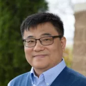
seongtae oh
오성태
펠로우
TEL

Process Technologies for Continuous Scaling of Logic Devices

The rapid growth of AI, big data, IoT, and 5/6G communication necessitates the sophisticated computing power and efficiency of semiconductor devices, driving demand for various components such as HPC, GPU, ASIC, FPGA, and HBM. Semiconductor device and equipment industries are also challenging various new technologies to accommodate such diversifying applications and proceed with sustainable development in the era of AI and ICT.
According to the roadmap over the next 10 years, semiconductor technologies are expected to develop into the scaling technologies to further extend the existing Moore's Law and hybrid device technologies that integrate legacy nodes and advanced nodes into one. Therefore, in this presentation, we will look at the latest logic technology roadmap and introduce new process technologies to implement it.
※ 연사정보

10:35 am - 11:00 am
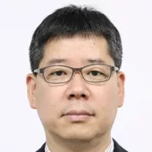
Wonho Yeon
연원호
Research Fellow
KIEP

US-China Strategic Competition and Semiconductor Export Controls

11:00 am - 11:25 am
Mark Thirsk
Mark Thirsk
Managing Partner
Linx Consulting

Localization Challenges of the Materials Supply Chain

11:25 am - 11:50 pm
Stefan CHITORAGA
Stefan CHITORAGA
Technology and Market Analyst- Packaging & Assembly
Yole Group

Material Trends in Advanced Packaging & Power Module Packaging (video recording)

11:50 pm - 1:00 pm

Lunch

1:00 pm - 1:25 pm
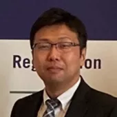
Dr. Montray C. Leavy
Montray C. Leavy
Deputy CTO
Entegris

Materials Innovation Advancing the Angstrom Era

Materials innovation within the Semiconductor industry has been a driving force since the planar 2D MOSFET to the current 3D gate-all-around (GAA) transistor architectures and will continue its criticality as we embark on 500-layer flash memory designs and Angstrom level critical interconnect dimensions. To achieve these once incomprehensible levels of lateral and vertical scaling, device design engineers and manufacturers are increasingly relying on disruptive materials innovation to enable the density and performance gains required at each successive technology node. As the performance requirements for the most advanced devices become more challenging, materials have shown to have an increased contribution to device performance over scaling and design. This has led to a greater portion of the periodic table being incorporated into semiconductor processing.

The integration of new materials, such as novel photoresists, interconnect metals & alloys, ultra-pure polymers, chemically modified polymer membranes, and formulated chemicals, into the chip fabrication increases process complexity and makes yield ramps more challenging. With more process steps in the overall device build, speed to yield and process integrity are more critical than ever to achieve technology qualification schedules. This presentation will focus on Entegris’ approach to materials innovation, the integration of these novel materials coupled with co-optimized solutions enabling industry technology roadmaps and yield requirements while preserving integrity of delivery and process control.
※ 연사정보

1:25 pm - 1:50 pm
Sadaaki Katoh
Sadaaki Katoh
JOINT2 Team Manager
Resonac

Advanced Packaging Materials and Evaluation Platform at Resonac

Resonac has started Packaging Solution Center as new R&D center to propose one-stop solution for customers in 2018 and established the co-creative packaging evaluation platform “JOINT2” with leading companies to accelerate the development of advanced materials, equipment and substrates for 2.xD and 3D package in October, 2021.

2.xD and 3D packages require to connect chips and components in high density, therefore, both wiring pitch and vertical interconnect dimension must be finer and finer. At the same time, in order to achieve better performance, more and more chips are integrated together and thus the package size is increasing. To meet these requirement, we are developing fine vertical/lateral interconnect technology and the study of fabrication and reliability for the extremely large 2.5D advanced package.

The presentation will cover the significance and strengths of JOINT2, and updates on research and development.

※ 연사정보

1:50 pm - 2:15 pm
seonjun heo.png
허성준
Process Engineering Director
Lam Research

Dry Resist for Holistic EUV Patterning

EUV lithography infrastructure has become the critical element of semiconductor industry to enable the device scaling down. It consists of not only light source, optical system but also masks, photoresist. The EUV stochastic effects present challenges to optimizing EUV resist resolution, line edge roughness, and sensitivity simultaneously. To overcome these challenges, Lam introduced the new dry resist combined with the new dry development technology.

Lam’s EUV dry resist, coupled with ASML’s EUV scanners and Lam’s holistic patterning solutions, will extend the patterning roadmap (Moore’s Law) for the next 10 years and beyond by offering a high-resolution, high-fidelity, defectivity-free, and greener solution for ≤32nm pitch L/S, and ≤40nm pitch pillar and contact hole EUV patterning in the fab. EUV dry resist technology also has been validated demonstrating superior dose-to-defectivity for <32nm pitch L/S, well suited for logic applications. Lam’s EUV dry resist is uniquely suited for future HiNA EUV patterning thanks to robust resist thickness scaling while maintaining high etch selectivity and high contrast.

※ 연사정보

2:15 pm - 2:30 pm

Break

2:30 pm - 2:55 pm
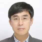
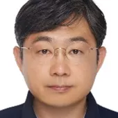
김용성
김용성
팀장
SK hynix

Sustainability Challenges of the Semiconductor Industry

As demand for chips surge, the semiconductor industry is struggling to reduce its environmental footprint. While the environmental impacts of semiconductor (and electronic products that depend on them) have mostly been liked to ‘manufacturing’ and ‘use’ phases of products which consume a significant amount of water and energy, the attention is shifting to the 'material extraction’ and ‘end-of-use’ phases of products following concerns over the e-waste issue. In this presentation, I will focus on the latest findings of the global e-waste challenge, what this means from the materials perspective, and its implications to product design and manufacturing. I will also introduce SK hynix's strategy and targets towards improving the circularity of products, and our partnership with customers/vendors to achieve a common goal.
2:55 pm - 3:20 pm
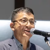
Eun-Ho Sohn
손은호
센터장
KRICT

Trends in Regulation of PFASs (per- and polyfluoroalkyl substances) and Technological Development Strategies

Fluorine compounds exhibit exceptional physical properties that set them apart from other organic materials. Consequently, they have been utilized as core materials to enhance the functionality, performance, and value of products across various key industries including electrical and electronics, semiconductors, displays, and automobiles.
However, on March 22nd of last year, the European Chemicals Agency (ECHA) issued a report imposing restrictions on the usage of over 10,000 types of per- and polyfluoroalkyl substances (PFASs) across all industries, sparking significant upheaval within the sector.
In this presentation, we will learn in detail about the definition of PFAS, and the content, progress, and schedule of PFAS regulations in Europe and the United States, and contemplate the direction of future technology development.
※ 연사정보

3:20 pm - 3:45 pm
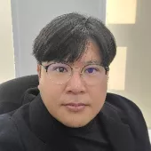
김광섭
김광섭
APAC Semiconductor Marketing Manager
Syensqo

Sustainability Opportunities for A Diverse and Secure Fluorinated Material Supply Chain

As semiconductors become more advanced and the fabrication processing conditions more extreme, the essentiality of a sustainable and secure fluorinated material supply chain plays a vital role in the future of semiconductor manufacturing. The principles of developing this supply chain are directly aligned to support the sustainability and emission roadmaps of the semiconductor industry. Syensqo will introduce the following content:
1) Priorities when Specifying Materials for a Sustainable Supply Chain
2) The Key to Sustainability - Application Segmentation
3) Case Studies
※ 연사정보

3:45 pm - 4:10 pm
dupont_Jae Hwan Sim
심재환
R&D manager/Korea R&D EUV team leader
DuPont

Innovating Safe and Sustainable by Design: Strategies and Steps toward Reduction of Substances of Concern in Photolithography Materials

Growing scientific evidences suggest that certain per- and polyfluoroalkyl substances (PFAS) pose global environmental and health risks. In response, global governments are contemplating measures to limit the use of these chemicals in various industries. However, specific types of PFAS are indispensable and no substitutes are currently available for most chip manufacturing applications in the semiconductor industry. Aligned with the objective of Safer and Sustainable by Design, DuPont has launched a comprehensive program to reduce PFAS usage in photoresist and associated lithography materials. In this presentation, we will provide an overview of DuPont's innovative initiatives and technical challenges encountered in this endeavor.

※ 연사정보

4:10 pm - 4:35 pm
Floris Buijzen
Floris Buijzen
Senior Director Product Management
Corbion

CORBION: PURASOLV® ELECT for a more Sustainable Semiconductor Manufacturing

Solvents are used extensively in the semiconductor manufacturing process. Solvents are estimated to be responsible for around 7% of the Scope 3 emissions of the semiconductor industry. The typical solvents that are used are produced from fossil resources and with that not in line with net zero ambitions. For more than 20 years Corbion has been supplying biobased ethyl lactate to the semiconductor industry under it’s brand name PURASOLV® ELECT, meeting the stringent requirements of the industry. Typical applications are photoresist for i/g-line / KrF / ArF / EUV, RRC, Edge bead removal and as thinner. Biobased ethyl lactate is sustainable and safe by design: it is produced from renewable resources, non-toxic and safe to workers, biodegradable and offers a significant carbon footprint reduction compared to incumbent solvents. Switching to biobased ethyl lactate thus enables more sustainable semiconductor manufacturing.

※ 연사정보

4:35 pm - 4:50 pm

Break

4:50 pm - 5:20 pm
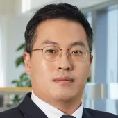
ki ill moon
문기일
부사장
SK hynix

Technology and Future of Semiconductor Packaging Materials

The technological advancement of semiconductor materials is a key factor along with the technological advancement of the process. And recently, the importance of Advanced PKG is increasing, and SK Hynix has achieved the result of improving product performance by developing MR-MUF materials. This proves the importance of materials. In the future, there are more packaging challenges for high-speed memory products such as HBM, and I plan to announce Need for material development to satisfy them.
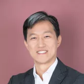
※ 연사정보

5:20 pm - 5:50 pm
Seongjun Park
박성준
팀장/Executive Vice President and Head of Material Development Team
Samsung Electronics

Big Challenges for Small Worlds

The number of transistors in semiconductor chip has been increased twice every two years for more than 50 years, following the famous Moore’s Law and somehow, it was taken to be granted. In reality, it was a big accomplishment with an unimaginable amount of efforts and collaborations, including the development of new materials.

New material has been developed and introduced to improve the performance and capacity of electronic devices through smaller design rules. New Photo Resists (PR) for higher resolution with smaller defects and higher uniformity were developed. And Precursors were also developed to meet the process challenges for the smaller design rules, such as higher aspect ratios. High etch selective Etchant and CMP Slurry with low scratch were requested. And the requirements in new materials are getting tougher and stronger with the evolution of AI, which needs more computing power than ever. Even materials that has never been expected in industry and has been studied only in academia are being actively considered.

Even the worse, the surrounding situation for material development and manufacturing is getting tougher. Environmental regulations are getting tighter. Gases with high global warming potential were begun to be replaced. Recently, EU announced banning PFAS materials in near future and US raised bars for PFAS materials. And carbon zero policy is coming to us slowly but firmly.

In this talk, we will discuss the current status and future direction of material research. We will discuss the development directions to improve the performance of devices and to consider environmental regulations. And we will discuss the virtue of working together as a big one-team to overcome all the obstacles mentioned above in the world of extreme technology.

※ 연사정보

5:50 pm - 6:30 pm

Networking Reception

EMS

Materials Resilience: Navigating Challenges, Embracing Opportunities

현재 반도체 산업은 글로벌 공급망의 안정성과 효율성이 더욱 중요시되고 있습니다. 글로벌 정치적 긴장 상황이 반도체 시장에 영향을 미치고 있으며, 이로 인해 공급망의 취약성이 더욱 드러나는 중입니다. 이에 더해, 지속적인 환경 규제 역시 산업에 미치는 영향이 점점 더 증가하고 있습니다. 친환경 제품과 생산 과정에 대한 요구가 높아지면서 기업들은 이러한 규제 준수와 함께 혁신적인 기술과 솔루션을 도입해야 하는 압박을 받고 있습니다.
이러한 동향들은 반도체 산업에 새로운 도전과 기회를 제시하고 있습니다. SMC Korea는 이러한 이슈들을 반영하여 현재의 시장 상황과 향후 전망에 대한 논의를 진행할 것입니다. 본 행사를 통해 주요 기업들과 전문가들이 서로의 경험과 지식을 공유하고, 함께 혁신적인 솔루션을 모색하며 산업의 미래를 함께 그려나갈 수 있을 것이라 기대합니다. 관심있는 분들의 많은 참여를 부탁드립니다.


10:00 am - 6:30 pm Off Add to Calendar 2024-05-29 10:00:00 2024-05-29 18:30:00 SMC Korea 2024 Materials Resilience: Navigating Challenges, Embracing Opportunities현재 반도체 산업은 글로벌 공급망의 안정성과 효율성이 더욱 중요시되고 있습니다. 글로벌 정치적 긴장 상황이 반도체 시장에 영향을 미치고 있으며, 이로 인해 공급망의 취약성이 더욱 드러나는 중입니다. 이에 더해, 지속적인 환경 규제 역시 산업에 미치는 영향이 점점 더 증가하고 있습니다. 친환경 제품과 생산 과정에 대한 요구가 높아지면서 기업들은 이러한 규제 준수와 함께 혁신적인 기술과 솔루션을 도입해야 하는 압박을 받고 있습니다.이러한 동향들은 반도체 산업에 새로운 도전과 기회를 제시하고 있습니다. SMC Korea는 이러한 이슈들을 반영하여 현재의 시장 상황과 향후 전망에 대한 논의를 진행할 것입니다. 본 행사를 통해 주요 기업들과 전문가들이 서로의 경험과 지식을 공유하고, 함께 혁신적인 솔루션을 모색하며 산업의 미래를 함께 그려나갈 수 있을 것이라 기대합니다. 관심있는 분들의 많은 참여를 부탁드립니다. 대한민국 경기도 수원시 수원컨벤션센터 3층 컨벤션홀 2 SEMI.org [email protected] Asia/Seoul public Asia/Seoul

Event format
Promote in calendar
Off

등록안내

Registration

사전등록 마감일: 2023년 8월 29일(화) 오후 5시

등록비용

  • 사전등록 (8월 29일 화요일까지)
가격 SEMI 회원사 비회원사
1개 세션 12만원 15만원
2개 세션 20만원 24만원


  • 현장등록
가격 SEMI 회원사 비회원사
1개 세션 15만원 18만원
2개 세션 24만원 29만원
Registration
대한민국 등록 바로가기 APS_Banner_2023.06.14_squre2.jpg 비즈니스 기술

OVERVIEW

  • 행사명: Advanced Packaging Summit 2023
  • 날짜: 2023년 9월 5일(화)
  • 시간: 오전 9시-오후 5시 30분
  • 장소: 수원컨벤션센터 3홀
  • 언어: 한국어/영어 (동시통역이 제공됩니다)
  • 주최: SEMI


SPONSORS

APS_sponsor_lam.jpg APS_sponsor_simmtech.jpg APS_sponsor_kla.jpg APS_sponsor_hami.jpg
APS_sponsor_protec.jpg APS_sponsor_tel.jpg   


line_5.jpg

NOTICE

  • 아젠다는 연사 사정에 의하여 임의로 변경될 수 있습니다.
  • 행사 종료 후 참석자들에게 연사 동의를 얻은 자료에 한하여 발표자료를 공유드릴 예정입니다.


CONTACT

대한민국
수원컨벤션센터

Session 1: High-Performance Computing

9:00 am - 9:30 am
1_Xin Wu_AMD
Xin Wu
Corporate Vice President, Silicon Technology
AMD

Hetero Integration, High Performance Computing and AI

Xin Wu received PhD and MSc from University of California Berkeley USA and Peking University, China, respectively. Since 1993, he has worked in Xilinx (acquired by AMD in 2022) from 0.6um till 2nm generations of technologies and products, from many foundries and suppliers. His responsibilities include silicon, hetero-integration, advanced packaging, thermal mechanical solutions and many other technologies development.

※ Abstract

9:30 am - 10:00 am
2_KI ILL MOON.jpg
Ki Ill Moon
VP, Head of PKG Tech. Development
SK hynix

PKG Interconnection Technology for HBM

Mr. Moon is currently working as a technical leader (VP) for package technology development, in SK hynix. He has more than 25 years’ experience in semiconductor package development including wafer level, flip chip and 2.5D/ 3D packaging as well as conventional package.

He previously served as package development project manager for package material, process and equipment until assuming his current role in 2022. And he has been involved in the development and mass production of NAND Flash, DRAM/ Mobile, MCP, RDL, Flip chip, WLCSP and TSV.

He received degree in chemistry from Sogang University in Seoul, Korea.

※ Abstract

10:00 am - 10:30 am
그림1.png
Donghan Kim
Sr Staff / Head of SCSD
Synopsys

The next wave of Semiconductor Innovation – Multi-die system solution

Donghan Kim is a leader of Strategy Collaboration Solution Development at Synopsys Korea. He is responsible for leading 2.5D and 3D multi-die system solution business aiming to offer a complete end-to-end solution for efficient multi-die system integration.
He has more than 20 years of experience in semiconductor industry and has worked extensively on SOC mobile chip designs such as Exynos series at Samsung Electronics. He had a strong track record of successfully developing modem, WiFi and Bluetooth chipset products.
He received MS degree in electronic engineering from Sogang university in Seoul Korea where he did research topics on wireless communications and Semiconductor.

10:30 am - 11:00 am
Stefan CHITORAGA_Yole.jpg
Stefan Chitoraga
Technology and Market Analyst, Packaging and Assembly
Yole Group

Status of High-End Performance Packaging (2.5D & 3D) - Technology and Market Trends

Stefan Chitoraga is a Technology and Market Analyst specializing in Packaging and Assembly at Yole Intelligence, part of Yole Group. Within the Semiconductor, Memory & Computing division at Yole, Stefan is focused on advanced packaging platforms and processes, substrates, and PCBs. He is involved daily in the production of technology & market reports and custom consulting projects.

Prior to Yole, Stefan served as a Package Design Engineer at Teledyne E2V for 4 years, where he was in charge of the ceramic package and glass lid development for image sensors, developing mechanical design, routing, electrical and thermal simulations.

Stefan holds a Bachelor’s in Electronics and Computer Science for Industry Applications from the Polytech Grenoble (France).

※ Abstract

11:00 am - 11:20 am

Break

11:20 am - 12:30 pm

Panel Discussion

Session 2: Interconnection Technology for HPC

2:00 pm - 2:30 pm
5_JongsooChoi_Samsung Electronics.jpg
Jongsoo Choi
Principal Professional
Samsung Electronics

Advanced Heterogeneous Integration

Jongsoo Choi, Ph.D. was appointed as head of marketing strategy part at Business Development Team of AVP Business, Samsung Electronics in December 2022, after completing Advanced PKG Task Force for six months. Before his new role, Dr. Choi was responsible for SoC product marketing as a director at System LSI Business from 2014.

Prior to joining the System LSI, Dr. Choi was Principal Engineer, and has led 4G mobile communication standards project at DMC R&D Center (now Samsung Research) since he joined Samsung Electronics in 2005, where he contributed to the 3rd Generation Partnership Project (3GPP) specifications which cover cellular telecommunications technologies, and also served as a vice chairman of 3GPP TSG GERAN from 2007 to 2011.

Dr. Choi received a Ph.D. degree in Electrical Engineering from the University of Ottawa, Ontario, Canada, where he focused research topics on wireless communications and adaptive signal processing.

※ Abstract

2:30 pm - 3:00 pm
6_Biography_Vikas Dubey_Advanced Packaging Summit 2023.jpg
Vikas Dubey
Senior Scientist Systems Packaging
Fraunhofer ENAS

Interconnect via scaling and challenges with hybrid bonding

Dr. Vikas Dubey, is a senior scientist at Fraunhofer ENAS since 2021 with system packaging department. He is into advanced system packaging for more than 10 years. He is currently leading the research activities related to hybrid bonding, collective die to wafer bonding and several other wafer bonding technologies for MEMS/NEMS integration. Besides, in his current role he is directly responsible for project acquisition, managing public and industrial projects and related to advance system integration, hybrid wafer bonding and assembly.
Prior to joining Fraunhofer ENAS he worked as a technology manager at national nanofabrication center (NNFC) at Indian Institute of Sciences, Bangalore. During his time at APTIV services located in hungary, he was responsible for several six sigma projects which lead to million of euros in earnings.
Dr. Dubey received his PhD degree from materials engineering department from KU Leuven, where he worked at imec with his research focused on self-aligned assembly for fine pitch integration.

3:00 pm - 3:30 pm
7_Biography-Advanced Packaging Summit.jpg
Dongshun Bai
Senior Technologist & Business Development Director
Brewer Science

Novel Materials for Advanced Packaging

Dongshun Bai, Ph.D. has been with Brewer Science, Inc. since 2007. Dongshun works as the Senior Technologist & Business Development Director in the Packaging Solutions Business Unit, in charge of technology roadmap direction of new material development for advanced packaging. He also leads the Business Development team and oversees the global business activities for advanced packaging materials.

Dongshun spent his first 10 years at Brewer Science in its Advanced Technologies R&D group. Working as Senior Program Manager and Senior Scientist, he led an R&D team focused on material design and development for advanced packaging. Many materials developed by his team went to commercialization and became the major products in the portfolio.

Dongshun earned a Ph.D. degree in Chemical Engineering from Vanderbilt University, Nashville, TN, USA and a Master of Engineering degree in Chemical Engineering from the National University of Singapore. Dongshun has published numerous papers and patents and delivered many talks, including invited talks at international conferences. He currently serves as a technical committee member for IMAPS and EPTC.

※ Abstract

3:30 pm - 4:00 pm
8_SeokHo Na.jpg
SeokHo Na
Master, Sr. Director, R&D
Amkor Technology Korea

Laser Assisted Bond (LAB) Technology Overview

SeokHo Na joined Amkor Technology Korea in 1996 and worked for R&D engineer until now with responsibility of semiconductor material & process development. Major work is chip to substrate interconnection technology development such as wire bonding, Material Characterization, Flip Chip package CIP (chip to package interaction) and LAB (Laser Assisted Bonding) technology.

Prior to joining Amkor Technology Korea, Na received a bachelor’s degree and master’s’ degree in Material Science & Technology from Yeungnam University, Korea

※ Abstract

4:00 pm - 4:20 pm

Break

4:20 pm - 5:30 pm

Panel Discussion

AI, HPC(High Performace Computing) 등 첨단 어플리케이션의 등장으로 인해 반도체의 미세화 및 고성능화가 가속화되면서 이를 구현하는 차세대 패키징 기술에 대한 수요가 높아지고 있습니다. 이러한 산업의 흐름에 발맞춰 SEMI에서는 Advanced Packaging Summit(APS)을 개최합니다. 올해는 고성능 컴퓨팅(HPC) 및 이를 뒷받침할 Interconnection 기술을 주제로 하여 3D 패키징, HIR(Heterogeneous Integration Roadmap), Hybrid Bonding, LAB(Laser Assisted Bonding), 공급망 관리 등에 대해 다룰 예정입니다. 업계 최고 기술 전문가들이 HPC 시스템을 위한 고밀도, 고대역폭 및 저지연 인터커넥트를 지원하는 고급 패키징 솔루션에 대한 경험을 공유할 뿐만 아니라, 각 세션마다 적극적인 정보 교환의 장으로 활용할 수 있는 패널 토의를 통해 상호 소통이 가능한 컨퍼런스가 될 수 있도록 준비하였습니다. 본 컨퍼런스에서 전문가들과의 비즈니스 네트워크와 더불어 기술과 시장에 대한 인사이트를 발견하시기 바랍니다.

9:00 am - 5:30 pm Off Add to Calendar 2023-09-05 09:00:00 2023-09-05 17:30:00 Advanced Packaging Summit 2023 AI, HPC(High Performace Computing) 등 첨단 어플리케이션의 등장으로 인해 반도체의 미세화 및 고성능화가 가속화되면서 이를 구현하는 차세대 패키징 기술에 대한 수요가 높아지고 있습니다. 이러한 산업의 흐름에 발맞춰 SEMI에서는 Advanced Packaging Summit(APS)을 개최합니다. 올해는 고성능 컴퓨팅(HPC) 및 이를 뒷받침할 Interconnection 기술을 주제로 하여 3D 패키징, HIR(Heterogeneous Integration Roadmap), Hybrid Bonding, LAB(Laser Assisted Bonding), 공급망 관리 등에 대해 다룰 예정입니다. 업계 최고 기술 전문가들이 HPC 시스템을 위한 고밀도, 고대역폭 및 저지연 인터커넥트를 지원하는 고급 패키징 솔루션에 대한 경험을 공유할 뿐만 아니라, 각 세션마다 적극적인 정보 교환의 장으로 활용할 수 있는 패널 토의를 통해 상호 소통이 가능한 컨퍼런스가 될 수 있도록 준비하였습니다. 본 컨퍼런스에서 전문가들과의 비즈니스 네트워크와 더불어 기술과 시장에 대한 인사이트를 발견하시기 바랍니다. 대한민국 수원컨벤션센터 SEMI.org [email protected] Asia/Seoul public Asia/Seoul APS 2025 바로가기
Event format
Promote in calendar
Off

등록 안내

Registration

※ 사전등록기간: 5/17(수) 오전 10시 ~ 6/20(화) 오후 4시

등록비

  • 사전등록
    • SEMI 회원: 150,000
    • 비회원/학생: 180,000
  • 현장등록
    • SEMI 회원: 180,000
    • 비회원/학생: 200,000
Registration
대한민국 PKG-Tutorial-2023-Banner_2023.05.11_squre.jpg 기술

교육개요

  • 교육명: SEMI 반도체패키징기술교육 2023
  • 일정: 6월 27일 (화) 오전 8시 30분 - 오후 4시 45분
  • 장소: 수원컨벤션센터 203호
  • 주최: SEMI
  • 대상: 패키징 관련 5년 내외 경력 엔지니어
     

등록 안내

  • 사전등록/결제 마감일: 6월 20일(화) 오후 4시
  • 등록절차: 등록양식 제출 > 등록비 결제/입금 > 등록 완료(영수증 이메일 수신)
  • 등록비에는 교재비가 포함되어 있으며 교육 당일 교재를 현장에서 수령하실 수 있습니다.
  • SEMI 회원사 확인 (바로가기)


기타 사항

  • 교육내용 및 순서는 강사 사정에 의하여 임의로 변경될 수 있습니다.
  • 본 교육은 고용노동부 환급과정이 아닙니다.
  • 점심 식사는 제공되며, 주차권은 지원하지 않습니다.
  • 참석확인증은 교육 종료 이후 6/28(수) 이메일로 발송됩니다.


문의

대한민국
수원컨벤션센터 203호

8:30 am - 9:00 am

Welcome

9:00 am - 10:30 am
서민석.png
서민석
TL
SK하이닉스

Stacking

적층(Stack)기술, 특히 3차원 적층 기술은 패키지 공정을 통해서 반도체 제품의 부가가치를 창출하게 하는 핵심 기술이다. 같은 기능의 칩을 적층하면 기능이 배가 되며, 다른 기능의 칩을 적층하면 한 패키지 제품에서 다양한 기능을 수행하게 함으로써 하나의 칩(chip)을 통해 구현할 수 있는 반도체 제품의 특성, 그 이상을 구현함으로써 부가가치를 더 창출하는 것이다. 이 적층 기술에는 패키지를 적층하는 기술과 칩을 적층하는 기술로 구분 되는데, 특히 칩적층에서는 최근 TSV를 이용하여 전기적 특성을 포함한 여러 특성이 향상되게 만들었다. 이 과정에서는 적층 방법에 따른 기술적 난제와 해결 방법에 대해서 정리하였다.

※ 연사정보

10:30 am - 10:45 am

Break

10:45 am - 12:15 am
서민석.png
서민석
TL
SK하이닉스

WLP

WLP(Wafer Level Package)는 전기적 특성 향상, 열 방출 특성 향상 등 많은 장점을 가지고 있어서 그 자체로서 적용 범위가 넓어지고 있지만, 동시에 적층(stack)기술과 함께 SiP(System in Package)의 핵심 기술이 되고 있다. WLP는 fan in WLCSP, fan out WLCSP와 같이 wafer level로 전 패키지 공정을 진행하는 기술도 있고, flip chip, RDL, TSV같이 패키지 공정의 일부를wafer level로 진행하기도 하는 등 다양한 종류가 있다. 본 과정에서는 각 WLP의 종류와 공정순서, 장단점에 대해서 정리하였다.

※ 연사정보

12:15 am - 1:30 pm

Lunch

1:30 pm - 3:00 pm
thumbnail_image001.jpg
박영배
교수
국립안동대학교

패키지 배선의 전기적 신뢰성

반도체 소자 및 전자 패키지에 적용되는 다양한 금속 배선 및 접합구조에 대한 전기적 신뢰성 기술에 대한 심화 연구 내용을 소개하고자 한다. 첫번째로, 전기적 신뢰성(electromigration) 이론 및 평가 방법에 대해 설명한 후, 무연솔더, 미세범프, TSV 등 다양한 전자패키지내 금속 접합부의 소재 및 구조에 따른 최근 전기적 신뢰성 연구결과들을 소개하고자 한다. 또한 전기적 & 기계적 복합하중에 대한 마이크로 범프의 손상기구에 대해서도 논하고자 한다. 본 강의를 통해 반도체 소자 및 전자패키징 배선의 전기적 신뢰성에 대한 기초이론, 평가기술, 실제 적용결과에 대한 학습을 통해 관련 신뢰성 문제 해결 방안 도출에 도움을 주고자 한다.

※ 연사정보

3:00 pm - 3:15 pm

Break

3:15 pm - 4:45 pm
thumbnail_image001.jpg
박영배
교수
국립안동대학교

패키지 배선의 계면 신뢰성

반도체 소자 및 전자 패키지에 적용되는 다양한 금속 배선 및 접합구조의 계면 신뢰성 기술에 대한 심화 연구 내용을 소개하고자 한다. 계면접착력 이론 및 평가 방법에 대해 설명한 후, 반도체 소자내 신규 배선, FOWLP RDL 배선, Cu-Cu direct bonding, hybrid bonding 등 다양한 배선 계면에 대한 최근 계면 접착력 및 신뢰성 연구결과들을 소개하고자 한다. 본 강의를 통해 반도체 소자 및 전자패키징 배선의 계면 신뢰성에 대한 기초이론, 평가기술, 실제 적용결과에 대한 학습을 통해 관련 신뢰성 문제 해결 방안 도출에 도움을 주고자 한다.

※ 연사정보

반도체 칩의 고성능화, 시스템화가 가속화됨에 따라 반도체 패키징 분야는 갈수록 고도의 집적된 기술이 요구되고 있습니다. 이러한 패키징 분야의 경력 엔지니어를 위해 SEMI는 현 패키징 산업이 주목하는 핵심 주제를 중심으로, 기술에 대한 심도 있는 내용을 다루는 패키징 기술 심화과정을 마련하였습니다.
패키징/테스트/장비 관련 경력 실무자들의 현업 능력을 높이는 것을 목표로 하는 본 교육에 관심 있는 분들의 많은 참여를 기대합니다. 
 

8:30 am - 4:45 pm Off Add to Calendar 2023-06-27 08:30:00 2023-06-27 16:45:00 SEMI 반도체패키징기술교육 2023 반도체 칩의 고성능화, 시스템화가 가속화됨에 따라 반도체 패키징 분야는 갈수록 고도의 집적된 기술이 요구되고 있습니다. 이러한 패키징 분야의 경력 엔지니어를 위해 SEMI는 현 패키징 산업이 주목하는 핵심 주제를 중심으로, 기술에 대한 심도 있는 내용을 다루는 패키징 기술 심화과정을 마련하였습니다. 패키징/테스트/장비 관련 경력 실무자들의 현업 능력을 높이는 것을 목표로 하는 본 교육에 관심 있는 분들의 많은 참여를 기대합니다.    대한민국 수원컨벤션센터 203호 SEMI.org [email protected] America/Los_Angeles public 패키징기술교육 2025 바로가기
Event format
Promote in calendar
Off