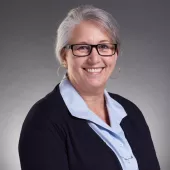
YES (Yield Engineering Systems, Inc.), a leading manufacturer of process equipment for semiconductor advanced packaging, life sciences, and “More-than-Moore” applications, today announced that Prabhat Mishra will be the company’s new Vice President of Finance.
“Prabhat joined the company in August of 2019 as our Head of Finance,” said Ramakanth Alapati, CEO of YES. “Over the past two years, his efforts have been instrumental in helping us manage our rapid trajectory from small-scale manufacturer to preferred supplier for the world’s largest technology companies.”
Prior to joining YES, Mr. Mishra was Senior Director of Finance at Macom and Applied Micro, managing the Financial Planning and Analysis function of the company. Before that, he spent 10 years as a finance leader at Intel Corporation, supporting the Mobile Products Group, the Software & Services Group and the Technology & Manufacturing Group. He started his career as an engineer and was an engineering manager at STMicroelectronics, Sun Microsystems and Intel.
Mr. Mishra holds a bachelor’s degree in Electrical Engineering from the Indian Institute of Technology in Delhi, an MBA from Arizona State University, and Certification in Accounting from University of California, Berkeley.
About YES
YES (Yield Engineering Systems, Inc.) is a preferred provider of high-tech, cost-effective equipment for transforming surfaces, materials and interfaces. The company’s product lines include vacuum cure systems, chemical vapor deposition (CVD) systems, and plasma etching tools used for precise surface modification and thin-film coating of semiconductor wafers, semiconductor and MEMS devices, biosensors and medical substrates. With YES, customers ranging from startups to Fortune 100 companies can create and volume-produce products in a wide range of markets, including Advanced Packaging, MEMS, Augmented Reality/Virtual Reality and Life Sciences. YES is headquartered in Fremont, California, with a growing presence globally. For more information, please visit http://www.yieldengineering.com.