downloadGroupGroupnoun_press release_995423_000000 copyGroupnoun_Feed_96767_000000Group 19noun_pictures_1817522_000000Member company iconResource item iconStore item iconGroup 19Group 19noun_Photo_2085192_000000 Copynoun_presentation_2096081_000000Group 19Group Copy 7noun_webinar_692730_000000Path
Skip to main content
Default Banner Image

SEMI Press Release

ID
semi-press-release

SHANGHAI, China ─ May 18, 2022 ─ SEMI today announced that SEMICON China 2022, originally scheduled for June 15-17 at the National Exhibition and Convention Center (NECC) in Shanghai, has been cancelled due to the ongoing COVID-19 pandemic and related government control measures. As an alternative to the event, the largest and most influential gathering of the semiconductor supply chain in China, SEMI has organized a special edition of SEMICON China, concurrent with FPD China, at the Shanghai New International Expo Center with the following schedule:SEMICON China logo

  • Exhibition: October 5-7, 2022
  • Forums: October 4-7, 2022

With the health and safety of event exhibitors and visitors as top priority, SEMI will continue to follow China government guidelines for pandemic prevention and control. SEMI is in contact with SEMICON China and FPD China exhibitors and sponsors with details about participating in the October events.

About SEMI

SEMI® connects more than 2,500 member companies and 1.3 million professionals worldwide to advance the technology and business of electronics design and manufacturing. SEMI members are responsible for the innovations in materials, design, equipment, software, devices, and services that enable smarter, faster, more powerful, and more affordable electronic products. Electronic System Design Alliance (ESD Alliance), FlexTech, the Fab Owners Alliance (FOA), the MEMS & Sensors Industry Group (MSIG) and SOI Consortium are SEMI Strategic Technology Communities. Visit www.semi.org to learn more, contact one of our worldwide offices, and connect with SEMI on LinkedIn and Twitter.

Association Contact

Cherry Sun
SEMI China
Email: [email protected] 
Phone: +86.21.6027.8548

MILPITAS, Calif. — May 17, 2022 — SEMI, the global industry association that unites the entire electronics manufacturing and design supply chain, and the UCLA Center for Heterogeneous Integration and Performance Scaling (UCLA CHIPS) today announced that they have won a $300,000 grant from the U.S. Department of Commerce’s National Institute of Standards and Technology (NIST) to produce a roadmap for advancing heterogeneous integration and advanced packaging technologies in the United States.

SEMI logoThe roadmap will build upon the International Technology Roadmap for Semiconductors (ITRS) and Heterogeneous Integration Roadmap (HIR) by translating the HIR into a blueprint that defines requirements for rolling out the roadmap in U.S. semiconductor factories. The grant, one of the first awarded by NIST's Advanced Manufacturing Technology Roadmap Program (MfgTech), will fund the project for 18 months.

Supported by microelectronics leaders, SEMI and UCLA CHIPS will create a technology-neutral communications platform for peers across the supply chain, academics and industry experts. SEMI will also define a process for prioritizing and guiding critical areas of the HIR to standardization, while UCLA will organize academically themed workshops and panels to ensure the roadmaps are scalable and extendible as new applications evolve and new processes are developed.

“While the Heterogeneous Integration Roadmap is application-focused, our work will translate this roadmap into a manufacturing infrastructure blueprint that starts at the basic materials used in advanced packaging and breaks down integrated processes into individual unit processes,” said Dr. Subramanian Iyer, distinguished professor of electrical and computer engineering and director of UCLA CHIPS, which is housed at the UCLA Samueli School of Engineering. “Some of them will diverge from traditional silicon processes and include custom manufacturing tools and processes that address dies, wafers and panels. Our roadmap will also be customizable to work with many application-dependent variables."

“SEMI and UCLA CHIPS look forward to leveraging our expertise in semiconductor and packaging roadmaps – from upstream innovations to downstream manufacturing infrastructure – to develop the HIR and take the next step toward factory implementation,” said Dr. Melissa Grupen-Shemansky, SEMI CTO and Vice President of SEMI Technology Communities. “SEMI will also turn to its workforce development strategies to offer heterogeneous integration technology training at all levels of education to meet the growing need for advanced packaging talent in the U.S.” 


About UCLA
As the No. 1 public research university, our mission is the creation, dissemination, preservation and application of knowledge for the betterment of our global society. Located by the Pacific Coast in Los Angeles, we have over 40,000 students enrolled in degree and graduate studies. The university prides itself on a vibrant student body and alumni network that is active in communities around the world.

About SEMI

SEMI® connects more than 2,500 member companies and 1.3 million professionals worldwide to advance the technology and business of electronics design and manufacturing. SEMI members are responsible for the innovations in materials, design, equipment, software, devices, and services that enable smarter, faster, more powerful, and more affordable electronic products. Electronic System Design Alliance (ESD Alliance), FlexTech, the Fab Owners Alliance (FOA), the MEMS & Sensors Industry Group (MSIG) and SOI Consortium are SEMI Strategic Technology Communities. Visit www.semi.org to learn more, contact one of our worldwide offices, and connect with SEMI on LinkedIn and Twitter.

Association Contact   

Michael Hall/SEMI
Phone: 1.408.943.7988
Email: [email protected]

MILPITAS, Calif. — May 4, 2022 — SEMI today announced the promotion of 20-year SEMI veteran Paul Trio to Director of the SEMI International Standards program, effective immediately. Trio will lead the global SEMI Standards staff in managing the industry committees, task force and group meetings, balloting and processes for creating SEMI Standards, with particular emphasis on growing the coverage of the standards. Trio succeeds James Amano, who is transitioning to lead the SEMI Sustainability Initiative.

SEMI logoTrio will report to Dr. Melissa Grupen-Shemansky, SEMI CTO and Vice President of SEMI Technology Communities.

“Paul’s expertise in creating standards to help meet pressing semiconductor industry challenges makes him a strong leader entering the next 50 years of SEMI Standards,” Grupen-Shemansky said. “He has deep working knowledge of the SEMI Standards ratification process, the engineering considerations necessary to prepare standards for adoption, and the importance of involving all key stakeholders. Under Paul’s leadership, we look forward to continuing to advance standards in vital areas across the semiconductor supply chain including traceability, data management, cybersecurity, and emerging technologies such as heterogeneous integration.”

Trio most recently lead several SEMI technology communities including the Collaborative Alliance for Semiconductor Test (CAST) and Semiconductor, Components and Instrumentation and Subsystems (SCIS). He spearheaded the collaboration of these groups, comprised of the leading IC device makers and equipment suppliers, on topics such as traceability and zero defects. 

Trio began his career at SEMI in SEMI Standards, managing committees such as Environmental Health and Safety (EHS), Information & Control (I&C), and Physical Interfaces and Carriers (PIC) before his promotion to lead the North America Standards staff. Trio holds an MBA, Master of Science degree in System Engineering and an undergraduate degree in Electrical Engineering from San Jose State University.

SEMI Standards has published more than 1,000 standards and will celebrate its 50th anniversary since the original M1 Standard was published in 1973. The standard established wafer specifications, enabling the semiconductor industry to innovate the processes needed to create smaller transistors with greater precision. Learn more about SEMI International Standards.  

About SEMI

SEMI® connects more than 2,500 member companies and 1.3 million professionals worldwide to advance the technology and business of electronics design and manufacturing. SEMI members are responsible for the innovations in materials, design, equipment, software, devices, and services that enable smarter, faster, more powerful, and more affordable electronic products. Electronic System Design Alliance (ESD Alliance), FlexTech, the Fab Owners Alliance (FOA), the MEMS & Sensors Industry Group (MSIG) and SOI Consortium are SEMI Strategic Technology Communities. Visit www.semi.org to learn more, contact one of our worldwide offices, and connect with SEMI on LinkedIn and Twitter.

Association Contact

Michael Hall/SEMI
Phone: 1.408.943.7988
Email: [email protected]

MILPITAS, Calif. – April 28, 2022 – Unisem, a global provider of semiconductor assembly and test services, has won the Packaging Process Showdown at MEMS & Sensors Technical Congress (MSTC) for its presentation MEMS Cavity Packages —The Applications, Options and Considerations. Unisem was chosen by more than 100 conference attendees gathered April 26-27 at the David Brower Center in Berkeley, California for insights into the latest MEMS and sensors trends and innovations. SEMI MEMS & Sensors Industry Group (MSIG) stages the event.

MSTC logoAlan Evans, MEMS business development manager at Unisem, detailed the advantages of cavity packages and the wide variety of applications they support. Unisem joined Amkor Technology and Promex Industries at MSTC 2022 in showcasing unique designs and effective packaging techniques to meet the needs of a wide range of MEMS and sensors customers.

Roger Flynn, manager of MEMS and Sensor Products at Amkor, described the company’s platforms and building blocks that incorporate multiple sensors into a single package, while Richard Otte, president of Promex Industries, detailed his company’s approach and solutions to addressing MEMS assembly issues.

“Congratulations to Unisem, Amkor Technology, and Promex Industries for an enlightening and energetic Showdown,” said Tim Brosnihan, executive director of SEMI MSIG. “While winning is noteworthy, competing was really the accomplishment. MSTC attendees enjoyed lending their voices to an unscientific vote on the MEMS packaging process ideas that appeals most to their sense of what the market needs. The Showdown exemplifies how SEMI MSIG meets the needs of our members with timely technical and market insights.”

MSTC is an annual technical event that gathers technical experts in the field. Its sister events, MEMS & Imaging Sensors Summit (September 6-8, 2022 in Grenoble, France) and the MEMS & Sensors Executive Congress (October 11-13, 2022 in San Diego, California), also highlight MEMS and sensors business trends and market opportunities.                       

About SEMI

SEMI® connects more than 2,500 member companies and 1.3 million professionals worldwide to advance the technology and business of electronics design and manufacturing. SEMI members are responsible for the innovations in materials, design, equipment, software, devices, and services that enable smarter, faster, more powerful, and more affordable electronic products. Electronic System Design Alliance (ESD Alliance), FlexTech, the Fab Owners Alliance (FOA), the MEMS & Sensors Industry Group (MSIG) and SOI Consortium are SEMI Strategic Technology Communities. Visit www.semi.org to learn more, contact one of our worldwide offices, and connect with SEMI on LinkedIn and Twitter.

Association Contact   

Michael Hall/SEMI
Phone: 1.408.943.7988
Email: [email protected]

MILPITAS, Calif. — May 2, 2022 — More than 65 industry experts will deliver technical presentations on the latest manufacturing strategies and methodologies as SEMI Advanced Semiconductor Manufacturing Conference (ASMC 2022) opens today in Saratoga Springs, New York. Topics ranging from yield management and metrology to new developments in improving post-pandemic manufacturing agility will take center stage at the May 2-5 event.

ASMCDrawing hundreds of attendees from across the industry, the 33rd annual ASMC features discussions on topics including the global COVID-19 pandemic’s impact on manufacturing leadership, semiconductor market trends, heterogenous integration and quantum computing. ASMC is the premier event for industry professionals to network and share insights into best practices for semiconductor manufacturing.

ASMC 2022 Keynotes and Invited Presentations

Bu

Dr. Huiming Bu, Vice President, Hybrid Cloud Technology Research & Albany Operation, IBM Research

The Future of Semiconductors: Chips and Chiplets

IBM
Hanford

Deirdre Hanford, Chief Security Officer, Synopsys 

Product Innovation and the Acceleration of Design: Demand Drivers on a Secure and Resilient Supply Chain

Synopsys
Baire

Robert Maire, President, Semiconductor Advisors

Emerging Trends in the Global Semiconductor Market


Loubet

Dr. Nicolas Loubet, Senior Technical Staff Member, Advanced CMOS Logic, IBM Research

Nanosheet Tutorial

IBM


ASMC 2022 technical sessions will cover topics including:

  • Advanced Process Control
  • Advanced Equipment Processes and Materials
  • Advanced Metrology
  • Advanced Semiconductor Developments
  • Contamination Free Manufacturing
  • Defect Inspection
  • Equipment Optimization
  • Factory Automation/Industrial Engineering/Smart Manufacturing
  • Yield Enhancement/Yield Management

ASMC will also feature the panel discussion Big Data and Artificial Intelligence for Operations Management in Advanced Semiconductor Manufacturing Industry.

The Women in Semiconductors (WiS 2022) program, to be held today in conjunction with ASMC 2022, will address mentorship, sponsorship and creating a culture of support for women in management and leadership. Complimentary WiS 2022 registration is available for ASMC 2022 attendees. 

ASMC 2022 is co-chaired by Dr. Jean Wynne of IBM and Dr. Shubhodeep Goswami of GE Research.  

For more conference details, contact Paul Cohen at [email protected].                              

About SEMI

SEMI® connects more than 2,500 member companies and 1.3 million professionals worldwide to advance the technology and business of electronics design and manufacturing. SEMI members are responsible for the innovations in materials, design, equipment, software, devices, and services that enable smarter, faster, more powerful, and more affordable electronic products. Electronic System Design Alliance (ESD Alliance), FlexTech, the Fab Owners Alliance (FOA), the MEMS & Sensors Industry Group (MSIG) and SOI Consortium are SEMI Strategic Technology Communities. Visit www.semi.org to learn more, contact one of our worldwide offices, and connect with SEMI on LinkedIn and Twitter.

Association Contact

Michael Hall/SEMI
Phone: 1.408.943.7988
Email: [email protected]

MILPITAS, Calif. — May 2, 2022 — Worldwide silicon wafer area shipments in the first quarter of 2022 surpassed the previous record high set in the third quarter of 2021, rising 1% quarter-over-quarter to 3,679 million square inches, according to the SEMI Silicon Manufacturers Group (SMG) in its quarterly analysis of the silicon wafer industry. First-quarter 2022 silicon wafer shipments saw 10% growth from the 3,337 million square inches reported during the same quarter last year.

SEMI logo“This new silicon shipping milestone points to continued growth in all areas of the semiconductor market,” said Anna-Riikka Vuorikari-Antikainen, Chairman of SEMI SMG and Chief Commercial Officer at Okmetic. “Silicon wafer supply remains tight and may stay constrained with many new announced semiconductor fab investments.”


Silicon Area Shipment Trends – Semiconductor Applications Only


Millions of Square Inches


4Q 2020

1Q 2021

2Q 2021

3Q 2021

4Q 2021

1Q 2022

Total

3,200

3,337

3,534

3,649

3,645

3,679

Source: SEMI (www.semi.org), May 2022


Data cited in this release include polished silicon wafers such as virgin test and epitaxial silicon wafers, as well as non-polished silicon wafers shipped to end users.

Silicon wafers are the fundamental building material for the majority of semiconductors, which are vital components of all electronics including computers, telecommunications products, and consumer devices. The highly engineered thin disks are produced in diameters of up to 12 inches and serve as the substrate material on which most semiconductor devices, or chips, are fabricated.

The SMG is a sub-committee of the SEMI Electronic Materials Group (EMG) and is open to SEMI members involved in manufacturing polycrystalline silicon, monocrystalline silicon or silicon wafers (e.g., as cut, polished, epi). The SMG facilitates collective efforts on issues related to the silicon industry including the development of market information and statistics about the silicon industry and the semiconductor market.

For more information, please visit SEMI Worldwide Silicon Wafer Shipment Statistics.

About SEMI

SEMI® connects more than 2,500 member companies and 1.3 million professionals worldwide to advance the technology and business of electronics design and manufacturing. SEMI members are responsible for the innovations in materials, design, equipment, software, devices, and services that enable smarter, faster, more powerful, and more affordable electronic products. Electronic System Design Alliance (ESD Alliance), FlexTech, the Fab Owners Alliance (FOA), the MEMS & Sensors Industry Group (MSIG) and SOI Consortium are SEMI Strategic Technology Communities. Visit www.semi.org to learn more, contact one of our worldwide offices, and connect with SEMI on LinkedIn and Twitter.

Association Contact

Michael Hall/SEMI
Phone: 1.408.943.7988
Email: [email protected]

MILPITAS, Calif. — April 26, 2022 — FLEX Conference will gather industry experts July 11-14, 2022, at the Moscone Center in San Francisco for keynotes, panel discussions, technical sessions and product-based demonstrations highlighting the latest innovations in flexible and printed electronics. The event will co-locate with SEMICON West Hybrid, North America’s premier microelectronics exhibition and conference that unites players across the entire electronics manufacturing and design supply chain. Registration for both events is open.  

logoThemed Electronics in Motion, FLEX Conference 2022 will focus on equipment, processes, materials and applications driving the latest flexible hybrid electronics (FHE) technology breakthroughs. The event will also showcase innovations emerging from public-private partnerships formed by SEMI Technology Communities SEMI-FlexTech, SEMI-NBMC (Nano-Bio Materials Consortium) and SEMI-NextFlex.

“FLEX Conference has consistently helped turn great ideas into game-changing applications for smart transportation, buildings and infrastructure; equipment sensorization; wearable and conformable medical devices; and more,” said Dr. Melissa Grupen-Shemansky, SEMI CTO and vice president of SEMI Technology Communities. “We are excited to co-locate FLEX with SEMICON West Hybrid to advance the integration of traditional rigid electronics with flexible electronics to improve the way the world works and lives.”

Advances in sustainability across both industries will come into focus at the Global Sustainability Summit at SEMICON West Hybrid and FLEX as flexible electronics combine new levels of processing and sensing capability with improved power usage to make the devices more eco-friendly.

FLEX Conference 2022 Keynote (More keynotes to be announced.)

Headshot

Dr. Michael D. McCreary, Chief Innovation Officer, Senior VP, E Ink Corporation

Electrophoretic Display Technology Will Change the Look of Automobiles, Transportation and Beyond

Eink logo


FLEX Conference 2022 Breakout Sessions

  • FHE Applications
  • Flexible MedTech and Wearables
  • Printing and Processing
  • Reliability and Inspection
  • Strategies and Sustainability
  • Flexible Conductive Materials and Inks
  • Flexible Power
  • FHE Processing and Integration

The Design Automation Conference (DAC), the largest meeting in the electronic design automation (EDA) industry, will also co-locate with SEMICON West Hybrid 2022. Registration for the event is open.

About SEMI

SEMI® connects more than 2,500 member companies and 1.3 million professionals worldwide to advance the technology and business of electronics design and manufacturing. SEMI members are responsible for the innovations in materials, design, equipment, software, devices, and services that enable smarter, faster, more powerful, and more affordable electronic products. Electronic System Design Alliance (ESD Alliance), FlexTech, the Fab Owners Alliance (FOA), the MEMS & Sensors Industry Group (MSIG) and SOI Consortium are SEMI Strategic Technology Communities. Visit www.semi.org to learn more, contact one of our worldwide offices, and connect with SEMI on LinkedIn and Twitter.

Association Contact   

Michael Hall/SEMI
Phone: 1.408.943.7988
Email: [email protected]

Posthumous Recognition for Individuals who made Significant Contributions to Industry

MILPITAS, Calif. –– April 25, 2022 –– The nomination deadline for the Phil Kaufman Hall of Fame for Distinguished Contributions to Electronic System Design has been extended to Friday, May 27, the Electronic System Design Alliance (ESD Alliance) and the IEEE Council on Electronic Design Automation (CEDA), sponsors of the honor, announced today.

The honor posthumously recognizes individuals who made significant contributions to the industry and were not recipients of the Phil Kaufman Award. Deceased members of the community are not eligible to receive the Phil Kaufman Award, a policy set by the IEEE.

SEMI ESDA CEDA logo


Inaugural honorees awarded in 2021 were Jim Hogan, executive, angel investor and board member, and Stanford University Professor Edward J. McCluskey, acknowledged for their significant and noteworthy contributions.

Selections for entry are determined through a nomination process and reviewed by the ESD Alliance and IEEE CEDA Kaufman Award selection committees. A special Phil Kaufman Hall of Fame page on the ESD Alliance and IEEE CEDA websites will host photos, citations and tributes to the selected inductees.

Inductees will be announced in June. The link to the nomination form can be found here. Nominations submitted in 2021 will be valid through 2023.

About the Electronic System Design Alliance

The Electronic System Design (ESD) Alliance, a SEMI Technology Community representing members in the electronic system and semiconductor design ecosystem, is a community that addresses technical, marketing, economic and legislative issues affecting the entire industry. It acts as the central voice to communicate and promote the value of the semiconductor design ecosystem as a vital component of the global electronics industry. Visit www.semi.org/en/communities/esda to learn more.

Follow the ESD Alliance

ESD Alliance Bridging the Frontier blog
Twitter: @ESDAlliance
LinkedIn
Facebook

About SEMI

SEMI® connects more than 2,500 member companies and 1.3 million professionals worldwide to advance the technology and business of electronics design and manufacturing. SEMI members are responsible for the innovations in materials, design, equipment, software, devices, and services that enable smarter, faster, more powerful, and more affordable electronic products. Electronic System Design Alliance (ESD Alliance), FlexTech, the Fab Owners Alliance (FOA), the MEMS & Sensors Industry Group (MSIG) and SOI Consortium are SEMI Strategic Technology Communities. Visit www.semi.org to learn more, contact one of our worldwide offices, and connect with SEMI on LinkedIn and Twitter.

About the IEEE Council on Electronic Design Automation (CEDA)

The IEEE Council on Electronic Design Automation (CEDA) provides a focal point for EDA activities spread across seven IEEE societies (Antennas and Propagation, Circuits and Systems, Computer, Electron Devices, Electronics Packaging, Microwave Theory and Techniques, and Solid-State Circuits). The Council sponsors or co-sponsors over a dozen key EDA conferences including: the Design Automation Conference (DAC), Asia and South Pacific Design Automation Conference (ASP-DAC), International Conference on Computer-Aided Design (ICCAD), Design Automation and Test in Europe (DATE), and events at Embedded Systems Week (ESWEEK). The Council also publishes IEEE Transactions on Computer-Aided Design of Integrated Circuits & Systems (TCAD), IEEE Design & Test (D&T), and IEEE Embedded Systems Letters (ESL). The Council boasts a prestigious awards program in order to promote the recognition of leading EDA professionals, which includes the A. Richard Newton, Phil Kaufman, and Ernest S. Kuh Early Career Awards. The Council welcomes new volunteers and local chapters.

Stay in touch with IEEE CEDA

Website: www.ieee-ceda.org
LinkedIn: https://www.linkedin.com/groups/8343531Facebook: https://www.facebook.com/ieeeceda/Twitter: https://twitter.com/IEEECEDA
 

All trademarks and registered trademarks are the property of their respective owners.


Association Contacts

Nanette Collins                                                                                                          
Public Relations for the ESD Alliance                                   
Email: [email protected]       

Michael Hall/SEMI
Email: [email protected]

Amanda Osborn
IEEE Council on EDA
[email protected]

MILPITAS, Calif. – April 12, 2022 – Worldwide sales of semiconductor manufacturing equipment in 2021 surged 44% to an all-time record of $102.6 billion from $71.2 billion in 2020, SEMI, the industry association representing the global electronics product design and manufacturing supply chain, reported today. The data is now available in the Worldwide Semiconductor Equipment Market Statistics (WWSEMS) Report.

SEMI logoChina claimed the largest market for semiconductor equipment for the second time with sales expanding 58% to $29.6 billion to mark the fourth consecutive year of growth. Korea, the second-largest equipment market, registered a sales increase of 55% to $25.0 billion, after showing strong growth in 2020. Taiwan logged 45% growth to $24.9 billion to claim the third position. Annual semiconductor equipment spending increased 23% in Europe and 17% in North America, which continues to recover from a contraction in 2020. Sales in Rest of the World jumped 79% in 2021.

“The 44% increase in manufacturing equipment spending in 2021 highlights the global semiconductor industry’s aggressive push to add capacity,” said Ajit Manocha, SEMI president and CEO. “This drive to expand production capabilities extends beyond the current supply imbalance, as the industry continues to ramp up to address a wide range of emerging high-tech applications that will enable a smarter digital world with countless social benefits.”

Global sales of wafer processing equipment rose 44% in 2021, while other front-end segment sales grew 22%. Assembly and packaging showed exceptional growth across all regions, resulting in an 87% market increase in 2021, while total test equipment sales rose 30%.

Compiled from data submitted by members of SEMI and the Semiconductor Equipment Association of Japan (SEAJ), the Worldwide SEMS Report is a summary of the monthly billings figures for the global semiconductor equipment industry. Equipment categories cover wafer processing, assembly and packaging, test, and other front-end equipment including mask/reticle manufacturing, wafer manufacturing, and fab facilities.

Annual Billings by Region in Billions of U.S. Dollars with Year-Over-Year Change Rates

Region

2021

2020

% Change

China

29.62

18.72

58%

Korea

24.98

16.08

55%

Taiwan

24.94

17.15

45%

Japan

7.80

7.58

3%

North America

7.61

6.53

17%

Rest of the World

4.44

2.48

79%

Europe

3.25

2.64

23%

Total

102.64

71.19

44%

Source: SEMI (www.semi.org) and SEAJ (www.seaj.or.jp), April 2022


The SEMI Equipment Market Data Subscription (EMDS) provides comprehensive market data for the global semiconductor equipment market. The subscription includes three reports:

  • Monthly SEMI Billings Report, a perspective on equipment market trends
  • Monthly Worldwide Semiconductor Equipment Market Statistics (WWSEMS), a detailed report of semiconductor equipment billings for seven regions and 24 market segments
  • SEMI Semiconductor Equipment Forecast, an outlook for the semiconductor equipment market

For more information or to subscribe, please contact the SEMI Industry Research and Statistics Group at [email protected]. More information is also available online.


About SEMI
SEMI® connects more than 2,500 member companies and 1.3 million professionals worldwide to advance the technology and business of electronics design and manufacturing. SEMI members are responsible for the innovations in materials, design, equipment, software, devices, and services that enable smarter, faster, more powerful, and more affordable electronic products. Electronic System Design Alliance (ESD Alliance), FlexTech, the Fab Owners Alliance (FOA), the MEMS & Sensors Industry Group (MSIG) and SOI Consortium are SEMI Strategic Technology Communities. Visit www.semi.org to learn more, contact one of our worldwide offices, and connect with SEMI on LinkedIn and Twitter.

Association Contact
Michael Hall/SEMI
Phone: 1.408.943.7988
Email: [email protected]

MILPITAS, Calif. — April 11, 2022 — Semiconductor manufacturers worldwide are on track to boost 200mm fab capacity by 1.2 million wafers, or 21%, from the start of 2020 to the end of 2024 to hit a record high of 6.9 million wafers per month, SEMI announced today in its 200mm Fab Outlook Report. After climbing to $5.3 billion last year, 200mm fab equipment spending is expected to be $4.9 billion in 2022 as 200mm fab utilization remains at high levels and the global semiconductor industry works to overcome the chip shortage.

SEMI logo“Wafer manufacturers will add 25 new 200mm lines over the five-year period to help meet growing demand for applications such as 5G, automotive and Internet of Things (IoT) devices that rely on devices like analog, power management and display driver integrated circuits (ICs), MOSFETs, microcontroller units (MCUs) and sensors,” said Ajit Manocha, SEMI president and CEO.
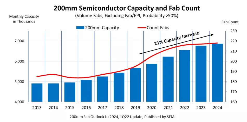
The SEMI 200mm Fab Outlook Report, covering the 12 years from 2013 to 2024, also reveals that foundries will account for more than 50% of fab capacity worldwide this year, followed by analog at 19% and discrete/power at 12%. Regionally, China will lead the world in 200mm capacity with 21% share in 2022, followed by Japan with 16% and Taiwan and Europe/Mideast at 15% each.
 

200mm Fab Report chart

200mm installed semiconductor capacity and fab count, 2013 to 2024*


* Fab count is net of wafer-size conversions.


Equipment investments are projected to remain above $3 billion in 2023, with the foundry sector accounting for 54%, followed by discrete/power at 20% and analog at 19%.

The SEMI 200mm Fab Outlook Report lists more than 330 fabs and lines and includes 64 changes across 47 fabs since its most recent update in September 2021.

About SEMI

SEMI® connects more than 2,500 member companies and 1.3 million professionals worldwide to advance the technology and business of electronics design and manufacturing. SEMI members are responsible for the innovations in materials, design, equipment, software, devices, and services that enable smarter, faster, more powerful, and more affordable electronic products. Electronic System Design Alliance (ESD Alliance), FlexTech, the Fab Owners Alliance (FOA), the MEMS & Sensors Industry Group (MSIG) and SOI Consortium are SEMI Strategic Technology Communities. Visit www.semi.org to learn more, contact one of our worldwide offices, and connect with SEMI on LinkedIn and Twitter.

Association Contacts

Michael Hall/SEMI
Phone: 1.408.943.7988
Email: [email protected]

Christian G. Dieseldorff/SEMI
Phone: 1.408.943.7940
Email: [email protected]