downloadGroupGroupnoun_press release_995423_000000 copyGroupnoun_Feed_96767_000000Group 19noun_pictures_1817522_000000Member company iconResource item iconStore item iconGroup 19Group 19noun_Photo_2085192_000000 Copynoun_presentation_2096081_000000Group 19Group Copy 7noun_webinar_692730_000000Path
Skip to main content
Default Banner Image

SEMI Press Release

ID
semi-press-release

HSINCHU, Taiwan – December 27, 2021 – The latest advances in compound semiconductors, heterogeneous integration, smart manufacturing and green manufacturing will take center stage December 28-30 at SEMICON Taiwan 2021 as industry leaders and visionaries gather at the Nangang Exhibition Center, Hall I (TaiNEX 1) for the latest innovations and trends driving microelectronics industry growth. Registration is open for the region’s premier event for the electronics manufacturing supply chain in Taiwan.

SEMICON Taiwan logoSEMICON Taiwan 2021 will feature more than 650 exhibitors at nearly 2,150 booths. Semiconductor industry giants including TSMC, Etron Technology, ASE, SPIL, WIN Semiconductors, Nanya Technology, PSMC , Unimicron, TEL, Applied Materials, ASM, Lintec, Hermes Epitek and DuPont and other leaders across the semiconductor supply chain will demonstrate innovations powered by cutting-edge technologies including artificial intelligence (AI), Internet of Things (IoT) and 5G.

“The global semiconductor market is projected to grow more than 20% with Taiwan's integrated circuit (IC) production expected to top NT$4 trillion in 2021,” said Terry Tsao, Global Chief Marketing Officer at SEMI and president of SEMI Taiwan. “To help fuel that growth, SEMICON Taiwan 2021 will feature business matching and other opportunities for the industry to drive innovations across advanced semiconductor manufacturing, advanced testing and strategic materials, and enhance its sustainability and environmental, social and governance (ESG) efforts while addressing other areas key to the ongoing industry expansion.”

Themed Exhibitions at SEMICON Taiwan 2021

Themed Forward as One, SEMICON Taiwan 2021 will feature the following four themed exhibitions while promoting Taiwan’s semiconductor industry development policies. New pavilions focusing on investment in Central Taiwan Science Park (Taichung) and Southern Taiwan Science Park (Tainan and Kaohsiung) will also highlight the event. 

  • Compound Semiconductor Innovation Zone – Leading companies such as WIN Semiconductors, IQE, Applied Materials and Hermes Epitek will highlight end-user applications of 5G, 3D sensing, lidar and radar, and powertrain. At SEMI Talks, experts from GaN Systems, UMC, Episil and National Taiwan University will explore Taiwan's competitive advantages in wide-bandgap (WBG) semiconductors. More than 10 leading companies will offer a deep dive into trends and breakthroughs enabled by compound semiconductor materials such as gallium arsenide (GaAs), gallium nitride (GaN), and silicon carbide (SiC).
  • Heterogeneous Integration Innovation Zone – With the rise of 5G, AI and other leading-edge technologies increasing requirements for packaging and transistors extending beyond size limits, game-changing heterogeneous packaging technologies have emerged to fuel semiconductor advances to extend Moore’s law. ASE, SPIL and other leading players will showcase high-performance computing (HPC) technology, along with IC design, manufacturing, packaging and terminal system applications. Chiplets, 3D stacking, and substrate design will come into sharp focus.
  • Smart Manufacturing Journey – Staged by ADLINK, AWS Taiwan, Beckhoff, FET, Siemens, and TM Robot, this hands-on interactive experience of the latest smart manufacturing solutions through virtual reality (VR) will showcase drone, AR smart glasses, and IoT applications. The exhibition will also promote the adoption of HPC in semiconductor manufacturing sites to improve yield and production capacity and facilitate digital transformation. In addition, its Cybersecurity Pavilion will address critical topics including hacker attacks; viruses; and cybersecurity drills, maturity evaluation and industry standards with the aim to enhance cybersecurity across the supply chain.
  • Green Manufacturing Innovation Zone (New) – Demonstrating Taiwan’s commitment to sustainable development, this zone will gather technology giants such as TSMC, ASE, Nanya Technology, and PSMC to highlight innovative green manufacturing technologies and front-end applications. Success stories on green design, energy management, resource regeneration, and supply chain resilience will also be featured. In collaboration with the Taiwan semiconductor community, SEMI will launch its Semiconductor Industry ESG Sustainability Initiative, aimed at strengthening the industry’s sustainability strategies and demonstrating Taiwan’s commitment to sustainable manufacturing.

Workforce Development Pavilion

SEMICON Taiwan 2021 will connect young talent with career opportunities as industry leaders including TSMC, Applied Materials, ASE, ASML, DuPont, Entegris, Lam Research, Merck KGaA, Darmstadt, Germany, Micron and TEL discuss talent development trends and career planning insights. The Workforce Development Pavilion will feature one-on-one talent matching and discussions on key topics including diversity and inclusion, women in technology and creating winning talent strategies.


About SEMI

SEMI® connects more than 2,400 member companies and 1.3 million professionals worldwide to advance the technology and business of electronics design and manufacturing. SEMI members are responsible for the innovations in materials, design, equipment, software, devices, and services that enable smarter, faster, more powerful, and more affordable electronic products. Electronic System Design Alliance (ESD Alliance), FlexTech, the Fab Owners Alliance (FOA) and the MEMS & Sensors Industry Group (MSIG) are SEMI Strategic Technology Communities, defined communities within SEMI focused on specific technologies. Visit www.semi.org to learn more, contact one of our worldwide offices, and connect with SEMI on LinkedIn and Twitter.


Media Contacts

SEMI Taiwan

Ashley Huang

(03)560-1777 Ext.206

[email protected]


SEMI Taiwan

Connie Lin

(03)560-1777 Ext.211

[email protected]


Ogilvy PR

Ashley Lu

(02)7745-1557

[email protected]

MILPITAS, Calif. — December 20, 2021 — North America-based semiconductor equipment manufacturers posted $3.93 billion in billings worldwide in November 2021 (three-month moving average basis), according to the November Equipment Market Data Subscription (EMDS) Billings Report published today by SEMI. The billings figure is 5.0% higher than final October 2021 billings of $3.74 billion and 50.6% higher than November 2020 billings of $2.61 billion.

SEMI logo“Billings of North America-based semiconductor equipment manufacturers extended a robust uptrend to reach another new record in November,” said Ajit Manocha, president and CEO of SEMI.  “Industry performance remains unprecedented despite persistent supply chain challenges.”


The SEMI Billings report uses three-month moving averages of worldwide billings for North American-based semiconductor equipment manufacturers. Billings figures are in millions of U.S. dollars.


Billings
(3-mo. Avg.)

Year-Over-Year

June 2021

$3,690.2

59.2%

July 2021

$3,857.4

49.8%

August 2021

$3,656.3

37.8%

September 2021

$3,718.2

35.5%

October 2021 (final)

$3,745.4

41.4%

November 2021 (prelim)

$3,913.9

50.6%

Source: SEMI (www.semi.org), December 2021


SEMI publishes a monthly North American Billings report and issues the Worldwide Semiconductor Equipment Market Statistics (WWSEMS) report in collaboration with the Semiconductor Equipment Association of Japan (SEAJ). The WWSEMS report currently reports billings by 24 equipment segments and by seven end market regions. SEMI also has a long history of tracking semiconductor industry fab investments in detail on a company-by-company and fab-by-fab basis in its World Fab Forecast and SEMI FabView databases. These powerful tools provide access to spending forecasts, capacity ramp, technology transitions, and other information for over 1,000 fabs worldwide. For an overview of available SEMI market data, please visit www.semi.org/en/MarketInfo.

The data contained in this release were compiled by David Powell, Inc., an independent financial services firm, without audit, from data submitted directly by the participants. SEMI and David Powell, Inc. assume no responsibility for the accuracy of the underlying data.


About SEMI

SEMI® connects more than 2,400 member companies and 1.3 million professionals worldwide to advance the technology and business of electronics design and manufacturing. SEMI members are responsible for the innovations in materials, design, equipment, software, devices, and services that enable smarter, faster, more powerful, and more affordable electronic products. Electronic System Design Alliance (ESD Alliance), FlexTech, the Fab Owners Alliance (FOA) and the MEMS & Sensors Industry Group (MSIG) are SEMI Strategic Technology Communities, defined communities within SEMI focused on specific technologies. Visit www.semi.org to learn more, contact one of our worldwide offices, and connect with SEMI on LinkedIn and Twitter.


Association Contact

Michael Hall/SEMI
Phone: 1.408.943.7988
Email: [email protected]
 

Notes

Next SEMI Billings report is January 25, 2022 at 3:00pm Pacific.

For information on SEAJ Billings Express Report, visit www.seaj.or.jp. 

MILPITAS, Calif. – December 16, 2021 – Dr. Anirudh Devgan, President and CEO of Cadence Design Systems, Inc. has been selected to receive the 2021 Phil Kaufman Award for Distinguished Contributions to Electronic System Design.

The Phil Kaufman Award is presented annually by the Electronic System Design Alliance (ESD Alliance), a SEMI Technology Community, and the IEEE Council on Electronic Design Automation (CEDA). The award ceremony and dinner will be held Thursday, March 10, from 6:30pm to 9:30pm at The GlassHouse in San Jose, California. Registration details will be available soon.
 

SEMI ESDA CEDA logos


Dr. Devgan is being honored for his extensive contributions to electronic design automation (EDA). He is widely recognized as a leading authority in parallel and distributed computing and has made a broad impact in fields ranging from circuit simulation to statistical design and optimization, physical design and signoff, verification and hardware platforms, and system design and analysis. Dr. Devgan’s groundbreaking contributions include not just the development of algorithms, but also successfully bringing to market commercial solutions that have gained widespread customer adoption throughout the industry.

“Anirudh has a truly rare combination of widely recognized research excellence, exceptional business impact and results, and outstanding leadership in the EDA industry,” said Lip-Bu Tan, former CEO and now Executive Chairman of Cadence, who nominated Dr. Devgan for this honor. “Anirudh’s overall contributions during his career spanning Carnegie Mellon, IBM, Magma and Cadence have significantly advanced the industry.”

“I have known Anirudh for over 20 years from his early days at IBM and have since closely followed his spectacular career in the industry,” said Alberto Sangiovanni Vincentelli, The Edgar L. and Harold H. Buttner Chair of EECS, University of California, Berkeley, a Cadence founder and a Kaufmann Award winner. “I know of hardly anyone in EDA who has that winning combination of bold vision and deep technical know-how, along with outstanding leadership and organizational skills. Leveraging these unique abilities, Anirudh has been able to constantly innovate in a mature field like EDA and bring to market a sequence of game-changing products that have delivered transformational business results.”

“On behalf of the ESD Alliance, I would like to congratulate Anirudh on receiving the 2021 Phil Kaufman award,” said Simon Segars, ESD Alliance Chairman and CEO of Arm Holdings. “His contributions in technical innovation have been foundational to bringing the EDA industry into the modern parallel and cloud computing era. Anirudh’s impact on the industry is well-recognized and celebrated with this distinguished honor.”

About Dr. Anirudh Devgan, the 2021 Phil Kaufman Award Recipient

Dr. Devgan joined Cadence in 2012, has served as President of Cadence since 2017 and has been a member of the Cadence Board of Directors since August 2021. He assumed the additional role of Cadence CEO on December 15, 2021.

Dr. Devgan began his career at the IBM Research (Thomas J. Watson Research Center) in 1994. His work at IBM on EDA algorithms and design optimization techniques contributed to IBM’s leadership in the 1990s and 2000s in high-performance microprocessor and server designs. He joined Magma Design Automation in 2005 as a key member of its Executive Management Team and General Manager of the Custom Design Business Unit. He initiated and brought to market multiple new products in the areas of circuit simulation, analog mixed-signal design, physical verification, library characterization and 3D extraction among others. The products were successful in both customer adoption and business results.

At Cadence, Dr. Devgan has spearheaded technology excellence and driven the re-architecture and revamping of its product lines, notably the entire suite of digital and signoff tools, as well as its functional and mixed-signal simulation solutions. Dr. Devgan established Cadence’s Intelligent System Design strategy and is driving breakthrough advancements in cloud, artificial intelligence (AI) and machine learning (ML) and system innovation. Dr Devgan’s leadership and contributions have had a transformational impact, with a significant increase in Cadence’s revenue, profitability and market capitalization as well as in the overall customer and market adoption of its solutions.

Dr. Devgan has received best paper awards from both leading conferences in the field –Design Automation Conference (DAC) and International Conference on Computer Aided Design (ICCAD). Dr. Devgan is an IEEE Fellow, holds 27 U.S. patents and has published numerous research papers in leading journals and conferences. Dr. Devgan received a Bachelor of Technology degree in Electrical Engineering from the Indian Institute of Technology, Delhi, and Master of Science and Ph.D. degrees in Electrical and Computer Engineering from Carnegie Mellon University.

About the Phil Kaufman Award

The Phil Kaufman Award honors individuals who have had a demonstrable impact on the field of electronic system design through technology innovations, education/mentoring, or business or industry leadership. The award was established as a tribute to Phil Kaufman, the late industry pioneer who turned innovative technologies into commercial businesses that have benefited electronic designers. The 2019 recipient was Dr. Mary Jane Irwin, Evan Pugh Professor and A. Robert Noll Chair Emeritus in Engineering in the Department of Computer Science and Engineering at Pennsylvania State University. Due to the COVID-19 pandemic, there was no Phil Kaufman Award in 2020.

About the IEEE Council on Electronic Design Automation (CEDA)

The IEEE Council on Electronic Design Automation (CEDA) provides a focal point for EDA activities spread across seven IEEE societies (Antennas and Propagation, Circuits and Systems, Computer, Electron Devices, Electronics Packaging, Microwave Theory and Techniques, and Solid-State Circuits). The Council sponsors or co-sponsors over a dozen key EDA conferences including: the Design Automation Conference (DAC), Asia and South Pacific Design Automation Conference (ASP-DAC), International Conference on Computer-Aided Design (ICCAD), Design Automation and Test in Europe (DATE), and events at Embedded Systems Week (ESWEEK). The Council also publishes IEEE Transactions on Computer-Aided Design of Integrated Circuits & Systems (TCAD), IEEE Design & Test (D&T), and IEEE Embedded Systems Letters (ESL). The Council boasts a prestigious awards program in order to promote the recognition of leading EDA professionals, which includes the A. Richard Newton, Phil Kaufman, and Ernest S. Kuh Early Career Awards. The Council welcomes new volunteers and local chapters.
 

Stay in touch with IEEE CEDA

Website: www.ieee-ceda.org
LinkedIn: https://www.linkedin.com/groups/8343531
Facebook: https://www.facebook.com/ieeeceda/
Twitter: https://twitter.com/IEEECEDA
 

About the Electronic System Design Alliance

The Electronic System Design (ESD) Alliance, a SEMI Technology Community representing members in the electronic system and semiconductor design ecosystem, addresses technical, marketing, economic and legislative issues affecting the entire industry. It acts as the central voice to communicate and promote the value of the semiconductor design ecosystem as a vital component of the global electronics industry. Visit www.semi.org/en/communities/esda to learn more.
 

Follow the ESD Alliance

ESD Alliance Bridging the Frontier blog
Twitter: @ESDAlliance
LinkedIn
Facebook
 

About SEMI

SEMI® connects more than 2,400 member companies and 1.3 million professionals worldwide to advance the technology and business of electronics design and manufacturing. SEMI members are responsible for the innovations in materials, design, equipment, software, devices, and services that enable smarter, faster, more powerful, and more affordable electronic products. Electronic System Design Alliance (ESD Alliance), FlexTech, the Fab Owners Alliance (FOA) and the MEMS & Sensors Industry Group (MSIG) are SEMI Strategic Technology Communities, defined communities within SEMI focused on specific technologies. Visit www.semi.org to learn more, contact one of our worldwide offices, and connect with SEMI on LinkedIn and Twitter.

All trademarks and registered trademarks are the property of their respective owners.
 

Association Contacts

Nanette Collins
Public Relations for the ESD Alliance                         
Email: [email protected]  
 

Michael Hall/SEMI
Email: [email protected]
 

Amanda Osborn
IEEE Council on EDA
[email protected]

MILPITAS, Calif. — December 14, 2021 — SEMI today announced that Tom Tsuneishi, Chairman of Tokyo Electron, will receive the 2021 SEMI Sales and Marketing Excellence Award, inspired by Bob Graham, for his contributions over his career. The 23rd recipient of the award, Tsuneishi will be honored for his systematic development of market strategies based on an approach that integrated system reliability, market adjacencies, globalization, technology development, and extreme customer support over the last four decades. He will be recognized during ceremonies at SEMICON Japan 2021 Hybrid, December 15-17 at Tokyo Big Sight in Tokyo, and will be presented the award at the Industry Strategy Symposium (ISS) 2022, January 9-12 at Half Moon Bay, California.

SEMI logoAt Tokyo Electron, Tsuneishi drove a mindset transformation of selling beyond Japan-based companies, first developing a strategic vision for investing in global operations in the U.S. and then replicating it in Korea, Taiwan, Europe, Singapore and China. He benefitted customers in these regions by enabling them to deliver better value and cost-of-ownership. By bringing the focus of exceptional Japanese quality to more customers, Tsuneishi helped drive the adoption of these standards worldwide to strengthen and grow the global semiconductor industry. Access to top-notch local technology centers and the delivery of local solutions by service and support organizations underpinned his quality standards.
“SEMI recognizes Tom Tsuneishi for being a true industry statesman who built bridges to connect the global semiconductor industry and raised the bar on delivering quality to customers,” said Ajit Manocha, president and CEO of SEMI. “Tsuneishi-san is a worthy recipient of the SEMI Sales and Marketing Excellence award for his contributions to the industry over his long and illustrious career, and we greatly appreciate that he continues to share his insightful wisdom with the industry as a member of the SEMI International Board of Directors.”

The SEMI Sales and Marketing Excellence Award was inspired by the late Bob Graham, the distinguished semiconductor industry leader, who was a member of the founding team of Intel. Graham also helped industry-leading companies such as Applied Materials and Novellus Systems during their formative years. The award was established to honor individuals for the creation and/or implementation of marketing programs that enhance customer satisfaction and further the growth of the semiconductor equipment and materials industry.

Eligible candidates are nominated by their industry peers and selected after due diligence by the SEMI Sales and Marketing Excellence Award Committee. Previous recipients of this award include: Mitsunobu Koshiba (2019), Luc Van den hove (2018), Toshio Maruyama (2017), Jim Bowen (2016), Terry (Tetsuro) Higashi (2015), Winfried Kaiser (2014), Joung Cho (JC) Kim (2013), G. Dan Hutcheson (2012), Franz Janker (2011), Martin van den Brink (2010), Peter Hanley (2009), Richard Hong (2008), Richard E. Dyck (2007), Aubrey (Bill) C. Tobey (2006), Archie Hwang (2005), Edward Braun (2004), Shigeru (Steve) Nakayama (2003), Jerry Hutcheson and Ed Segal (2002), Jim Healy and Barry Rapozo (2001), and Art Zafiropoulo (2000).


About SEMI

SEMI® connects more than 2,400 member companies and 1.3 million professionals worldwide to advance the technology and business of electronics design and manufacturing. SEMI members are responsible for the innovations in materials, design, equipment, software, devices, and services that enable smarter, faster, more powerful, and more affordable electronic products. Electronic System Design Alliance (ESD Alliance), FlexTech, the Fab Owners Alliance (FOA) and the MEMS & Sensors Industry Group (MSIG) are SEMI Strategic Technology Communities, defined communities within SEMI focused on specific technologies. Visit www.semi.org to learn more, contact one of our worldwide offices, and connect with SEMI on LinkedIn and Twitter.


Association Contact

Michael Hall/SEMI
Phone: 1.408.943.7988
Email: [email protected]

SEOUL, South Korea — December 15, 2021 — With Korea projected to rank among world leaders in semiconductor fab equipment spending next year, the stage is set for SEMICON Korea 2022 Hybrid as more than 450 companies gather February 9-11, 2022 at the COEX in Seoul for insights from visionaries and industry leaders into the latest microelectronics ecosystem developments, innovations and business opportunities. Trends critical to sustaining strong microelectronics industry growth such as smart manufacturing, sensorization, semiconductor design automation, manufacturing sustainability and workforce development will come into sharp focus. Registration for SEMICON Korea, the region’s premier microelectronics event, is open.

SEMICON Korea Hybrid logoFeaturing 2,000 booths, SEMICON Korea 2022 Hybrid will host nearly 120 semiconductor industry experts from around the world at 20 virtual conferences. On-demand conferences will be available until February 25, 2022.

The safety of event exhibitors and attendees remains the top SEMI priority as the world continues work to contain the COVID-19 pandemic. Only exhibitors and attendees who have been vaccinated and submitted a negative PCR test result within 48 hours prior to the event will be admitted to the exhibition hall.

SEMICON Korea 2022 Hybrid Highlights

  • Keynotes – Leaders from Samsung Electronics, ASML, Hyundai Mobis, and IONQ will share insights on major industry issues and cutting-edge semiconductor technology trends, including automotive semiconductors and quantum computing.
  • SEMI Technology Symposium (STS) – Leaders from the semiconductor industry, academia, and research will discuss the latest technologies for key manufacturing segments including Lithography, Materials, Device, Etch, Cleaning & CMP, and Packaging.
  • AI Summit – With artificial intelligence (AI) a key driver of semiconductor industry growth, experts from various fields such as fabless, semiconductor equipment companies, and chipmakers will share AI technology roadmaps and business models.
  • Design Automation Forum – AI and machine learning are emerging as new solutions to complex semiconductor design challenges. Leading electronic design automation (EDA) companies will provide updates on deployments of AI and machine learning in the EDA industry to help optimize chip design quality and productivity.
  • Smart Manufacturing Forum – Smart manufacturing is playing an important role in the semiconductor industry to increase productivity and reduce costs in manufacturing processes. Smart manufacturing leaders will share the current state of smart manufacturing in the semiconductor material field and discuss the latest Industry 4.0 technologies.
  • MEMS & Sensors Summit – Sensorization experts will explore new business and collaboration opportunities as smart cities move closer to reality.
  • Metrology and Inspection (MI) Forum – Technical demands for metrology solutions are increasing as semiconductors become smaller and more advanced. Measurement equipment companies and semiconductor makers will discuss the latest technological trends and challenges in the field of pre- and post-process measurement.
  • Sustainable Manufacturing Forum – Environment, Health, Safety and Sustainability initiatives are rising in importance as the semiconductor industry drives toward a model of more sustainable manufacturing in the face of climate change. Experts will share sustainable manufacturing best practices and achievements across the semiconductor supply chain.
  • Market Trends Forum – Leading IC research firms will provide perspectives and outlooks on U.S.-China geopolitical tensions, reshoring, semiconductor shortages and other key chip industry issues.

Workforce Development

To help build the semiconductor industry talent pipline, chip engineers will offer career development advice to university engineering students in the popular SEMICON Korea Meet the Experts program.

Diversity, Equity and Inclusion

Diversity, Equity and Inclusion are rising in importance as the semiconductor industry continues to grow its workforce. To encourage greater representatation of women, female leaders from high-tech industries will offer perspectives on strengthening diversity during the Women-in-Technology program geared toward women in high technology as well as tech leaders and employees who work with women.

Business Matching

Leading chipmakers including Intel, Kioxia, and Sony will host nearly 30 business meetings with semiconductor equipment, parts and materials companies as part of the Supplier Search Program to provide new business opportunities for the organizations.

Pre-registration for SEMICON Korea 2022 on-site exhibitions and virtual conferences is open until February 4, 2022. By pre-registering, attendees will receive complimentary admission to the exhibition and the early-bird price for an All-in Pass that provides admission to all conferences. With a Keynote Pass, attendees can attend keynotes for free.


About SEMI

SEMI® connects more than 2,400 member companies and 1.3 million professionals worldwide to advance the technology and business of electronics design and manufacturing. SEMI members are responsible for the innovations in materials, design, equipment, software, devices, and services that enable smarter, faster, more powerful, and more affordable electronic products. Electronic System Design Alliance (ESD Alliance), FlexTech, the Fab Owners Alliance (FOA) and the MEMS & Sensors Industry Group (MSIG) are SEMI Strategic Association Partners, defined communities within SEMI focused on specific technologies. Visit www.semi.org to learn more, contact one of our worldwide offices, and connect with SEMI on LinkedIn and Twitter.


Association Contact

Jaegwan Shim/SEMI
Phone: 82.02.531.7804
Email: [email protected]

MILPITAS, Calif. – December 13, 2021 – SEMI announced today the return of the Industry Strategy Symposium (ISS) 2022 to Half Moon Bay, California, January 9-12 for the year’s first executive check-in, offering perspectives from leading analysts, economists, policymakers and technologists on major forces impacting the semiconductor industry. The annual symposium gives business leaders an insightful view to growth trends and industry intelligence, helping ensure that their company business plans and forecasts are based on current market conditions. Registration is now open.

ISS logoThemed Semiconductors Leading a Transforming World, ISS 2022 will build on the return of the global economy to pre-pandemic growth levels in 2021 with expert insights into related trends and industry forecasts. The conference will examine economic, technology, market, business, and geopolitical developments influencing the global electronics manufacturing industry, along with their implications for strategic business decisions.                     

“ISS is the premiere venue for turning insights from visionaries and microelectronics industry leaders on economic, market, geopolitical and technology developments and trends into actionable intelligence,” said David Anderson, president of SEMI Americas and host of ISS. “The event helps equip companies across the semiconductor supply chain with the information they need to fine-tune their operational and sales strategies in order to seize business opportunities in the year ahead.”

ISS 2022 Highlights

Keynote

  • Mark Papermaster, CTO and Executive Vice President, Technology and Engineering, AMD–High Performance and ML: The Engines of Accelerated Solutions

Economic trends and market perspectives affecting the chip industry

  • Carl Riccadonna, Chief Economist, Bloomberg – 2022 Economic Outlook: Has the Tiger Changed Its Stripes?
  • Michael Yang, Senior Director, Semiconductors, Omdia – The Next Cycle of Semiconductors
  • Jan Vardaman, President and Founder, TechSearch International – Advanced Packaging: Key to Next-Generation Silicon’s Economic Success
  • Andrea Lati, Vice President, Market Research, VLSI Research – Semiconductor Manufacturing Trends: Broken Arrow in a Post-global Era with Pandemics
  • Bob Johnson, Vice President, Gartner – Can the Semiconductor Industry Reach $1T Revenue by 2030?
  • Inna Skvortsova, Industry Research & Statistics, SEMI – Semiconductor Materials Market Forecast and Fab Capacity Trends

Discussions on technology, market and application drivers, global perspectives, diversity, and sustainability

  • Featuring top executives from Amazon Web Services, ams OSRAM, ASM International, BCA Research, Boeing, Google, Headgate Partners, IC Knowledge, imec, Intel, JSR Corporation, Lam Research, Micron, National GEM Consortium, NVIDIA, Resilinc, SkyWater Technology, Synopsys and Varian Medical Systems.


About SEMI

SEMI® connects more than 2,400 member companies and 1.3 million professionals worldwide to advance the technology and business of electronics design and manufacturing. SEMI members are responsible for the innovations in materials, design, equipment, software, devices, and services that enable smarter, faster, more powerful, and more affordable electronic products. Electronic System Design Alliance (ESD Alliance), FlexTech, the Fab Owners Alliance (FOA) and the MEMS & Sensors Industry Group (MSIG) are SEMI Strategic Technology Communities, defined communities within SEMI focused on specific technologies. Visit www.semi.org to learn more, contact one of our worldwide offices, and connect with SEMI on LinkedIn and Twitter.

Association Contact

Scott Stevens, for SEMI Americas

Phone: 1.512.288.4050

Email: [email protected]

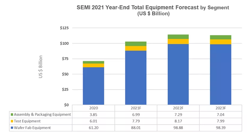
TOKYO — December 14, 2021 — Global sales of total semiconductor manufacturing equipment by original equipment manufacturers are forecast to reach a new high of $103 billion in 2021, surging 44.7% from the previous industry record of $71 billion in 2020, SEMI announced today in releasing its Year-End Total Semiconductor Equipment Forecast – OEM Perspective at SEMICON Japan 2021. The growth is expected to continue with the global total semiconductor manufacturing equipment market expanding to $114 billion by 2022.

“Crossing the $100 billon mark in total semiconductor manufacturing equipment sales reflects the global semiconductor industry’s concerted and exceptional drive to expand capacity to meet strong demand,” said Ajit Manocha, SEMI president and CEO. “We expect continuing investments in the digital infrastructure buildout and secular trends across multiple end markets to fuel healthy growth in 2022.”

SEMI logoBoth the front-end (wafer fab) and back-end (assembly/packaging and test) semiconductor equipment segments are contributing to the global expansion. The wafer fab equipment segment, which includes wafer processing, fab facilities, and mask/reticle equipment, is projected to expand 43.8% to a new industry record of $88 billion in 2021, followed by a 12.4% increase in 2022 to approximately $99 billion. Wafer fab equipment in 2023 is expected to decrease slightly by -0.5% to $98.4 billion.
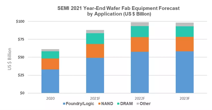

The foundry and logic segments, accounting for more than half of total wafer fab equipment sales, will surge 50% year-over-year to reach $49.3 billion in 2021 driven by demand for both leading-edge and mature nodes. The growth momentum is expected to continue in 2022 with the foundry and logic equipment investments rising 17%.

Strong enterprise and consumer demand for memory and storage is contributing to strength in DRAM and NAND equipment spending. The DRAM equipment segment is leading the expansion in 2021 surging 52% to $15.1 billion and growing 1% in 2022 to $15.3 billion. The NAND equipment market is projected to jump 24% in 2021 to $19.2 billion and 8% in 2022 to $20.6 billion. Expenditures are expected to drop by -2% and -3% in 2023 for DRAM and NAND respectively.

After seeing robust 33.8% growth in 2020, the assembly and packaging equipment segment is expected to surge by 81.7% to $7 billion in 2021, followed by another 4.4% increase in 2022 driven by advanced packaging applications. The semiconductor test equipment market is expected to grow 29.6% in 2021 to $7.8 billion and continue to expand by 4.9% in 2022 on demand for 5G and high-performance computing (HPC) applications.

Regionally, China, Korea, and Taiwan are projected to remain the top three destinations for equipment spending in 2021. China is projected to maintain the top position, which it claimed for the first time in 2020, while Taiwan is expected to regain the top position in the market in 2022 and 2023. Equipment spending for all regions tracked are expected to grow in 2021 and 2022.

The following results reflect market size by segment and application in billions of U.S. dollars:

Year End Chart 1


Year End Chart 2

Source: SEMI December 2021, Equipment Market Data Subscription
 

Total equipment includes new wafer fab, test, and A&P. Total equipment excludes wafer manufacturing equipment. Totals may not add due to rounding.


The current SEMI forecast is based on collective input from top equipment suppliers, the SEMI Worldwide Semiconductor Equipment Market Statistics (WWSEMS) data collection program and the industry-recognized SEMI World Fab Forecast database.

The Equipment Market Data Subscription (EMDS) from SEMI provides comprehensive market data for the global semiconductor equipment market. A subscription includes three reports:

  • Monthly SEMI North American Billings Report, an early perspective of equipment market trends
  • Monthly Worldwide Semiconductor Equipment Market Statistics (WWSEMS), a detailed report of semiconductor equipment billings for seven regions and more than 22 market segments
  • Bi-annual Total Semiconductor Equipment Forecast – OEM Perspective, an outlook for the semiconductor equipment market

For more information online, please visit SEMI Market Data.


About SEMI

SEMI® connects more than 2,400 member companies and 1.3 million professionals worldwide to advance the technology and business of electronics design and manufacturing. SEMI members are responsible for the innovations in materials, design, equipment, software, devices, and services that enable smarter, faster, more powerful, and more affordable electronic products. Electronic System Design Alliance (ESD Alliance), FlexTech, the Fab Owners Alliance (FOA) and the MEMS & Sensors Industry Group (MSIG) are SEMI Strategic Technology Communities, defined communities within SEMI focused on specific technologies. Visit www.semi.org to learn more, contact one of our worldwide offices, and connect with SEMI on LinkedIn and Twitter.

Association Contact

Michael Hall/SEMI
Phone: 1.408.943.7988
Email: [email protected]

TOKYO — December 14, 2021 — SEMICON Japan, the largest and most influential gathering of the electronics manufacturing supply chain in Japan, opens tomorrow at Tokyo Big Sight with a focus on innovation opportunities and business growth potential fueled by leading-edge technologies including 5G, artificial intelligence (AI), deep learning and quantum computing. More than 450 exhibitors will join microelectronics industry leaders and visionaries from across the electronics supply chain at SEMICON Japan 2021 Hybrid, Dec. 15-17, for the latest insights into electronics industry technologies, developments and trends. Registration is open.

SEMICON Japan Hybrid logo“We are excited to be back at Tokyo Big Sight for SEMICON Japan,” said Jim Hamajima, president of SEMI Japan. “For nearly 50 years, SEMICON Japan has gathered companies from across the electronics manufacturing supply chain for the in-person dialog and collaboration critical to innovation and industry growth. I am happy to welcome the industry back to the show floor as we work together to help solve some of the world’s greatest microelectronics challenges and seize tremendous growth opportunities.”

The health and safety of exhibitors and attendees remains a top SEMI priority. SEMI continues to monitor developing national, prefectural and local health and safety recommendations and requirements to implement the most appropriate safety protocols for in-person SEMI events. The COVID-19 infection control guidelines for SEMICON Japan 2021 Hybrid are available on the event website.  

Top executives and technical experts from leading companies and research institutes in Japan and abroad will with share their visions for the industry on the SEMICON Japan 2021 Hybrid online platform. Bilingual service is available for some sessions.  

SEMICON Japan 2021 Hybrid Technology Pavilions

Themed Forward as One, SEMICON Japan 2021 Hybrid features the following pavilions to spotlight leading-edge technologies that are driving semiconductor and electronics demand.  

  • 5G/Post 5G Pavilion with SoftBank
  • COVID-19 Infection Control Pavilion with APPEX, Filtration Group Japan, JFE Techno-Research, NEW COSMOS ELECTRIC, NTK CERATEC, SANEI, Tokyo Dylec, TOKYO KEIKI, Ushio, and Vuzix Corporation
  • FLEX Japan with Elephantech, Innolux Japan, Japan Aviation Electronics Industry, MITSUI CHEMICALS, TOYOBO, Yamagata University YU-FIC, and Zuken
  • Power and Compound Semiconductor Pavilion with Best Compound Semiconductor, EFAB International Technology, FLOSFIA, SiC Alliance, Ion Technology Center, J.A. Woollam Japan, Nippon Precision, and Novel Crystal Technology
  • Quantum Computing Pavilion with blueqat, Hitachi, JSR, and the National Institute of Advanced Industrial Science & Technology
  • Smart Mobility Pavilion with Arm, Floadia, Marvell Semiconductor, Murata Manufacturing, Tokai University, Renesas Electronics, and Zuken

For a detailed schedule, please see the SEMICON Japan Agenda-at-a-Glance.


About SEMI

SEMI® connects more than 2,400 member companies and 1.3 million professionals worldwide to advance the technology and business of electronics design and manufacturing. SEMI members are responsible for the innovations in materials, design, equipment, software, devices, and services that enable smarter, faster, more powerful, and more affordable electronic products. Electronic System Design Alliance (ESD Alliance), FlexTech, the Fab Owners Alliance (FOA) and the MEMS & Sensors Industry Group (MSIG) are SEMI Strategic Association Partners, defined communities within SEMI focused on specific technologies. Visit www.semi.org to learn more, contact one of our worldwide offices, and connect with SEMI on LinkedIn and Twitter.


Association Contact

Hiroki Yomogita

Phone: +81-(0)3-3222-5854

Email: [email protected]

SAN FRANCISCO, Calif. – December 8, 2021​ – Everspin Technologies, a leading worldwide producer of Magnetoresistive random access memory (MRAM) nonvolatile solutions for the world’s mission-critical memory applications, has won the 2021 SEMI Americas Award, SEMI announced today at SEMICON West 2021 Hybrid in San Francisco.

SEMICON West Hybrid logoHeadquarted in Chandler, Arizona, Everspin Technologies was honored for developing the first commercially implemented spin-transfer torque (STT) memory in partnership with GlobalFoundries. The new Everspin 1-gigabayte (GB) STT-MRAM device with a 28nm process is the world’s first in its class. MRAM offers performance characteristics akin to SRAMs, while maintaining its charge and data during system power outages.

Implementation of STT-MRAM memory elements enabled the deployment of a new class of process tools developed by Applied Materials, Canon-Anelva, LAM Research and Tokyo Electron.

The award was presented today at SEMICON West 2021 Hybrid, the flagship global microelectronics conference. The exhibition and conferences are underway (Dec. 7-9) at Moscone Center in San Francisco. Established in 1979, the SEMI Americas Award recognizes significant technological contributions to the semiconductor industry and the world, including outstanding achievements in the development of new and emerging technologies.

“Outstanding engineering and industry achievements deserve the spotlight when they lead to new and emerging technologies that enhance the semiconductor industry,” said SEMI Americas president Dave Anderson. “STT-MRAM has the potential to become a leading storage technology. Its high-performance memory rivals DRAM and SRAM while scaling below 10 nanometers (nm) as well as the low cost of flash memory.”

Everspin designs, manufactures, and commercially ships discrete Toggle MRAM and SST-MRAM into markets and applications where data persistence and integrity, low latency and security are paramount. The company has more than 130 million MRAM and SST-MRAM products deployed in data center, cloud storage, energy, industrial and transportation markets, including automotive.

Everspin endorses the United Nations Global Compact, committing to align its strategies and operations with principals on human rights, labor, environmental and anti-corruption efforts. Its manufacturing and assembly facilities are located in Chandler, as well as China, Taiwan, and other Asian countries. It is listed on NASDAQ as MRAM.

“Everspin’s trailblazing development and introduction of STT-MRAM have paved the way for advanced storage technologies, enabling a continuation of chip scaling,” said Bill Bottoms, chair of the SEMI Americas Awards Advisory Committee. “The innovation involved collaboration with customers, vendors and other stakeholders and would not have happened without Everspin’s leadership.”

“We are honored to receive the SEMI America’s Award, recognizing the research, development, and commercialization of our STT-MRAM technology,” said Dr. Sanjeev Aggarwal, Chief Technology Officer of Everspin Technologies. “STT-MRAM is the industry’s most robust and versatile non-volatile memory that holds the promise for everyday electronics to access data faster while consuming less power. I am pleased to accept this on behalf of our employees who have delivered this to market after years of effort.”

The highest honor conferred by the SEMI Americas region, the SEMI Americas Award recognizes outstanding technical achievement and meritorious contributions by individuals and teams in the areas of Semiconductor Materials, Wafer Fabrication, Assembly and Packaging, Process Control, Test and Inspection, Robotics and Automation, Quality Enhancement and Process Integration.

Criteria were expanded in 2009 to include outstanding achievements in developing new and emerging technologies expected to add significant future value to the semiconductor industry. Nominations are open to individuals or teams from industry and academia whose accomplishments have a broad commercial impact and technical significance for the semiconductor industry.

Nomination guidelines for 2022 are accepted from individuals or teams with North American-based SEMI member companies. ​A list of past award recipients is available online.

Follow SEMICON West Hybrid 2021 on Twitter: #SEMICONWest

About SEMI

SEMI® connects more than 2,400 member companies and 1.3 million professionals worldwide to advance the technology and business of electronics design and manufacturing. SEMI members are responsible for the innovations in materials, design, equipment, software, devices, and services that enable smarter, faster, more powerful, and more affordable electronic products. Electronic System Design Alliance (ESD Alliance), FlexTech, the Fab Owners Alliance (FOA) and the MEMS & Sensors Industry Group (MSIG) are SEMI Strategic Association Partners, defined communities within SEMI focused on specific technologies. Visit www.semi.org to learn more, contact one of our worldwide offices, and connect with SEMI on LinkedIn and Twitter.

Association Contact

Scott Stevens, Cardinal Communications for SEMI Americas

Phone: 1.512.288.4050

Email: ​[email protected]

SAN FRANCISCO, Calif. – December 8, 2021 – The LITHOSCALE® maskless exposure system from EV Group (EVG) has won the 2021 Best of West award, SEMI and Semiconductor Digest announced today at SEMICON West 2021 Hybrid, December 7-9 at the Moscone Center in San Francisco. EVG is a leading supplier of wafer bonding and lithography equipment for the MEMS, nanotechnology and semiconductor markets.

SEMICON West Hybrid logoPresented by SEMI and Semiconductor Digest each year, the Best of West award recognizes innovative new products or services that are significantly advancing the electronics manufacturing supply chain or a particular manufacturing capability.

LITHOSCALE is designed to address backend lithography needs for markets and applications requiring a high degree of flexibility or product variation, including semiconductor advanced packaging, MEMS, biomedical and PCB manufacturing. The first product platform to feature EVG’s revolutionary MLE™ (Maskless Exposure) technology, LITHOSCALE combines high-resolution (<2 microns L/S) with no exposure field limitations, powerful digital processing that enables real-time data transfer and immediate exposure, and a highly scalable design that supports high-volume manufacturing.

The system’s high precision is matched by distortion-free high-intensity optics and subnanometer-range stage motion accuracy, which ensures seamless projection across the entire substrate. LITHOSCALE also employs dynamic alignment modes and die-level compensation with automatic focus in order to adapt to the substrate material and surface variations. The result is the world’s first maskless lithography system for high-volume manufacturing (HVM) with up to a 5X increase in throughput compared to existing maskless exposure systems in the market.

“Semiconductor manufacturers have long relied on the ingenuity of equipment suppliers such as EV Group to make chips smaller and faster,” said Pete Singer, Editor-in-Chief of Semiconductor Digest. “The LITHOSCALE maskless exposure systems is a great example of the know-how that’s on display at SEMICON West this year.”

The EVG Group will receive the Best of West award today at SEMICON West 2021 Hybrid.

About Semiconductor Digest

Through a mix of news, contributed articles and staff-written articles, Semiconductor Digest (www.semiconductor-digest.com), is dedicated to providing global information about the design, manufacturing, packaging and testing of semiconductors and other types of electronic devices, including MEMs, LEDs, displays, power electronics, optoelectronics/photonics, biomedical devices, solar cells, thin film batteries and flexible electronics. Semiconductor Digest consists of a website, magazine and topic-focused newsletters.

About SEMI

SEMI® connects more than 2,400 member companies and 1.3 million professionals worldwide to advance the technology and business of electronics design and manufacturing. SEMI members are responsible for the innovations in materials, design, equipment, software, devices, and services that enable smarter, faster, more powerful, and more affordable electronic products. Electronic System Design Alliance (ESD Alliance), FlexTech, the Fab Owners Alliance (FOA) and the MEMS & Sensors Industry Group (MSIG) are SEMI Strategic Technology Communities, defined communities within SEMI focused on specific technologies. Visit www.semi.org to learn more, contact one of our worldwide offices, and connect with SEMI on LinkedIn and Twitter.

Association Contacts

Michael Hall/SEMI

Phone: 1.408.943.7988

Email: [email protected]


Scott Stevens, Cardinal Communications for SEMI Americas

Phone: 1.512.288.4050

Email: [email protected]


Semiconductor Digest Contact

Pete Singer, Editor-in-Chief

Phone: 1.978.470.1806

Email: [email protected]