downloadGroupGroupnoun_press release_995423_000000 copyGroupnoun_Feed_96767_000000Group 19noun_pictures_1817522_000000Member company iconResource item iconStore item iconGroup 19Group 19noun_Photo_2085192_000000 Copynoun_presentation_2096081_000000Group 19Group Copy 7noun_webinar_692730_000000Path
Skip to main content
Default Banner Image

semiconductors

Last week, the Office of the U.S. Trade Representative (USTR), on instruction from President Trump, notified Congress that the administration intends to begin bilateral trade negotiations with Japan, the European Union (EU), and the United Kingdom.SEMI stands strong for free trade and open markets, and roundly supports efforts to increase market access and tap into more foreign economies, especially economies like Japan and the EU, both of which are central to the semiconductor industry. The semiconductor industry, which enables the $2 trillion electronics market, is built on global commerce. SEMI members rely on a vast network of supply chains that span the globe, bringing together components and tools made all around the world and assembled into a single sub-system that is then integrated into a larger tool used in the chipmaking process.These free trade agreements will reduce tariffs, which will result in cost savings and productivity gains, and allow SEMI members to expand and grow. But the benefits of modern free trade agreements extend well beyond tariff reduction. Indeed, these trade deals will establish and enhance global trade rules that enable companies to innovate and compete fairly on a level playing field. Trade agreements strengthen certainty and further business continuity.While the exact nature and negotiation timelines for the talks remain unclear, SEMI will engage the administration, urging it to maintain high standards in these agreements, such as: Maintain strong respect for intellectual property and trade secrets through robust safeguards and significant penalties for violators Remove tariffs and non-tariff barriers on semiconductor products as well as products that depend on semiconductors Simplify and harmonize the customs and trade facilitation processes Combat any attempts of forced technology transfer Prevent use of data localization measures and enable the free flow of cross-border data flows End discriminatory and/or burdensome regulatory practices Ensure standards in all forms are market-oriented Create rules for state-owned enterprises to ensure fair and non-discriminatory treatment of all companies According to Trade Promotion Authority (TPA), the U.S. law that guides trade votes in Congress, negotiations with each country can only begin 90 days after last week’s notification. During that period, there will be intensive consultation with Congress and stakeholders. This means, at the earliest, talks can start on January 14, 2019. (Bear in mind that discussions with the UK can only begin in earnest once the UK has formally left the European Union on March 29, 2019.)The Trump administration’s announcement comes after the U.S. imposed or threatened tariffs on imports on all trading partners, including the EU and China. All told, the U.S. has imposed tariffs on more than $300 billion worth of goods. SEMI has weighed in on the detrimental nature of tariffs, arguing that tariffs on China will ultimately do nothing to address the concerns with China’s trade practices. This sledgehammer approach will introduce significant uncertainty, impose greater costs, and potentially lead to a trade war, ultimately undercutting the ability of semiconductor companies to sell overseas, stifling innovation and curbing U.S. technological leadership.Elsewhere, the Comprehensive and Progressive Agreement for Trans-Pacific Partnership, the multilateral trade deal that links 11 Asia-Pacific economies, is well on its way to taking force. Canada will be taking its final steps to ratify the deal, joining Mexico, Japan and Singapore. The deal, formerly known as the Trans-Pacific Partnership, should take effect by the first half of 2019.SEMI will continue tracking ongoing trade developments. Any SEMI members with questions should contact Jay Chittooran, Public Policy Manager at SEMI, at [email protected].
Read More
ULVAC Technologies’ David Mount is working with The CIA. Is he the Jack Reacher of the MEMS and sensors industry, jetting around the world to secret meetings, you wonder? While David isn’t quite the super-spy that you might have imagined, he is doing some fascinating work on behalf of ULVAC Technologies, the world leader in vacuum technology.ULVAC has been collaborating with The Culinary Institute of America (CIA) on Menus of Change, “a ground-breaking initiative from The Culinary Institute of America and Harvard T.H. Chan School of Public Health that works to realize a long-term, practical vision integrating optimal nutrition and public health, environmental stewardship and restoration, and social responsibility concerns within the food service industry and the culinary profession.”ULVAC also partners with Menus of Change (MOC) University Research Collaborative, a group of elite universities and food-service executives working together to “accelerate efforts to move Americans toward healthier, more sustainable, plant-forward diets.” MEMS Sensors Industry Group’s Nishita Rao caught up with David, a featured speaker at MEMS Sensors Executive Congress on October 29-30, 2018, in Napa, Calif. to give MSEC attendees a preview of David’s talk. SEMI: How did ULVAC get involved with The CIA on Menus of Change?Mount: People in the MEMS sensors industry may not know that ULVAC started as an equipment supplier to the food industry. In 1952 ULVAC began supplying freeze-drying equipment – which relies on vacuum technology — to food companies tasked with providing long-lasting foods and beverages for the U.S. military under the Marshall Plan. Think instant soup, ramen noodles and Tang. While ULVAC’s technology portfolio is now very broad — spanning deposition equipment for the semiconductor industry, vacuum brazing for automotive, and even vacuum freeze-drying of vaccines that can be shipped dry but combined with distilled water for administration — the company has kept a hand in food technology. ULVAC’s vacuum cooling equipment rapidly and safely cools foods, dramatically increasing shelf life.The CIA is at the forefront of innovation in food technology, so we worked with them to test a vacuum cooling system that can also be used in the kitchen or in the field. In the Central Valley of California, for example, it can be 104ºF in the fields where lettuce is picked; our vacuum cooling system can cool that lettuce down to 47ºF in minutes.The CIA is also developing prepared foods for industrial settings such as university cafeterias and airlines. A prepared chicken dish, for example, might be cooked at 350ºF and then cooled to refrigeration temperatures. The potential problem is that bacteria can grow when you cool that food for storage. Some of The CIA test kitchens in California are using ULVAC’s vacuum cooling system to quickly and safely cool prepared foods.Vacuum-cooling is just one stage in food production, of course. Sensors are also widely used in food production and safety.SEMI: How do The CIA test kitchens use sensors?Mount: Nearly all aspects of production, processing and management in agricultural and food systems involve measurement of product and resource attributes. Sensors are a natural fit here as they can provide inspection capabilities that are accurate, fast and consistent. I plan to dive into some specific examples of the ways that The CIA and the MOC Research Collaborative are employing sensors to increase the safety of food and agricultural production.SEMI: What would you like MSEC attendees to take away from your presentation?Mount: I love knowing that the work that we do in this industry can benefit humanity. Applying our various technologies to food and agricultural production is just one way to do that. I encourage MSEC attendees to explore those markets that improve human quality of life – as well as the life and health of our planet and its other inhabitants. ULVAC Technologies senior advisor David Mount is a 35-year veteran of the vacuum and thin film equipment industry. He tried to retire from ULVAC but they would not let him go! David consults with ULVAC on strategic projects such as the company’s collaboration with the CIA.He will present Sensors in Food and Agriculture on Tuesday, October 30 at the MEMS Sensors Executive Congress.Register today to learn more about how sensors are transforming the food industry.Nishita Rao is a marketing manager at SEMI.
Read More
Cynthia Wright, a retired military officer with over 25 years of experience in national security and cyber strategy and policy, now Principal Cyber Security Engineer at The MITRE Corporation, will give the opening keynote at the upcoming MEMS Sensors Executive Congress, October 29-30, 2018 in Napa, Calif. SEMI’s Maria Vetrano interviewed Wright to give MSEC attendees an advance look at Wright’s highly anticipated presentation.SEMI: MEMS and sensors suppliers provide intelligent sensing and actuation to hundreds of billions of autonomous mobility devices – but historically, our community has not been at the forefront of cybersecurity. Why is now a good time for us to get involved?Wright: From wearables, smartphones, refrigerators and agriculture to medical devices and military hardware, autonomous mobility devices pervade our lives. At the same time, Internet of Things (IoT) botnet attacks like Mirai — and other demonstrated cyberattacks on home devices, vehicles and infrastructure — highlight the increasingly urgent need to address cybersecurity and privacy in MEMS/sensors-enabled devices.As building-block players in autonomous devices, MEMS and sensors suppliers have several good reasons to get involved.The number of IoT cyber security bills before state and federal legislatures suggest that regulation is coming, and it is in everyone’s best interest to prepare. While original equipment manufacturers (OEMs) would generally be held liable in cases of component malfunction or data breach, if insecurity stems from a microelectromechanical component, OEMs would most likely choose component suppliers with secure products.Beyond legislation and competitive advantage, we must consider that people’s well-being, even lives, could be at stake. Imagine what could happen if someone hacks into an insulin pump, the accelerometer on a train, or the LIDAR of an autonomous car. Intrusions of this sort could prove catastrophic.SEMI: Where do you perceive the biggest potential threats to consumers, industry, government?Wright: In good military fashion, I would say that it depends. If a person is a consumer of medical implants, that’s a big threat. On the government side, we could be talking about networked devices involved in military situational awareness. In industry, it could be sensors governing critical manufacturing or safety processes.I am not saying that every sensor must be secure. In every sector, there are areas of greater or lesser vulnerability, depending on context. SEMI: What is security or privacy by design?Wright: Addressing security flaws is cheaper and more easily accomplished at the design stage and not after the vulnerabilities are discovered. At MITRE, we practice systems- and design-oriented thinking as we consult with people doing development. We help them to develop security standards and approaches that are broadly applicable, rather than focusing on a specific product.For example, MITRE looks at the ways that a person might hack into a car to steal location and life history data — or alter its functions — to facilitate general standards and approaches that will help manufacturers better ensure the privacy and security of autonomous vehicles. Hackers have demonstrated that they can interfere with vehicle transmissions and brakes. Ignition, steering and other critical systems are theoretically accessible through the same types of attacks. To what degree can MEMS/sensors suppliers help automotive manufacturers ensure the privacy and security of autonomous cars, and the safety of their drivers? SEMI: What would you like MSEC attendees to take away from your presentation?Wright: MEMS/sensors suppliers are on the leading edge of computing and should take some responsibility for considering cybersecurity and privacy, for the safety of their customers and their own competitive advantage. Recognize which devices should be secure and act accordingly. Get involved at the design stage. The market for secure microelectronics is only going to grow, and this will benefit suppliers who take secure design seriously.Cynthia Wright will present Cyber Security and Privacy in the Age of Autonomous Sensing on Monday, October 29 at MEMS Sensors Executive Congress in Napa, Calif.Register today to connect with her at the event. Maria Vetrano is a public relations consultant at SEMI.
Read More
Electronic EquipmentGlobal electronic equipment production is in its traditional “fall busy season” as the consumer driven end markets ramp up for the holiday season (Chart 1). Both normal seasonality and organic growth are driving this year’s upturn. September 2018 electronic equipment output was up almost 10% over the same month last year. This actual year-over-year growth when overlaid on an autumn seasonal upturn is providing a nice end of year finish. Source: Custer Consulting Group based on regional data American Electronic Supply ChainChart 2 shows the annualized (12/12) and 3-month (3/12) growth of the U.S./North American supply chain. Aside from the computer sector, all the domestic end markets are expanding driven by defense, electromedical, instruments and control equipment. Total domestic electronic equipment orders were up 8.2% in August 2018 versus August 2017.For components there are clear indications of slowing growth. Printed circuit board orders eased to a +2.7% expansion rate on a 3-month basis and passive component orders contracted 0.2%.The semiconductor industry appears to be coming down from its recent bubble as domestic SEMI capital equipment growth cooled to +3.8% and chip shipments to North America also slowed (to a still respectable) +15% on a 3-month (3/12) basis. Source: Custer Consulting Group based on U.S. Department of Commerce, IPC, SIA/WSTS and SEMI data Geographic ShiftsSemiconductors and semiconductor capital equipment shipments provide good insight into the changing center of gravity of world electronic production.Chart 3 shows semiconductor shipments to each region. This is not regional production but rather consumption -- an indication of regional demand. It effectively measures electronic assembly activity by area. In August over 62% of the world’s chip value was consumed in in Asia/Pacific with another 8.1% used in Japan. Europe consumed 8.5% and North America 21.9%. Chart 4 shows geographical shifts over time for semiconductor capital equipment. Although more volatile month-to-month than semiconductors, the SEMI Capex shift to Asia is obvious. Source: SIA and WSTS Walt Custer of Custer Consulting Group is an analyst focused on the global electronics industry.
Read More
Part 1 of this article discussed the Memory Inventory Cycle Index and compared it with memory device sales and memory fab equipment investments. This article, the second of the two-part series, illustrates how the Memory Inventory Cycle Index starts to weaken before memory sales of the top three memory suppliers decline. It also shows how the Memory Inventory Cycle Index peaked in the fourth quarter of last year along with YoY growth rates for both memory sales and memory fab equipment investments.In addition to the weakening signaled by the Memory Inventory Cycle Index, memory suppliers are facing headwinds in the form of tariffs as mentioned in Micron’s most recent earnings call. The U.S.-China trade dispute could reduce Micron’s profitability; China granted a preliminary injunction to prevent Micron’s Chinese subsidiary from manufacturing and selling in China this July. However, it is very difficult to quantify the risk the tariffs pose to the future of the memory market.On the other hand, the YoY growth rate of semiconductor sales according to the World Semiconductor Trade Statistics is closely tied to China’s manufacturing sector as shown by the Purchasing Managers Index (PMI) New export orders and Orders in hand sub-indexes. Figure 3 shows that as the growth rate of new exports and order backlog slows, the YoY growth rate of semiconductor sales will be adversely impacted. As the largest consumer of semiconductors in the world, China will bear the brunt of the slowing market. Figure 3. Memory Inventory Cycle Index China manufacturing sector PMI’s sub-indices * RemarksChina PMI’s sub-indices are on the basis of the data published by NBS (National Bureau of Satistics of China). Also those data were calculated based on 12MMA (12-month moving average) to minimize seasonal fluctuation. The YoY growth rate of the 3-month moving average of semiconductor sales in China alone, China and Asia Pacific, and all regions showed additional declines in July (Figure 4). Monitoring the Orders in hand and New export orders sub-indices for China and China’s semiconductor consumption and WSTS sales revenue in China can help track the risk of trade disputes. Figure 4. YoY growth rate of semiconductor sales revenue in China and Asia Pacific * Remarks1) Regions as defined by WSTS’ Bluebook.2) Sales revenue were calculated based on 3MMA (3-month moving average value). A review of the relationship between the Memory Inventory Cycle Index, semiconductor sales, and memory fab equipment investment growth rates suggests we have passed the peak in the current cycle. However, bear in mind that the Work In Process (WIP) to Finished-goods inventory ratio has sharply increased since 2017 as shown in Figure 5. The increase in WIP inventory could be attributed to the increasing technical challenges associated with 3D NAND stacking and DRAM scaling. As a result, the proportion of finished-goods inventory in total inventory remained low until the second quarter of 2018, possibly implying that memory demand remained healthy in spite of the contraction modeled by the Memory Inventory Cycle Index. Figure 5. The proportion of finished-goods inventory in the total inventories * Remarks 1) All inventories data from 3 companies’ financial reports were calculated based on 4-quarter moving average.2) Total Inventory accounts for the sum of Finished-Goods, WIP, and Raw materials inventory.3) Company data complied by SEMI. The Memory Inventory Cycle Index has entered a period of contraction, which is supported by Micron’s weak guidance for its fiscal first quarter of 2019 (September to November). The outlook for memory sales and memory fab equipment investments reported by WSTS and SEMI, respectively, also suggests that a market correction is underway. While the low proportion of finished-goods inventory does not threaten the market yet, it should remind industry observers to view high WIP inventories with caution. Unlike past inventory cycles, the high inventory levels could burden the memory market in the absence of sustainable demand.Sungho Yoon is a senior market research analyst in Industry Research and Statistics at SEMI. SEMI China IC Ecosystem ReportLearn more about 30 new fab construction projects underway or planned in China in the newly released SEMI China IC Ecosystem Report. The research report is a comprehensive update and analysis of China's IC manufacturing ecosystem with charts, graphs, tables and maps.
Read More
Process power and reactive gas subsystems for semiconductor manufacturing equipment have grown at a CAGR of 21% since 2013. The segment growth is considerably above the critical subsystems industry average of 9.5% and is attributable to higher demand for vacuum processing equipment over the period.Process power and reactive gas subsystems now account for approximately 12% of all expenditures on critical subsystems used on semiconductor manufacturing equipment, up from 7% in 2013. The main driver of this exceptional growth has been the rise in vacuum processing steps (deposition and etch) during the manufacturing processes of both logic and memory devices. Most deposition and etch processes require an RF generator to provide a plasma energy source in the chamber, increasing demand for tools with power subsystems such as RF power supplies and matching networks.Multiple patterning and the advent of 3D NAND in high-volume manufacturing have significantly increased the number of deposition and etch processing steps and, in the case of 3D NAND, longer and more difficult etch processes are requiring a wider range of power solutions. Further analysis shows that 3D NAND has been the principle growth catalyst, with the total share of power subsystems going to memory applications increasing 8 percentage points since 2013. Memory applications now account for almost half of all power subsystems demand in 2018. Interestingly, investigation of power subsystems by tool type reveals that a clear majority of power subsystems (60%) find their way on to etch tools with only 40% on deposition tools. This can be explained by the fact that more delicate etch processes can require multiple RF power solutions per tool, whereas deposition does always use plasma energy sources, for example in thermal deposition processes.Despite the staggering growth performance of the power subsystems segment over the past five years, we expect the growth rate to moderate significantly in the run-up to 2023. Now that 3D NAND has been adopted in high-volume manufacturing, we expect the rate of increase in vacuum/plasma processing steps to slow down. The introduction of EUV also has the potential to taper demand for vacuum processing equipment. However, it is not expected the reverse the trend as multiple patterning techniques will still be needed in conjunction with EUV to achieve the desired improvements in device density and performance. The future growth trend for power and reactive gas subsystems is forecast to be in line with the critical subsystems industry average at approximately 2.0% CAGR until 2023.For more information about Critical Subsystems and VLSI Research, please visit www.vlsiresearch.com/public/csubsJulian West is a technical and market analyst at VLSI Research Europe.
Read More
Korea is on track to top all other regions in fab investment, spending $63 billion between 2017 and 2020, with powerhouses Samsung Electronics Co. and SK Hynix leading the way, according to latest World Fab Forecast Report by SEMI. Samsung Electronics increased fab investments $770 million to $12 billion this year, and SK Hynix upped its spending a significant $2.8 billion to $7.25 billion in 2018.Korea's investment companies anticipate continued growth for both companies in the second half of 2018.Under this halo of extraordinary investment, nearly 380 SEMI Korea members and industry analysts gathered for 2018 SEMI Korea Members Day on September 13 to share insights on semiconductor market trends and new technologies that could help members bolster their competitiveness. Following are key takeaways from the event. Korea semiconductor market to grow 16% in 2018That’s according to IDC Korea VP Kim Soo-kyung, who noted that data center, memory and Internet of Things (IoT) are becoming key growth drivers for the semiconductor industry. He encouraged semiconductor companies to closely track development of automotive technology and the industry semiconductor market, both key growth areas. SEMI Korea president H.D. Cho opens SEMI Korea Members Day 2018 Continuing fab investment will lead to oversupply, but display will shineMarket entry by Chinese companies will also spur the oversupply, said Jeong Won-Seok, an analyst at HI Investment Corp. He noted that the oversupply will force Korea into stiffer competition with other regions. However, with OLED used for a wide variety of devices and the display industry seeing rapid growth, the sector will remain ripe for growth among Korean companies.Interconnecting various applications is a big semiconductor industry trendThe need for these interconnections will stand out in the mobility and high-performance computing (HPC) markets, said Park Sung-Soon, principal research fellow at Amkor Technology Korea, who addressed trends in packaging technology. He also emphasized interconnection cost efficiency as key to maximizing competitiveness.Smart Manufacturing is driving mass customizationAs semiconductor industry growth continues, production methods are shifting from ‘mass production’ to ‘mass customization,’ increasing the importance of Smart Manufacturing in driving greater production efficiency, noted BISTel VP Jeon Kyeong-Sik. Building a Smart Manufacturing platform to support large-scale production of specialized database and artificial intelligence (AI) chips will boost production efficiency, reduce costs and improve risk management. Virtual simulation will be a key enabling technology. SEMI analyst Clark Tseng presenting at SEMI Korea Members Day 2018 Surge in data volume and technology advances to drive long-term semiconductor industry growthThese key industry drivers will continue to power fab investment growth, with spending focused on 3D NAND, DRAM, and foundry, said Clark Tseng, director of Industry Research and Statistics at SEMI. China alone will see eye-watering growth with the region’s investments in domestic companies surging 46% from 2018 to 2019 and fab investment by Chinese domestic companies outpacing spending by foreign companies in China, Tseng predicted. SEMI membership rises with industry growthCulminating the event, SEMI Korea president H.D. Cho said, "With the growth of the semiconductor market, the number of SEMI members is gradually increasing, and we will help member companies grow with various activities such as Korea Members Day.”Jaegwan Shim is a marketing specialist at SEMI Korea.
Read More
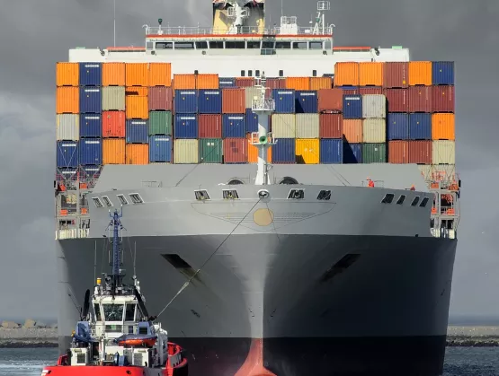
Tensions between the U.S. and China have reached fever pitch as the Trump administration imposed higher tariffs on $200 billion of Chinese goods last Monday, adding to the $50 billion in goods hit with higher duties earlier this year. Bloomberg News reported that “the combined $250 billion in products facing levies is almost half the value of imports from China last year.”China countered by meting out stiffer tariffs on $60 billion in U.S. goods, on top of the $50 billion already levied, and canceling planned trade negotiations with the Trump administration.Days before the sharp escalation of the trade conflict, SEMI president and CEO Ajit Manocha joined SEMI China president Lung Chu in hosting a closed-door round table with 16 senior semiconductor industry executives in Shanghai. The goal: An update from the China semiconductor sector on its needs as the chip industry braces to weather the conflict. Manocha and Chu then met with influential China media outlets including Semiconductor Manufacturing, China Integrated Circuit, Silicon Semiconductor and IC Café to reiterate SEMI’s position on trade.“The basic principles of SEMI are free and fair trade, open markets, cooperation for mutual benefit, and protection of intellectual property rights,” Manocha told the reporters. “Tariffs and trade frictions are bound to harm the industry’s development.”Manocha highlighted efforts over the past few months by the SEMI advocacy team to educate U.S. policymakers on the impact of tariffs on the development of the semiconductor industry. Last month, the office of the U.S. Trade Representative (USTR) held a hearing in Washington, D.C. to solicit public comment on then-proposed tariffs on $200 billion of Chinese imports to the U.S. Testifying on behalf of the semiconductor industry, SEMI stressed that tariffs on more than 100 tariff lines covering items critical to semiconductor manufacturing “will harm companies in the semiconductor supply chain by increasing business costs, introducing uncertainty, and stifling innovation.” SEMI had testified twice before this year – the first time in May, opposing levies on $34 billion in Chinese goods, and the second in July to speak out against higher duties on $16 billion worth of Chinese products.SEMI China president Lung Chu made clear the consensus of China’s semiconductor sector: The trade war will profoundly impact the global semiconductor industry. He also stressed that SEMI, as a global industry organization linking the global electronic semiconductor industry chain, will continue to promote win-win cooperation between the U.S. and China.Manocha reaffirmed SEMI’s longstanding commitment to promote cooperation among nations and policies that foster industry growth.“For the growth of the semiconductor industry, SEMI is focused on four important factors, and we call them the 4 T’s, namely Tax, Technology, Talent, Trade,” Manocha told the media. “All are indispensable for the development of the industry.” SEMI president and CEO Ajit Manocha and SEMI China president Lung Chu host press conference in Shanghai.Because the semiconductor industry is international, with key features spread across a number of regions, cross-border cooperation is an eternal theme, Chu told the gathering. To maintain the vitality of China's semiconductor industry, the region must deepen its integration with the international semiconductor ecosphere. He acknowledged that there will be no quick answers to easing trade tensions between the U.S. and China but that SEMI would continue to press ahead in efforts to help improve relations. Despite the conflict, the industry remains optimistic about the growth of China’s semiconductor industry, he said."However, we need to face up to the fact that there is still a certain gap between the domestic semiconductor industry and that of international advanced level,” Lu said. “Therefore, international cooperation is the key to industry growth."Of the four cornerstones of the semiconductor industry – design, manufacturing, testing and equipment materials – China in recent years has narrowed the gap with its international counterparts in testing capabilities, Chu said. For China’s semiconductor industry to flower, the region must build strengths in design, manufacturing and materials too.“The semiconductor industry needs long-term investment, persistence and patience, and also needs win-win cooperation, continuous innovation and product applications across the entire industry,” Chu said. “Money is not the only incentive.”Manocha emphasized the theme of international cooperation, with the global semiconductor industry working in harmony.“The global semiconductor industry chain is inseparable, and each region has its own advantages,” Manocha said. “So, we will continue to work hard to create a win-win, inclusive global industrial atmosphere.”For its part, SEMI China is focused on becoming the best partner for China to realize its semiconductor dream by continuing to provide services that encourage international cooperation. That role will grow in importance with SEMI’s expansion into application areas such as smart manufacturing, smart transportation, smart data and smart automotive – all requiring tighter integration of the electronics industry supply chain.Cherry Sun is a marketing manager at SEMI China.
Read More
Materials innovation has always been vital to the semiconductor industry. In the past, it was high-κ gate dielectrics. Today, Cobalt is seen as a replacement for Tungsten in middle-of-line (MOL) contacts.What materials innovation will the future bring?A likely answer is Graphene, the wonder material discovered in 2004.Graphene is one atomic layer of carbon, the thinnest and strongest material that has ever existed. It is 200 times stronger than steel and the lightest material known to man (1 square meter weighing around 0.77 mg). It is an excellent electrical and thermal conductor at room temperature with an electron mobility of ~ 200,000cm2.V-1.s-1. At one atomic layer, graphene is flexible and transparent. Other notable properties of Graphene are its uniform absorption of light across the visible and near infrared spectrum and its applicability towards spintronics-based devices.Graphene and Moore’s LawMoore’s Law scaling can be broken down into 4 key areas: Lithography FET Advanced Packaging (2.5D and 3D IC) Interconnect Material Solutions for upcoming nodes are starting to emerge in the first two areas (EUV and Nanowire- or Nanosheet-based FET respectively). Graphene play an important role in the latter two areas. For advanced packaging, Graphene can be used as a heat spreader (to lower overall thermal resistance), or as an EM shield (to lower crosstalk) as part of a 3D IC package.Active Graphene device layers can potentially be stacked on top of each other using a low-temperature transfer process ( 400°C) to allow for a dense heterogeneous “memory near compute” configuration. This is an area DARPA is actively researching as part of its new $1.5 billion Electronics Resurgence Initiative.Regarding interconnects, Copper interconnects are running out of steam and becoming a major IC bottleneck (projected 40% total delay for 7 nm node). Graphene’s high electron mobility and thermal conductivity make it an attractive interconnect material for MOL and back-end-of-line (BEOL), especially at line widths 30 nm.Graphene Device ApplicationsGraphene-based semiconductor applications are already starting to hit the market. A fully integrated optical transceiver (with a Graphene modulator and photodetector) operating at 25 Gb/s/channel was on display at the recent Mobile World Congress in Barcelona. San Diego-based Nanomedical Diagnostics is selling a medical device that uses a Graphene biosensor. Europe-based Emberion is building Graphene optoelectronic sensors that might find a home in LIDAR applications, where there is currently a focus on improving sensing in low-light conditions.What will the overall Graphene roadmap in the semiconductor industry look like? The history of ion implantation serves as a good example of how a fundamental scientific discovery moves from the lab to the foundry floor.The dominant view in the semiconductor industry at the time was that ion implantation would not work in practice (vs. thermal diffusion) and that, if it did, it would only marginally improve the manufacturing yields of existing products. There was nothing obvious about the transfer of ion bombardment techniques from nuclear physics research to semiconductor production.Varian (led by British physicist Peter Rose) built a new, advanced ion implant tool that Mostek (DRAM manufacturer based in Texas) was able to use to create MOS ICs with clear competitive advantages. The successful collaboration between Varian and Mostek was the turning point in the development of ion implantation as a major semiconductor manufacturing process. Over the next few years, semiconductor firms used ion implantation in a growing number of process steps and, by the late 1970s, it became one of the main processes used in semiconductor manufacturing.Likewise, the Graphene world needs to work closely with the semiconductor industry to develop the tools and techniques required to solve fundamental issues around Graphene growth (good uniformity over large area, low defect density) and Graphene transfer (high throughput, CMOS compatible). It is only then will we fully realize a future that includes 2D materials.The first step in this process is cross-industry education and initiating the dialogue between semiconductor industry and graphene companies. The National Graphene Association will be hosting the largest gathering of graphene companies and commercial stakeholders at the Global Graphene Expo Conference, October 15-17, 2018, in Austin, Texas.Learn more about graphene at the upcoming Global Graphene Expo Conference with dedicated panels of experts and investors, and roundtable discussions on how Graphene will impact the semiconductor industry. The event promo code is SEMINGA. About the AuthorAnand Chamarthy is the CEO and Co-Founder of Lab 91, an Austin-based startup that is working towards Graphene/CMOS integration at the foundry level. Anand can be reached at [email protected]. About the National Graphene AssociationThe National Graphene Association is the main organization and body in the U.S. promoting and advocating for commercialization of graphene and addressing critical issues such as standards and policy development.
Read More
SEMI Releases latest update to World Fab Forecast with adjusted semiconductor revenue consensus for second-half 2018 and 2019 Global semiconductor revenue in 2018 is now expected to reach $473.8 billion and clock a growth rate of 15 percent, a significant upward revision from the 7.5 percent expansion (to $442.9 billion) forecast at the start of the year by six research and investment forecasts tracked by SEMI Industry Research and Statistics (SEMI IR S). Data center growth will remain robust in the coming quarters, fueling demand for memory devices. In addition, cloud computing will continue to spur strong CPU, GPU, networking, ASIC, and DRAM and NAND demand through 2019, driving a consensus 3.63 percent year-to-year growth to reach the semiconductor revenue of $491 billion in 2019. Fab equipment spending (new and used) for 2018 is expected to increase by 14 percent to a record high of $63 billion, according to the last data from the SEMI World Fab Forecast, published by SEMI IR S. For 2019, fab equipment spending (new and used) is expected to increase 8 percent to another record of just under $68 billion. Memory continues to be the biggest swing factor in fab spending in 2018 and is expected to lead growth into 2020. 3D NAND will see the most capacity added in 2018 and 2019 with growth of 41 percent in 2018 and 27 percent in 2019, according to the SEMI World Fab Forecast. DRAM investment will see even stronger growth in 2018 and 2019 driven by new capacity addition as well as the continued technology shrink towards 1y/1z nm. For the first half of 2018, global spending for semiconductor fab equipment continues its growth momentum from 2017. Though we expect some softness in the second half of 2018, the outlook for 2019 remains robust with a fourth consecutive year of growth – the first such run since the 1990s. This prolonged growth cycle has been propelled by memory and will be extended by significant investment in China in 2019. Although a potential slowdown in 2020 is a concern, the overall outlook for semiconductor demand remains solid due to broad-based growth trends in data center, artificial intelligence (AI)/machine learning (ML), automotive, and industrial segments. Following are other SEMI forecasts for fab spending. Installed Capacity 3D NAND will see the most capacity added in both 2018 and 2019 with growth of 41 percent in 2018 and 27 percent in 2019. Foundry capacity growth is steady at 3 percent in 2018 and 6 percent in 2019, driven by both leading-edge and trailing-edge capacity buildup. 200mm fab capacity will increase 4 percent in 2018 and 3 percent in 2019, fueled by demand for MCU, sensors, PMIC, MOSFET and Driver IC. New Facilities / Construction Spending In 2018, there are 72 construction projects with investments totaling $15 billion, a year-over-year increase of 23 percent. Construction spending will reach all-time highs with China continuing its lead at US$7 billion in 2018, shattering its own record of $6.3 billion investment in 2017. Most construction spending in 2018 will be for Memory (just under $9 billion), primarily for 3D NAND followed by DRAM. Foundry will log second place in construction spending at just under $5 billion. Fab Equipment Spending Fab equipment spending (new and used) for 2018 is expected to jump 14 percent to a record high of US$63 billion, flat from the forecast issued in June 2018. Equipment spending (new and used) for 2019 is expected to increase 8 percent to another record of just under US$68 billion, a downward adjustment from +9 percent published in June 2018. We believe equipment spending will remain healthy, driven by solid, broad-based demand and predictable technology investments on top of constructive SEMICAP equipment fundamentals. Activity Report The August report features 1,265 records including about 300 Opto- and LED-related facilities. We have made 223 changes related to 216 fabs/lines. The modifications include the addition of new records, changes to existing records, the deletion of records since the February 2018 World Fab Forecast report. We are tracking 103 future facilities/lines with various probabilities that will start volume production in 2018 or later. Download a sample report Not a subscriber? Please review SEMI fab databases listed below. Our databases deliver the latest forecast and a complete analysis of front-end fabs and foundries worldwide. They are ideal resources to empower your market research. Eugenia Liu is a Senior Product Marketing Manager at SEMI.
Read More