downloadGroupGroupnoun_press release_995423_000000 copyGroupnoun_Feed_96767_000000Group 19noun_pictures_1817522_000000Member company iconResource item iconStore item iconGroup 19Group 19noun_Photo_2085192_000000 Copynoun_presentation_2096081_000000Group 19Group Copy 7noun_webinar_692730_000000Path
Skip to main content
Default Banner Image

United States

MILPITAS, Calif. — November 3, 2021 — SEMICON West, North America’s premier microelectronics exhibition and conference that unites players across the entire electronics manufacturing and design supply chain, and FLEX Conference, the annual event focused on flexible hybrid and printed electronics innovations, will co-locate at the Moscone Center in San Francisco, July 11-14, 2022. Registration for both events will open next spring.

SEMI Event Logo“Flexible hybrid electronics (FHE) technologies are key drivers of digital transformation as they advance to enable smart transportation, buildings and infrastructure, equipment sensorization, and wearable and conformable medical devices,” said Dr. Melissa Grupen-Shemansky, SEMI CTO and vice president of SEMI Technology Communities. “Next year’s co-location of SEMICON West 2022 and FLEX Conference 2022 will gather microelectronics and FHE leaders to explore new innovation opportunities across both industries as they work together to advance system-level products through critical technologies such as heterogeneous integration.”

“With collaboration the fuel of microelectronics innovation, the co-location of SEMICON West 2022 and FLEX Conference 2022 promises to uncover new ways for semiconductor and FHE leaders to accelerate global digitization in ways that continue to improve how we work and live,” said David Anderson, president of SEMI Americas.

FLEX Conference, in its 20th year, showcases innovations emerging from public-private partnerships formed by SEMI Technology Communities SEMI-FlexTech, SEMI-NBMC (Nano-Bio Materials Consortium) and SEMI-NextFlex. At FLEX Conference 2022, keynotes, panels discussions, technical sessions, and product-based TechTALKS will highlight the latest advances in flexible and printed electronics, including applications that deepen interactions between users and their surroundings. The event will focus on equipment, processes, materials and applications driving the latest technology breakthroughs and how they help shape business strategy.

The Design Automation Conference (DAC), the largest meeting in the electronic design automation (EDA) industry, will also co-locate with SEMICON West 2022. Registration will open in the spring of 2022.

About SEMI

SEMI® connects more than 2,400 member companies and 1.3 million professionals worldwide to advance the technology and business of electronics design and manufacturing. SEMI members are responsible for the innovations in materials, design, equipment, software, devices, and services that enable smarter, faster, more powerful, and more affordable electronic products. Electronic System Design Alliance (ESD Alliance), FlexTech, the Fab Owners Alliance (FOA), MEMS & Sensors Industry Group (MSIG) and the SOI Consortium, are SEMI Strategic Technology Communities, defined groups within SEMI focused on specific technologies. Visit www.semi.org to learn more, contact one of our worldwide offices, and connect with SEMI on LinkedIn and Twitter.

Association Contact   

Scott Stevens, Cardinal Communications for SEMI Americas

Phone: 1.512.288.4050 

Email: [email protected]

MILPITAS, Calif. ─ November 4, 2021 ─ Worldwide silicon wafer shipments increased 3.3% to 3,649 million square inches in the third quarter of 2021 compared to the previous quarter, a new industry record, the SEMI Silicon Manufacturers Group (SMG) reported in its quarterly analysis of the silicon wafer industry. Third-quarter 2021 silicon wafer shipments grew 16.4% from the 3,135 million square inches recorded during the same quarter last year.

SEMI logo“Silicon wafer shipments reached a new high in third quarter, with higher shipments in all diameters, which support the large variety of semiconductor devices needed for the modern economy,” said Neil Weaver, Chairman of SEMI SMG and Vice President of Product Development and Applications Engineering at Shin Etsu Handotai America. “Silicon wafer demand is expected to remain high, as many new fabs will ramp up in the next several years.”
 

Silicon Area Shipment Trends – Semiconductor Applications Only


                                                                       Millions of Square Inches


2Q 2020

3Q 2020

4Q 2020

1Q 2021

2Q 2021

3Q 2021

Total

3,152

3,135

3,200

3,337

3,534

3,649

Source: SEMI (www.semi.org), November 2021


Data cited in this release include polished silicon wafers such as virgin test and epitaxial silicon wafers, as well as non-polished silicon wafers shipped to end users.

Silicon wafers are the fundamental building material for the majority of semiconductors, which are vital components of all electronics including computers, telecommunications products, and consumer devices. The highly engineered thin disks are produced in diameters of up to 12 inches and serve as the substrate material on which most semiconductor devices, or chips, are fabricated.

The SMG is a sub-committee of the SEMI Electronic Materials Group (EMG) and is open to SEMI members involved in manufacturing polycrystalline silicon, monocrystalline silicon or silicon wafers (e.g., as cut, polished, epi). The SMG facilitates collective efforts on issues related to the silicon industry including the development of market information and statistics about the silicon industry and the semiconductor market.

For more information, please visit SEMI Worldwide Silicon Wafer Shipment Statistics.

About SEMI

SEMI® connects more than 2,400 member companies and 1.3 million professionals worldwide to advance the technology and business of electronics design and manufacturing. SEMI members are responsible for the innovations in materials, design, equipment, software, devices, and services that enable smarter, faster, more powerful, and more affordable electronic products. Electronic System Design Alliance (ESD Alliance), FlexTech, the Fab Owners Alliance (FOA) and the MEMS & Sensors Industry Group (MSIG) are SEMI Strategic Association Partners, defined communities within SEMI focused on specific technologies. Visit www.semi.org to learn more, contact one of our worldwide offices, and connect with SEMI on LinkedIn and Twitter.

Association Contact

Michael Hall/SEMI
Phone: 1.408.943.7988
Email: [email protected]

MILPITAS, Calif. – October 28, 2021 – SEMI, the industry association serving the global electronics design and manufacturing supply chain, today applauded the inclusion of an Advanced Manufacturing Investment Credit in the Build Back Better reconciliation bill. A minimum credit of 5%, increasing to 25% if certain conditions are met, would be provided for buildings and equipment to manufacture semiconductors and semiconductor tooling equipment if the facility commences construction before January 1, 2027.

SEMI logo“SEMI is thrilled that a semiconductor manufacturing tax credit for the production of chips and semiconductor tools has been included in the Build Back Better reconciliation bill,” said Ajit Manocha, SEMI president and CEO. “This credit will provide a strong incentive for the production of semiconductors and semiconductor manufacturing equipment in the United States and make the U.S. more competitive in this vital industry. We thank President Joe Biden, Senate Finance Committee Chairman Ron Wyden for his leadership and determination to include this provision, and the original co-sponsors of the FABS Act.”

“We look forward to working with Congress to pass this bill and fund the CHIPS Act programs, which together will further strengthen the semiconductor supply chain in the United States, help U.S. policies keep pace with incentive proposals around the world and create thousands of high-skill jobs,” Manocha said. “The inclusion of semiconductor tool manufacturing facilities is particularly important, as lead times and demand for new tools continue to grow. In addition, the delayed requirement to amortize research expenses and the maintenance of the Foreign-Derived Intangible Income deduction are other important elements that will preserve and improve the competitiveness of the industry in the United States.”

The Advanced Manufacturing Investment Credit is a modified, temporary version of the Facilitating American-Built Semiconductors (FABS) Act (S.2107). The credit included in the reconciliation bill retains important features of the FABS Act credit, including an election to receive the tax credit as a direct payment, for investments in semiconductor manufacturing facilities and facilities and equipment to produce semiconductor manufacturing tools.

Visit SEMI Global Advocacy to learn more about public policy efforts and developments, and SEMI Workforce Development for more information on efforts to address the microelectronics industry’s talent needs.


About SEMI

SEMI® connects more than 2,400 member companies and 1.3 million professionals worldwide to advance the technology and business of electronics design and manufacturing. SEMI members are responsible for the innovations in materials, design, equipment, software, devices, and services that enable smarter, faster, more powerful, and more affordable electronic products. Electronic System Design Alliance (ESD Alliance), FlexTech, the Fab Owners Alliance (FOA) and the MEMS & Sensors Industry Group (MSIG) are SEMI Strategic Technology Communities, defined communities within SEMI focused on specific technologies. Visit www.semi.org to learn more, contact one of our worldwide offices, and connect with SEMI on LinkedIn and Twitter.


SEMI Contact

Samer Bahou/SEMI

Phone: 1.408.943.7870

Email: [email protected]

MILPITAS, Calif. — October 21, 2021 — North America-based semiconductor equipment manufacturers posted $3.72 billion in billings worldwide in September 2021 (three-month moving average basis), according to the September Equipment Market Data Subscription (EMDS) Billings Report published today by SEMI. The billings figure is 1.7% higher than final August 2021 billings of $3.66 billion and 35.5% higher than September 2020 billings of $2.74 billion.

SEMI logo“Monthly billings of North America-based semiconductor equipment manufacturers edged up in September to near the record high set in July,” said Ajit Manocha, president and CEO of SEMI “The ongoing growth in key end-market segments and silicon content continues to drive gains for the semiconductor manufacturing ecosystem including equipment.”

The SEMI Billings report uses three-month moving averages of worldwide billings for North American-based semiconductor equipment manufacturers. Billings figures are in millions of U.S. dollars.


Billings
(3-mo. Avg.)

Year-Over-Year

April 2021

$3,428.9

50.3%

May 2021

$3,588.5

53.1%

June 2021

$3,690.2

59.2%

July 2021

$3,857.4

49.8%

August 2021 (final)

$3,656.3

37.8%

September 2021 (prelim)

$3,718.1

35.5%

Source: SEMI (www.semi.org), October 2021


SEMI publishes a monthly North American Billings report and issues the Worldwide Semiconductor Equipment Market Statistics (WWSEMS) report in collaboration with the Semiconductor Equipment Association of Japan (SEAJ). The WWSEMS report currently reports billings by 24 equipment segments and by seven end market regions. SEMI also has a long history of tracking semiconductor industry fab investments in detail on a company-by-company and fab-by-fab basis in its World Fab Forecast and SEMI FabView databases. These powerful tools provide access to spending forecasts, capacity ramp, technology transitions, and other information for over 1,000 fabs worldwide. For an overview of available SEMI market data, please visit www.semi.org/en/MarketInfo.

The data contained in this release were compiled by David Powell, Inc., an independent financial services firm, without audit, from data submitted directly by the participants. SEMI and David Powell, Inc. assume no responsibility for the accuracy of the underlying data.


About SEMI

SEMI® connects more than 2,400 member companies and 1.3 million professionals worldwide to advance the technology and business of electronics design and manufacturing. SEMI members are responsible for the innovations in materials, design, equipment, software, devices, and services that enable smarter, faster, more powerful, and more affordable electronic products. Electronic System Design Alliance (ESD Alliance), FlexTech, the Fab Owners Alliance (FOA) and the MEMS & Sensors Industry Group (MSIG) are SEMI Strategic Technology Communities, defined communities within SEMI focused on specific technologies. Visit www.semi.org to learn more, contact one of our worldwide offices, and connect with SEMI on LinkedIn and Twitter.

Association Contact

Michael Hall/SEMI
Phone: 1.408.943.7988
Email: [email protected]


Notes

Next SEMI Billings report is November 22, 2021 at 3:00pm Pacific.

For information on SEAJ Billings Express Report, visit www.seaj.or.jp. 

MUNICH, Germany ─ October 19, 2021 ─ With leading-edge technologies such as artificial intelligence (AI), 5G and robotics at the heart of digital transformation, SEMICON Europa 2021 will convene industry visionaries and experts 16-19 November for insights into the latest innovations and smart applications powering the next wave of semiconductor industry growth. Europe’s premier event connecting the entire electronics design and manufacturing supply chain, SEMICON Europa, co-located with productronica, returns to Messe München, in Munich, Germany for a live exhibition and conferences. Registration is open.

SEMICON Europa logoSemiconductor manufacturing resiliency is growing in importance as the semiconductor supply chain works to overcome disruptions and shortages trigged by the pandemic. SEMICON Europa will explore ways the global supply chain can better withstand shocks in the future. 

“We are excited to welcome back key semiconductor industry players in person in Munich,” said Laith Altimime, president of SEMI Europe. “SEMICON Europa gathers experts across the value chain for the collaboration and innovation critical to Europe’s semiconductor industry growth. Visitors will take a deep dive into how semiconductors are making manufacturing, automotive and healthcare smarter to drive higher efficiency and productivity across a wide range of applications.”

SEMICON Europa 2021 will examine how the semiconductor industry can integrate environmental and social sustainability into its growth strategy to help transform Europe into a sustainable, connected digital hub that enables life-changing applications for current and future generations. The event will also highlight process, materials and technology innovations that make it possible for chipmakers to implement cutting-edge 3D packaging for a broad range of new application-specific technologies.

SEMICON Europa Highlights

  • Executive Forum (New!): European Ecosystems Connecting the Digital Future – 16 November. Presenting organizations: Bosch, Cariad, Edwards Vacuum, European Commission, Fraunhofer EMFT, imec, Intel, Infineon, KLA, CEA-Leti, Merck KGaA, Darmstadt, Germany, NXP Semiconductors, Philips, Samsung, TSMC
  • 25th Fab Management Forum: Expanding European Manufacturing Footprint –17 November
  • Advanced Packaging Conference: Material and Process Challenges in the Era of Digital Transformation – 18 November

Smart Technologies and EU-funded Projects

The new TechARENA in Hall B1 at SEMICON Europa 2021 will feature smart technologies and showcase how semiconductors are enabling technology innovation and solutions to global challenges. Focus topics will be manufacturing, mobility, medical, the future of computing, telecommunications, and workforce development.

The EU Digital Lounge in Hall B1 will provide updates on EU-funded semiconductor projects including the following:

  • MicroElectronics Training, Industry and Skills (METIS)
  • European Cooperation platform of Vocational Excellence in Microelectronics (ECoVEM)
  • Metrology Advances for Digitized Electronics Components and Systems Industry 4.0 (MADEin4)
  • Edge-to-Cloud Intelligence for Resilient Manufacturing (the IMOCO4.E Initiative)

Visit SEMICON Europa programs and conferences for additional details.

SEMICON Europa Premier Sponsors

  • Platinum: Samsung, Tokyo Electron Europe
  • Gold: JCET
  • Silver: Bosch, Evatec, KLA, SCREEN
  • Event sponsors: AP&S, ASE Group, Atotech, DAS Environmental Expert, DB Schenker, DISCO, EBARA, Edwards Vacuum, Flexciton, INFICON, InnoLas Photonics, Merck KGaA, Darmstadt, Germany, Pfeiffer Vacuum, Siconnex Customized Solutions, VAT, YES, ZEISS

For more details, please visit the SEMICON Europa 2021 website and connect with SEMI Europe on Twitter or LinkedIn @SEMIEurope (#SEMICONEuropa).

About SEMI

SEMI® connects more than 2,400 member companies and 1.3 million professionals worldwide to advance the technology and business of electronics design and manufacturing. SEMI members are responsible for the innovations in materials, design, equipment, software, devices, and services that enable smarter, faster, more powerful, and more affordable electronic products. Electronic System Design Alliance (ESD Alliance), FlexTech, the Fab Owners Alliance (FOA) and the MEMS & Sensors Industry Group (MSIG) are SEMI Strategic Technology Communities, defined communities within SEMI focused on specific technologies. Visit www.semi.org to learn more, contact one of our worldwide offices, and connect with SEMI on LinkedIn and Twitter.

Association Contact

Serena Brischetto / SEMI Europe
Phone: +49 30 3030 8077-11
Email: [email protected]

SEMICON Japan 2021 Returns Live in Tokyo to Highlight Semiconductor Industry Innovation, Growth Opportunities

TOKYOOctober 19, 2021 – Leading-edge technologies including artificial intelligence (AI), 5G, Internet of Things (IoT), MEMS and sensors, quantum computing and advanced 3D packaging will take center stage at SEMICON Japan 2021 Hybrid as visionary keynote speakers and industry leaders gather December 15-17 to share insights into the latest trends and innovations driving semiconductor industry growth. The largest and most influential exhibition in Japan for electronics manufacturing, SEMICON Japan returns to Tokyo Big Sight with a full-scale, in-person exposition and conferences combined with online access. Registration is open for exhibits and all programs.

SEMICON Japan Hybrid logoThemed Forward as One, SEMICON Japan 2021 Hybrid will showcase opportunities for the semiconductor manufacturing and design supply chain to enable a smarter world through advances in Smart Mobility, mobile communications and other applications powering industry growth. The rising importance of semiconductor manufacturing sustainabilty will also come into sharp focus as more companies across the supply chain work to reduce their carbon footprint.  

With Japan producing more than 40% of the equipment and materials for global semiconductor manufacturing, SEMICON Japan is a critical source for the latest technology and business developments from key suppliers.

Industry Visionaries Presenting at SEMICON Japan 2021

Intel headshot

Peng Bai, Corporate Vice President, Manufacturing, Supply Chain and Operations General Manager, Global Sourcing for Equipment and Materials, Intel 

Keynote

Intel logo
TSMC headshot

Chris Chern, Advanced Packaging Development: 3DIC RD Center in Japan, TSMC 

Advanced Packaging Development: TSMC 3DIC RD Center in Japan

TSMC logo


Dell headshot

Lawrence Vivolo, Senior Business Development Manager, Automotive & Semiconductor Design, Unstructured Data Solutions, Dell Technologies

A Revolution in Smart Factories is Coming. Are You Ready?

100


Applied Materials headshot

Prabu Raja, Senior Vice President, Semiconductor Products Group, Applied Materials

PPACt™ Scaling in the AI Era: A New Way Forward for the Semiconductor Industry

Applied Materials logo


IBS headshot

Handel Jones, CEO, International Business Strategies

Opportunities and Challenges for Electronics, Semiconductors, and AI in China, and Perspective on 2025 and 2030

IBS logo


SEMICON Japan 2021 Sponsors

  • Platinum sponsors include Disco Corporation, Hightec Systems Corporation, Hitachi High-Tech Corporation, Screen Semiconductor Solutions Co., Ltd., and Tokyo Electron Limited.
  • Gold sponsors include Advantest, Applied Materials, Ebara, JSR, Kokusai Electric, Lam Research, Nikon, and Tokyo Seimitsu.

Learn more at SEMICON Japan 2021 Hybrid.

About SEMI

SEMI® connects more than 2,400 member companies and 1.3 million professionals worldwide to advance the technology and business of electronics design and manufacturing. SEMI members are responsible for the innovations in materials, design, equipment, software, devices, and services that enable smarter, faster, more powerful, and more affordable electronic products. Electronic System Design Alliance (ESD Alliance), FlexTech, the Fab Owners Alliance (FOA) and the MEMS & Sensors Industry Group (MSIG) are SEMI Strategic Technology Communities, defined communities within SEMI focused on specific technologies. Visit www.semi.org to learn more, contact one of our worldwide offices, and connect with SEMI on LinkedIn and Twitter.

Association Contact

Hiroki Yomogita, Marketing Director, SEMI Japan

Phone: 81.3.3222.5755

Email: [email protected]

MILPITAS, Calif. ─ October 18, 2021 ─ Global silicon wafer shipments are projected to register robust growth through 2024, with wafer area increasing 13.9% year-over-year in 2021 to a record high of nearly 14,000 millions of square inches (MSI), SEMI reported today in its annual silicon shipments forecast for the semiconductor industry. The logic, foundry and memory sectors are contributing to the 2021 silicon shipment expansion.

SEMI logo“We are seeing a significant increase in silicon shipments driven by strong secular demand for semiconductors across multiple end markets,” said Inna Skvortsova, an Industry Research & Statistics market analyst at SEMI. “The growth momentum is expected to continue in the following years but could be tempered by the slowing pace of the macroeconomic recovery and timing of the wafer manufacturing capacity additions needed to meet growing demand.”

2021 Silicon* Shipment Forecast (MSI)


Actual

Forecast


2019

2020

2021

2022

2023

2024

MSI

11,677

12,290

13,998

14,896

15,587

16,037

Annual Growth

-6.9%

5.3%

13.9%

6.4%

4.6%

2.9%

*Total Electronic Grade Silicon Disks – Excludes Non-Polished and Reclaimed Wafers

*Shipments are for semiconductor applications only and do not include solar applications

Source: SEMI (www.semi.org), October 2021


Silicon wafers are the fundamental building material for the majority of semiconductors, which are vital components of all electronics including computers, telecommunications products, and consumer devices. The highly engineered thin disks are produced in diameters of up to 12 inches and serve as the substrate material on which most semiconductor devices, or chips, are fabricated.

All data cited in this release is inclusive of polished silicon wafers and epitaxial silicon wafers shipped by wafer manufacturers to end users. The data does not include non-polished or reclaimed wafers.

For more information, please visit SEMI Worldwide Silicon Wafer Shipment Statistics.

About SEMI

SEMI® connects more than 2,400 member companies and 1.3 million professionals worldwide to advance the technology and business of electronics design and manufacturing. SEMI members are responsible for the innovations in materials, design, equipment, software, devices, and services that enable smarter, faster, more powerful, and more affordable electronic products. Electronic System Design Alliance (ESD Alliance), FlexTech, the Fab Owners Alliance (FOA) and the MEMS & Sensors Industry Group (MSIG) are SEMI Strategic Association Partners, defined communities within SEMI focused on specific technologies. Visit www.semi.org to learn more, contact one of our worldwide offices, and connect with SEMI on LinkedIn and Twitter.

Association Contact

Michael Hall/SEMI
Phone: 1.408.943.7988
Email: [email protected]

MILPITAS, Calif. October 12, 2021 — Electronic System Design (ESD) industry revenue increased 14.6% year-over-year from $2,783.9 million to $3,191.4 million in Q2 2021, the ESD Alliance, a SEMI Technology Community, announced today in the latest Electronic Design Market Data (EDMD) report. The four-quarter moving average, which compares the most recent four quarters to the prior four, rose 15.5%, the highest annual growth since 2011.   

SEMI ESDA logo“The industry reported double-digit year-over-year revenue growth for Q2 2021,” said Walden C. Rhines, Executive Sponsor, SEMI Electronic Design Market Data report. “Product categories Computer Aided Engineering (CAE), Printed Circuit Board and Multi-Chip Module (PCB and MCM), Semiconductor IP (SIP), and Services all reported double-digit growth.”

“Geographically, all regions reported growth on a rolling four-quarter basis, with the Americas; Asia Pacific (APAC); and Europe, Middle East, and Africa (EMEA) showing a substantial year-over-year increase,” Rhines added.

The companies tracked in the EDMD report employed 49,964 people globally in Q2 2021, a 7.3% increase over the Q2 2020 headcount of 46,579 and up 1.9% compared to Q1 2021.

The quarterly EDMD report contains detailed revenue information with the following category and geographic breakdowns.


Revenue by Product and Application Category – Year-Over-Year Change

  • CAE revenue increased 10.1% to $1,014.6 million. The four-quarter CAE moving average increased 11%.
  • IC Physical Design and Verification revenue decreased 0.4% to $581.5 million. The four-quarter moving average for the category rose 18.6%.
  • Printed Circuit Board and Multi-Chip Module (PCB and MCM) revenue increased 16.8% to $284.4 million. The four-quarter moving average for PCB and MCM increased 9.4%.
  • SIP revenue rose 27.1% to $1,204.9 million. The four-quarter SIP moving average grew 20.5%.
  • Services revenue increased 23.1% to $106.1 million. The four-quarter Services moving average increased 8.8%.


Revenue by Region – Year-Over-Year Change

  • The Americas, the largest reporting region by revenue, purchased $1,367.3 million of electronic system design products and services in Q2 2021, an 18.3% increase. The four-quarter moving average for the Americas rose 15.2%.
  • Europe, Middle East and Africa revenue increased 9.9% to $415 million. The four-quarter moving average for EMEA grew 7.8%.
  • Japan revenue decreased 1% to $237.9 million. The four-quarter moving average for Japan rose 1.9%.
  • Asia Pacific revenue increased 15.9% to $1,171.2 million. The four-quarter moving average for APAC increased 22.9%.


About the EDMD Report

The ESD Alliance Electronic Design Market Data (formerly the Market Statistics Service) report presents EDA, SIP and services industry revenue data quarterly. Both public and private companies contribute data to the report available from SEMI. Each quarterly report is published approximately three months after quarter close. EDMD report data is segmented as follows:

  • Revenue by product category (CAE, IC Physical Design and Verification, Semiconductor IP, PCB/MCM Layout, and Services) including numerous detailed sub-categories
  • Revenue by geographic region (Americas, EMEA, Japan and APAC)
  • Total employment at participating companies

For information about SEMI market research reports, visit the SEMI Market Research Reports and Databases Catalog.


About the Electronic System Design Alliance

The Electronic System Design (ESD) Alliance, a SEMI Technology Community, is the central voice to communicate and promote the value of the semiconductor design ecosystem as a vital component of the global electronics industry. As an international association of companies providing goods and services throughout the semiconductor design ecosystem, it is a forum to address technical, marketing, economic and legislative issues affecting the entire industry. For more information about the ESD Alliance, visit http://esd-alliance.org.


About SEMI

SEMI® connects more than 2,400 member companies and 1.3 million professionals worldwide to advance the technology and business of electronics design and manufacturing. SEMI members are responsible for the innovations in materials, design, equipment, software, devices, and services that enable smarter, faster, more powerful, and more affordable electronic products. Electronic System Design Alliance (ESD Alliance), FlexTech, the Fab Owners Alliance (FOA) and the MEMS & Sensors Industry Group (MSIG) are SEMI Strategic Association Partners, defined communities within SEMI focused on specific technologies. Visit www.semi.org to learn more, contact one of our worldwide offices, and connect with SEMI on LinkedIn and Twitter.

The information supplied by the ESD Alliance is believed to be accurate and reliable, but the ESD Alliance assumes no responsibility for any errors that may appear in this document. All trademarks and registered trademarks are the property of their respective owners.


Press Contacts                                                                                 

Paul Cohen

ESD Alliance

A SEMI Technology Community

978-769-2106             
 

Jack Taylor

Siemens EDA

512-560-7143 

MILPITAS, Calif. — October 12, 2021 — Fueled by pent-up demand for automotive electronics caused by semiconductor supply chain disruptions wrought by the pandemic, worldwide installed capacity for power and compound semiconductor fabs is projected to top 10 million wafers per month (WPM) for the first time in 2023, growing to 10.24 million WPM (in 200mm equivalents) and climbing to 10.6 million WPM in 2024, SEMI announced today in its Power & Compound Fab Report to 2024.

SEMI logo
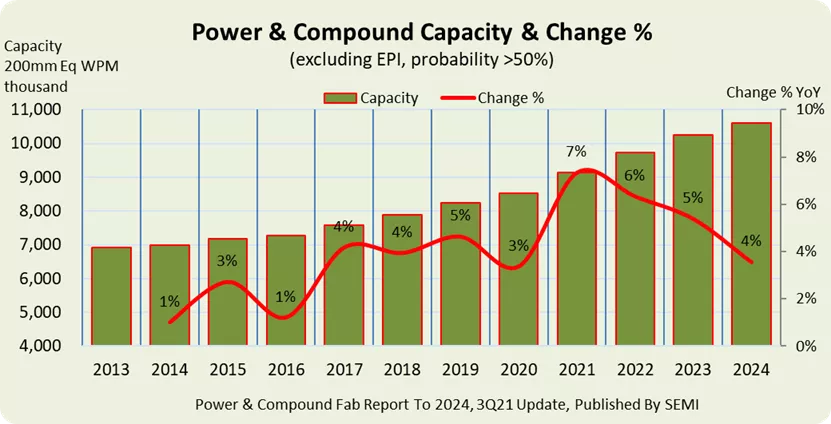
China is expected to claim the largest share of installed capacity – 33% – by 2023, followed by Japan at 17%, Europe and the Mideast at 16%, and Taiwan at 11%, proportions that are expected to change little as the industry remains on track to add more than 360,000 WPM in 2024.

The SEMI Power & Compound Fab Report to 2024 reveals that 63 companies are expected to add more than 2 million WPM (in 200mm equivalents) from 2021 through 2024. Infineon, Hua Hong Semiconductor, STMicroelectronics and Silan Microelectronics will lead the way, together adding a projected 700,000 WPM.   


Power Compound Chart


Installed capacity for the power and compound fab industry grew 5% year-over-year (YOY) in 2019 and 3% in 2020 before surging 7% in 2021. YOY growth is projected to remain strong at 6% in 2022 and 5% in 2023 as the industry tops the 10 million WPM mark.

The industry is also adding production facilities. From 2021 through 2024, 47 high-probability facilities and lines (R&D to high volume, including epitaxial wafers) are expected to go online to bring the industry total to 755, a number that could be eclipsed if new facilities and lines are announced. 

The SEMI Power & Compound Fab Report to 2024 covers 957 facilities and lines operational over the 12 years from 2013 to 2024, including facilities that are or will be closed, and new facilities starting operation.

For more information about the report or to download sample data, please visit Power & Compound Fab Report to 2024.


About SEMI

SEMI® connects more than 2,400 member companies and 1.3 million professionals worldwide to advance the technology and business of electronics design and manufacturing. SEMI members are responsible for the innovations in materials, design, equipment, software, devices, and services that enable smarter, faster, more powerful, and more affordable electronic products. Electronic System Design Alliance (ESD Alliance), FlexTech, the Fab Owners Alliance (FOA) and the MEMS & Sensors Industry Group (MSIG) are SEMI Strategic Association Partners, defined communities within SEMI focused on specific technologies. Visit www.semi.org to learn more, contact one of our worldwide offices, and connect with SEMI on LinkedIn and Twitter.


Association Contacts

Michael Hall/SEMI
Phone: 1.408.943.7988
Email: [email protected]

Christian G. Dieseldorff/SEMI
Phone: 1.408.943.7940
Email: [email protected]