downloadGroupGroupnoun_press release_995423_000000 copyGroupnoun_Feed_96767_000000Group 19noun_pictures_1817522_000000Member company iconResource item iconStore item iconGroup 19Group 19noun_Photo_2085192_000000 Copynoun_presentation_2096081_000000Group 19Group Copy 7noun_webinar_692730_000000Path
Skip to main content
Default Banner Image

Taiwan

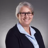
Don Foldenauer Joins YES as Vice President of Operations

FREMONT, Calif. – July 19, 2021 — YES (Yield Engineering Systems, Inc.), a leading manufacturer of process equipment for semiconductor advanced packaging, life sciences and “More-than-Moore” applications, today announced that Don Foldenauer is the company’s new VP of Operations.

“I am very pleased to welcome Don to our executive staff,” said Vinod Mahendroo, Senior VP of Operations at YES. “I expect that his extensive industry experience and proven track record of building and managing high-functioning teams will be considerable assets to YES as we continue our rapid growth and transition to a world-class, global manufacturer.”

Mr. Foldenauer began his career as a design engineer of semiconductor manufacturing equipment systems and has been awarded multiple patents. He spent more than 15 years in Field Operations management at Applied Materials and KLA-Tencor. His resumé also includes over 15 years in Manufacturing Operations management at Applied Materials, followed by VP of Operations roles at three contract manufacturers: Jabil, Celestica, and Ultra Clean Technology. In addition to holding bachelor’s degrees in electronic engineering and business management, and an MBA from San Jose State University, he is a regular guest lecturer at Stanford University on the topics of photovoltaics and semiconductor manufacturing.

About YES
YES (Yield Engineering Systems, Inc.) is a preferred provider of high-tech, cost-effective equipment for transforming surfaces, materials and interfaces. The company’s product lines include vacuum cure systems, chemical vapor deposition (CVD) systems, and plasma etching tools used for precise surface modification and thin-film coating of semiconductor wafers, semiconductor and MEMS devices, biosensors and medical substrates. With YES, customers ranging from startups to Fortune 100 companies can create and volume-produce products in a wide range of markets, including Advanced Packaging, MEMS, Augmented Reality/Virtual Reality and Life Sciences. YES is headquartered in Fremont, California, with a growing presence globally. For more information, please visit www.yieldengineering.com.

ESPOO, Finland, 28th of July 2021 – Picosun Group delivers cutting-edge Atomic Layer Deposition (ALD) technology to ams OSRAM for volume manufacturing of optical semiconductor devices.

ams OSRAM has invested in a fully automated PICOSUN® Morpher production cluster, which can deposit multiple materials on a batch of wafers even during the same process run. The flexibility and process variety of the PICOSUN® Morpher system is a key advantage, which enables volume production as well as the testing of new processes for R&D of future products.

Picosun Group and ams OSRAM have collaborated in a public funded project FLINGO (m-era.net project) to develop new ALD materials and processes to improve the characteristics of LEDs, such as efficiency and durability. The collaboration between the parties will continue after the ALD system delivery with activities to further expand the use of ALD in optoelectronic semiconductor processing.

“We have been working with Picosun since 2010 and now with this investment we can bring our collaboration to the next level. We are very excited to have the PICOSUN™ Morpher F cluster platform installed in our cleanroom”, states Dr. Sebastian Taeger, at ams OSRAM.

“The optical semiconductor market is one focus area of Picosun today. It is a fast-growing market where we have a strong presence with our tailored solutions for compound semiconductor-based devices. We have had excellent collaboration with the ams OSRAM technical team during project FLINGO and during the system specification stage. The expertise from both companies has resulted in optimized ALD solutions to boost the performance of the customer’s products.”, continues Dr. Christoph Hossbach, General Manager of Picosun Europe GmbH.

More information:
Dr. Christoph Hossbach, General Manager, Picosun Europe GmbH
Tel. +49 1522 449 49 11
Email: [email protected]
www.picosun.com

Picosun provides the most advanced AGILE ALD® (Atomic Layer Deposition) thin film coating solutions for global industries. Picosun’s ALD solutions enable technological leap into the future, with turn-key production processes and unmatched, pioneering expertise in the field – dating back to the invention of the technology itself. Today, PICOSUN® ALD equipment are in daily manufacturing use in numerous leading industries around the world. Picosun is based in Finland, with subsidiaries in Germany, USA, Singapore, Japan, South Korea, China mainland and Taiwan, offices in India and France, and a world-wide sales and support network. Visit www.picosun.com.

About ams OSRAM
The ams-OSRAM Group, including the listed companies ams AG as parent company and OSRAM Licht AG, is a global leader in optical solutions. By adding intelligence to light and passion to innovation, we enrich people’s lives. This is what we mean by Sensing is Life.

With over 110 years of combined history, our core is defined by imagination, deep engineering expertise and the ability to provide global industrial capacity in sensor and light technologies. We create exciting innovations that enable our customers in the consumer, automotive, healthcare and industrial sectors maintain their competitive edge. We thereby drive innovation that meaningfully improves the quality of life in terms of health, safety and convenience, while reducing impact on the environment.
Our around 30,000 employees worldwide focus on innovation across sensing, illumination and visualization to make journeys safer, medical diagnosis more accurate and daily moments in communication a richer experience. Our work creates technology for breakthrough applications, which is reflected in over 15,000 patents granted and applied. Headquartered in Premstaetten/Graz (Austria) with a co-headquarter in Munich (Germany), the group achieved well over USD 5 billion combined revenues in 2020 (pro-forma).

ams AG is a listed company on the SIX Swiss Exchange (ISIN: AT0000A18XM4). OSRAM Licht AG remains a listed company on the XETRA market in Germany (ISIN: DE000LED4000).

To find out more about us on https://ams-osram.com

ams is a registered trademark of ams AG. In addition many of our products and services are registered or filed trademarks of ams Group. All other company or product names mentioned herein may be trademarks or registered trademarks of their respective owners. Information provided in this press release is accurate at time of publication and is subject to change without advance notice.
Join ams social media channels: >Twitter >LinkedIn >Facebook >YouTube
Join OSRAM social media channels: >Twitter >LinkedIn >Facebook >YouTube

Please note: The ams brand is owned by ams AG, the OSRAM brand is owned by OSRAM GmbH. ams group and OSRAM group are in the process of integration. The combination of the ams and OSRAM brand is not representing a new brand. This is a visual symbol of the two companies coming together, representing the aspiration of our future joined group.


ClassOne Technology (classone.com), global provider of advanced semiconductor electroplating and surface preparation systems, announced that it has received multiple tool orders from one of the world’s largest RF device manufacturers. The orders are for Solstice® S8 systems and include the proprietary GoldPro™ processing chamber for advanced gold plating applications. The announcement was made by ClassOne’s VP Product and Technology, John Ghekiere, and CEO, Byron Exarcos.

"The new Solstice S8s are being used to produce advanced BAW filters for leading-edge 5G communications products,” said Ghekiere. “This customer supplies innovative RF solutions to all the major smart phone manufacturers, so they demand maximum performance for these devices. In particular, they were interested in our GoldPro electroplating chamber for their advanced cyanide gold processes.”

“Our customer is extremely pleased with the Solstice’s process performance, especially its within-feature and wafer-to-wafer uniformity,” said Exarcos. “Plus, they like how quickly it gets them to full production levels. We won this business for several key reasons – electroplating performance, price/performance, CoO, and, very importantly, our level of customer responsiveness and support.”

ClassOne’s Solstice S8 is an eight-chambered, fully-automated single-wafer production tool that delivers high-performance electroplating – as well as wafer surface preparation for a range of processes, including cleaning, metal lift-off, resist strip, UBM etch and more. The Solstice series also includes the fully-automated S4 with up to four processing chambers and the semi-automated Solstice LT with up to three chambers for process development and lower-volume production. The Solstice platform’s unique flexibility, enabling both plating and surface prep processes on the same tool, can serve to streamline production and optimize ROI.

In addition to advanced production equipment, customers depend on ClassOne for a deep level of semiconductor process experience and technical support which can significantly shorten their time from start-up to production. For example, ClassOne routinely provides pre-production sampling through the company’s central Technical Development Center. ClassOne has become known for this combination of world-class technology and customer support around the globe.
# # #
About ClassOne Technology
ClassOne Technology (classone.com) has become the semiconductor industry’s leading provider of advanced wet-chemical wafer processing equipment for ≤200mm wafers. ClassOne’s popular Solstice® plating and surface preparation systems include the S8 with up to eight chambers and the S4 with up to four chambers for high-speed fully-automated single-wafer production. The Solstice LT provides up to three chambers for process development or lower-volume production. Complementing the Solstice platform, ClassOne has developed a series of proprietary chambers, including the GoldPro™ and CopperMax™, to uniquely optimize specific processes. In addition, ClassOne offers the Trident™ product lines of advanced batch-processing spin-rinse-dryers and spray solvent tools. Headquartered in Kalispell, MT, the company has successfully brought new high-performance processing technology to compound semiconductor and many emerging markets that have long been underserved by the older equipment manufacturers. Hundreds of ClassOne tools are now at work in leading fabs and research facilities around the world, producing many of the most advanced devices, from microLEDs and VCSELs to next-generation RF and sensors.

YES (Yield Engineering Systems, Inc.), a leading manufacturer of process equipment for semiconductor advanced packaging, life sciences, and “More-than-Moore” applications, today announced that Prabhat Mishra will be the company’s new Vice President of Finance.

“Prabhat joined the company in August of 2019 as our Head of Finance,” said Ramakanth Alapati, CEO of YES. “Over the past two years, his efforts have been instrumental in helping us manage our rapid trajectory from small-scale manufacturer to preferred supplier for the world’s largest technology companies.”

Prior to joining YES, Mr. Mishra was Senior Director of Finance at Macom and Applied Micro, managing the Financial Planning and Analysis function of the company. Before that, he spent 10 years as a finance leader at Intel Corporation, supporting the Mobile Products Group, the Software & Services Group and the Technology & Manufacturing Group. He started his career as an engineer and was an engineering manager at STMicroelectronics, Sun Microsystems and Intel.

Mr. Mishra holds a bachelor’s degree in Electrical Engineering from the Indian Institute of Technology in Delhi, an MBA from Arizona State University, and Certification in Accounting from University of California, Berkeley.

About YES
YES (Yield Engineering Systems, Inc.) is a preferred provider of high-tech, cost-effective equipment for transforming surfaces, materials and interfaces. The company’s product lines include vacuum cure systems, chemical vapor deposition (CVD) systems, and plasma etching tools used for precise surface modification and thin-film coating of semiconductor wafers, semiconductor and MEMS devices, biosensors and medical substrates. With YES, customers ranging from startups to Fortune 100 companies can create and volume-produce products in a wide range of markets, including Advanced Packaging, MEMS, Augmented Reality/Virtual Reality and Life Sciences. YES is headquartered in Fremont, California, with a growing presence globally. For more information, please visit http://www.yieldengineering.com.

Belgium China France Germany Ireland Italy Japan Malaysia Russia Singapore South Korea Taiwan United States Vietnam Register Business Executive Technical Featured Speakers

United States

8:00 am - 8:05 am
Heidi Hoffman
Heidi Hoffman
Sr. Director
SEMI

Welcome

8:05 am - 8:10 am
Melissa Grupen-Shemansky, PhD
Dr. Melissa Grupen-Shemansky
CTO
SEMI

SEMI Smart MedTech Initiative & Symposium

8:10 am - 8:40 am
Glenn Snyder
Glenn Snyder
Principal, MedTech Practice
Deloitte

The Future of MedTech

Glenn Snyder, Deloitte’s Medtech Practice Leader, will present Deloitte’s latest thinking on the tech trends shaping the healthcare industry, the ways the pandemic has impacted these trends, and the implications for medtech and ultimately for semiconductors.

8:40 am - 8:55 am
Doug Kiehl
Doug Kiehl
Research Advisor, Bioproduct Research & Development
Eli Lilly & Company

Q&A & Discussion on the Market & Technology

8:55 am - 9:00 am
Melissa Grupen-Shemansky, PhD
Dr. Melissa Grupen-Shemansky
CTO
SEMI

Closing Remarks

FlexTech MSIG

Join you for checking out this complimentary webinar reviewing Smart MedTech products and markets are experiencing unprecedented demand driven by both consumers and medical professionals.  The webinar was recorded on July 20, 2021.  It is still available, but please register for our Smart MedTech Interest List to listen in! 

Glenn Snyder, Principal in Deloitte's MedTech practice will explore the challenges and opportunities of the Smart MedTech market, and then follow with a conversation with Doug Kiehl, Eli Lilly.  SEMI will also provide an overview of the trends being covered in the upcoming Smart MedTech Symposium.  

Don't miss this opportunity to take a closer look and engage with the experts in one of the hottest new markets around.


8:00 am - 9:00 am Off Add to Calendar Disabled America/Los_Angeles
Event format

West Chester, OH, June 23, 2021 -- OEM Group, a global manufacturer of new and remanufactured semiconductor capital equipment, announces its acquisition of Rite Track - a pioneer in innovative products and services for legacy markets for over 28 years. The combined team further announces the establishment of Shellback Semiconductor Technology. The new global entity is headed up by President & CEO Wayne Jeveli and the senior management teams from both OEM Group and Rite Track.

Regarding the news, Mr. Jeveli commented, “Rite Track has flourished for nearly thirty years in a demanding global market. They’ve created a brand that’s respected and loved across the industry and have become integral to our customers’ operations. Their expertise in Coat & Develop technologies is legendary, and their expansion into Wafer Carrier Inspection with the EAGLEi system is a game changer for fab productivity. Similarly, OEM has a 22-year track record of supplying iconic technologies from SEMITOOL, VARIAN and Applied P5000. We serve the same customers, and this union is symbiotic. We’ve respected Rite Track from afar for a long time for their complete focus on customer satisfaction. Now, we’ve got a chance to work together every day on the same team. Our industry is at an incredible inflection point where the need for chips is greater than it’s ever been. SHELLBACK will enable our customers to meet this challenge.

Rite Track President and CEO Tim Hayden added, “I’m so proud of the team we’ve built over the past 28 years and excited about the opportunities this union will create for our employees, our partners, and most importantly our customers. We have seen the strategic relationships that Wayne and the OEM Group have built over the years and very much look forward to working with his team to grow Shellback into a market leading position within the semiconductor industry.

With headquarters in Coopersburg, PA, Shellback Semiconductor Technology consists of approximately 150 employees around the globe. The company notably distinguishes itself by providing solutions for both front-end (FEOL) and back-end (BEOL) processing with a wide range of proprietary technologies, including SEMITOOL Spray Batch, STORM Wafer Carrier Cleaner, EAGLEi Wafer Carrier Inspection, and many more.

Shellback Semiconductor Technology will be making further announcements very soon. In the meantime, visit Shellback at www.shellbacksemi.com

ABOUT SHELLBACK SEMICONDUCTOR TECHNOLOGY:For over 400 years, intrepid mariners have embarked on long journeys into uncharted waters. Through a rite of passage, only the most experienced and storied adventurers would earn the honor of being called a “Shellback.” Taking on challenging endeavors, honing critical skills, and earning the trust of comrades, a Shellback enables the success of the voyage. In this tradition, Shellback Semiconductor Technology represents the union of two industry-leading proven semiconductor brands—OEM Group and RITE Track—with a combined 50-years of experience. Sharing a commitment to pioneering intellectual property and unparalleled customer service, Shellback provides new and remanufactured semiconductor capital equipment and services to enable emerging and legacy markets, such as LEDs, MEMS, Wireless, Power, Energy Harvesting, WLP, Data Storage, Analog, and Logic. With one of the industry’s largest installed bases of equipment at over 600+ customers world-wide, Shellback offers proprietary products from SEMITOOL, VARIAN, Applied P5000, SVG Track, and more, as well as a combination of best-in-class technologies for Wafer Carrier Inspection and Cleaning- the EAGLEi and STORM. Headquartered in Coopersburg, PA with facilities across the globe, Shellback was launched in 2021 and is led by President and CEO Wayne Jeveli. www.shellbacksemi.com

Taiwan Standards EHSS
Highlighted content

NOTE: 

Standards meetings are open to all, but you must be a SEMI Standards Program Member to attend. 

If you are not a Member, please register for the International SEMI Standards Program and start making a big contribution to the industry’s progress, complete an application form today! 

Questions? Contact your local staff coordinator: Click here

Online
Zhubei City, Hsinchu County
Taiwan

Standards

Date: Friday,  August 13, 2021

Time: 1:30-3:30 PM (Taiwan Time) 

via Virtual Meeting


Standards Contact Information:

Cher Wu 吳琇君

Senior Executive Consultant | Standards

SEMI Taiwan

+886-933-976766

[email protected]

1:30 pm - 3:30 pm Off Add to Calendar 2021-08-13 13:30:00 2021-08-13 15:30:00 3D Packaging & Integration Taiwan TC Chapter Meeting Date: Friday,  August 13, 2021 Time: 1:30-3:30 PM (Taiwan Time)  via Virtual Meeting   Agenda_3D P&I Taiwan TC Meeting_20210813.pdf (549.19 KB)   Standards Contact Information: Cher Wu 吳琇君 Senior Executive Consultant | Standards SEMI Taiwan +886-933-976766 [email protected] Online Zhubei City, Hsinchu County Taiwan SEMI.org [email protected] Asia/Taipei public Asia/Taipei
Taiwan Standards EHSS
Highlighted content

NOTE: 

Standards meetings are open to all, but you must be a SEMI Standards Program Member to attend. 

If you are not a Member, please register for the International SEMI Standards Program and start making a big contribution to the industry’s progress, complete an application form today! 

Questions? Contact your local staff coordinator: Click here 

Online
Zhubei City, Hsinchu County
Taiwan

Standards

Aug. 6, 2021

Time: 2:30-4:30 PM (Taiwan Time)

Online via Virtual Meeting


Standards Contact Information:

Cher Wu 吳琇君

Senior Executive Consultant | Standards

SEMI Taiwan

+886-933-976766

[email protected]

2:30 pm - 4:30 pm Off Add to Calendar 2021-08-06 14:30:00 2021-08-06 16:30:00 FPD Metrology Taiwan TC Chapter Meeting Aug. 6, 2021 Time: 2:30-4:30 PM (Taiwan Time) Online via Virtual Meeting   FPD_M TC Meeting Agenda_20210806.pdf (548.57 KB)   Standards Contact Information: Cher Wu 吳琇君 Senior Executive Consultant | Standards SEMI Taiwan +886-933-976766 [email protected] Online Zhubei City, Hsinchu County Taiwan SEMI.org [email protected] Asia/Taipei public Asia/Taipei

Contact

If you have any questions, please contact Ms. Grace Cheng / 0933-487-181 / [email protected], thanks!

Taiwan McKinsey%20Webinar%20main%201.png Featured Speakers
Highlighted content

Register before 7/1

During this sharing, SEMI invites Globalfoundries to share not only their wisdom and experience, how they use smart manufacturing as tool to ease the pain points; actions and suggestions that Taiwan can benefit from will also be included.

Online
Taiwan

GF
Dan Steele
Senior Director and the APAC Head of Environmental, Health, Safety, and Security (EHS&S)
GLOBALFOUNDRIES (GF) Singapore
1:15 pm

Online Registration

1:30 pm

Welcome Remark

Ms. Ana Li, senior director, SEMI

1:35 am

Navigating Our Way Through the Pandemic: People, Company & Government

Keynote: TBD
Speaker: Mr. Dan Steele, Senior Director and the APAC Head of Environmental, Health, Safety, and Security (EHS&S) 

2:15 pm

QA & Networking Time

SEMI Taiwan host member seminar regularly to update member current market information, industry observation, current trends. During the COVID infection is outbreaking and starting affecting the workforce in semiconductor industry from foreign workers confirmed cases in Taiwan recently, how to stay healthy and at the same time sustain manufacturing operation is truly a difficult question, Singapore met similar challenges when the COVID outbreak in 2020, what they did to keep manufacturing fabs production sustained can also be a good reference.

 
1:30 pm - 2:30 pm Off Add to Calendar 2021-07-06 13:30:00 2021-07-06 14:30:00 Learn From Singapore: COVID Challenges And Practice Sharing to Taiwan High-Tech Manufacturers SEMI Taiwan host member seminar regularly to update member current market information, industry observation, current trends. During the COVID infection is outbreaking and starting affecting the workforce in semiconductor industry from foreign workers confirmed cases in Taiwan recently, how to stay healthy and at the same time sustain manufacturing operation is truly a difficult question, Singapore met similar challenges when the COVID outbreak in 2020, what they did to keep manufacturing fabs production sustained can also be a good reference.   Online Taiwan SEMI.org [email protected] America/Los_Angeles public