downloadGroupGroupnoun_press release_995423_000000 copyGroupnoun_Feed_96767_000000Group 19noun_pictures_1817522_000000Member company iconResource item iconStore item iconGroup 19Group 19noun_Photo_2085192_000000 Copynoun_presentation_2096081_000000Group 19Group Copy 7noun_webinar_692730_000000Path
Skip to main content
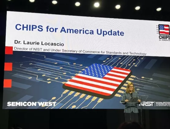
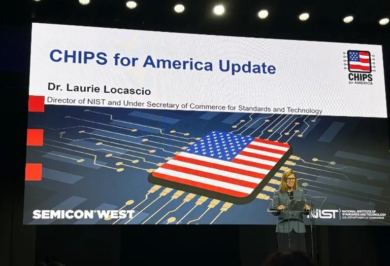
SEMI was honored to welcome U.S. Under Secretary of Commerce for Standards and Technology, Dr. Laurie E. Locascio, to the CEO Summit keynote stage at SEMICON West 2024 on Tuesday, July 9. Locascio, who also serves as the Director of the National Institute of Standards and Technology (NIST), delivered her morning CHIPS Act Update keynote address to a packed room of over 1,000 attendees at the Moscone Center in San Francisco.During her address, Locascio emphasized how far the U.S. chip industry has progressed since 2021. “Prior to 2022 and the passage of the CHIPS and Science Act, the U.S. produced 0% of the world's leading edge chips,” she said. “But now, after these proposed investments, we've changed the global landscape.”Industry Shifts from the CHIPS and Science ActDue to long delays and price increases resulting from supply chain vulnerabilities, Locascio shared that Congress began developing the CHIPS and Science Act with two key goals in mind. The first, she said, was to protect economic security, and the second, was to lower costs for American taxpayers. As part of the CHIPS and Science Act, CHIPS for America was established to advance semiconductor manufacturing in the U.S. CHIPS for America encompasses two offices: The CHIPS Research and Development Office, as well as the CHIPS Program Office - both of which are responsible for implementing CHIPS and Science Act law.CHIPS for America, said Locascio, couldn’t be another procurement program. Instead, it needed to be a purpose-driven approach to build domestic manufacturing capacity. Locascio highlighted that CHIPS for America galvanized several experts from the federal government, R D, and other core areas to work together to revitalize the U.S. semiconductor industry and increase capacity. To achieve this, Locascio pointed to CHIPS for America’s $30 billion in proposed direct funding and $25 billion in proposed direct loans.Locascio also noted diversity of technology as being essential for the American chip industry, citing how Intel, Micron, TSMC, and Samsung have recently expanded in the U.S., with SK Hynix planning to build a fab and R D facility in Indiana. No other economy in the world, she said, has more than two of these companies producing leading edge chips on its shores.“The total public and private investment from our four, leading-edge companies will equal roughly $300 billion between now and the end of the decade, far and away the most investment in new production in the history of the U.S. semiconductor industry,” said Locascio. Industry Investments on the HorizonTo further aid these efforts, Locascio mentioned CHIPS for America’s notice of intent to invest $1.6 billion in an open competition to accelerate advanced packaging domestically and encourage innovation. Funding will be directed toward five key R D areas, including equipment tools, power delivery, connector technology, chiplets, and Electronic Design Automation (EDA), she said. Additionally, Locascio shared that CHIPS for America recently announced its first preliminary memorandum of terms (PMT) to support the upstream supply chain, and shared plans to announce several more PMTs in the future. Lastly, Locascio revealed that CHIPS for America plans to release a model and process for bringing new facilities to life, in partnership with the National Semiconductor Technology Center (NSTC). NSTC members, she said, will gain access to partnership funds and state-of-the-art facilities to support the U.S. semiconductor industry. “Across all these efforts, from manufacturing incentives to research funding, to workforce development efforts, the U.S. must cultivate and build our competitive assets to protect and grow our technological leadership,” said Locascio.In a podcast with Francoise von Trapp of 3D InCites recorded at SEMICON West, Locascio discussed her career background, CHIPS Act investments and the path forward for the semiconductor industry in the U.S. To learn more, check out the podcast interview with 3D InCites. SEMI Global AdvocacyDiscover how SEMI Global Advocacy Public Policy supports the microelectronics industry across trade, taxes, talent, and R D.John Cooney is Vice President of Global Advocacy and Public Policy at SEMI.
Read More
Per- and polyfluoroalkyl substances (PFAS) are a large class of thousands of synthetic chemicals that are used throughout the semiconductor industry in the form of gases, liquids, and solid high-molecular weight polymers, due to their wide range of physical and chemical properties. PFAS contain carbon-fluorine bonds, which are one of the strongest chemical bonds in organic chemistry, allowing them to resist degradation and to cover long distances away from the source of their release.In recent years, the high persistence of PFAS in both the environment and the human body has encouraged the European Chemicals Agency (ECHA) to launch a PFAS restriction proposal aiming to regulate and eliminate their use over the next few years. The proposal is currently under assessment by ECHA’s scientific committees for Risk Assessment (RAC) and for Socio-Economic Analysis (SEAC).PFAS in the Semiconductor Industry The exceptional physiochemical properties of PFAS provide them a high degree of functionality in semiconductor manufacturing across the entire supply chain, and often the combination of their properties allows manufacturers to satisfy multiple and overlapping technical requirements.While the industry recognizes the importance of transitioning away from PFAS, and research to that effect is ongoing, current technological limitations do not allow the industry to manufacture semiconductors without the use of PFAS or to discover scientifically viable alternatives that can effectively substitute their use.At this point in time, no known alternatives exist for most of the uses of PFAS by the semiconductor industry. Alternative substances must be researched, invented and potentially applied into mass production to be recognized as viable alternatives. Many different pathways will have to be explored as PFAS are currently used across the entire supply chain for over 1,000 semiconductor applications, including articles, support equipment and fab operations, or as process chemicals.SEMI Europe—European Semiconductor Industry Association (ESIA) PFAS Research Workshop Considering the criticality of the PFAS issue for the semiconductor industry, SEMI and the European Semiconductor Industry Association (ESIA) have greatly strengthened their joint advocacy efforts over this past year concerning the ECHA’s PFAS restriction proposal.In this regard, SEMI and ESIA successfully organized a workshop in October 2023 with the relevant representatives of the European Commission (DG GROW, DG ENV, DG CNECT and DG RTD) to present and discuss in-depth the key technical evidence for the use of PFAS is the semiconductor sector. The discussions built upon the extensive technical evidence that was presented by SEMI and ESIA in their respective submissions for the six-month PFAS consultation facilitated by ECHA.Following the successful execution of this first workshop, there was a keen interest from the European Commission to enquire further upon the current state of play of research and development efforts in the field of PFAS detection, abatement, capture and destruction, circularity, recycling and alternativesFor this reason, after the first workshop, ESIA and SEMI collaborated to develop and deploy a joint PFAS Survey aimed at identifying the research priorities in PFAS from the perspective of their member companies. Based on the survey outcomes, the associations compiled the SEMI–ESIA PFAS Research Roadmap and officially presented it to the representatives of the European Commission during a follow-up workshop on 13th June 2024. Discussions at the workshop focused on the key research priorities for the semiconductor industry to discover potentially viable alternatives to the use of PFAS. In the upcoming legislative period, SEMI Europe will continue to engage with relevant stakeholders to contribute to the political debate and encourage a legislative framework that can enhance sustainability across industrial supply chains while preserving Europe’s technological competitive advantage. Get InvolvedGet involved in the SEMI PFAS Working Group! The SEMI PFAS Working Group is composed of industry technologists from leading companies across the global semiconductor manufacturing supply chain. The working group meets regularly to share intelligence and develop strategies to earn exemptions and/or extensions from regulators. Join SEMI in this crucial effort to enable the industry to continue manufacturing chips vital to the prosperity of the world by contacting [email protected]. Stefano Orlando is Manager Advocacy and Public Policy at SEMI Europe.
Read More
As the semiconductor industry works to attract talent to overcome its labor shortage, governments, educators, and the private sector must collaborate to make industry career opportunities more accessible for prospective employees. This concept provided the framework for a panel discussion during SEMI’s 35th annual Advanced Semiconductor Manufacturing Conference (ASMC) that took place in Albany, New York in mid-May.Despite extensive CHIPS and Science Act news coverage and escalating efforts to promote semiconductor career development initiatives, there’s still a tremendous amount of work to do, noted Fran Dillard, Vice President and Chief Diversity Inclusion Officer at Micron. “We're going to have to work to reduce barriers to this industry, and we have a chance to make a generational difference for American citizens,” she said. The panel, titled Talent Pipeline: Building a Sustainable and Diverse Semiconductor Workforce, featured Dillard and representatives from government and education who shared insights on growing the industry to fulfill unprecedented chip demand. Dillard was joined by Kylie Patterson, Chief Opportunity and Inclusion Officer at CHIPS for America; Kevin Younis, Chief Opportunity Officer and Executive Deputy Commissioner at Empire State Development; and Hector M. Rodriguez, Ph.D., Dean of Science, Technology, Engineering and Math at Hudson Valley Community College. Shari Liss, Executive Director of the SEMI Foundation, moderated the panel.Building the Future Together The need for extensive collaboration to bring semiconductor manufacturing back to the United States fueled the discussion. Patterson explained that given current investments in the semiconductor industry, the U.S. must double its workforce and triple its graduates in technical and construction-related fields. Overall, she estimated the industry will need to train around 100,000 new technicians.To achieve these goals, Rodriguez said that representatives from GlobalFoundries, the New York State Department of Labor, State University of New York, Center for Economic Growth, and the National Institute for Innovation and Technology, meet monthly to discuss on-the-job training programs for high school graduates and General Educational Development (GED) holders. He explained that by frequently evaluating training programs, they can quickly adjust curriculums if results don’t meet expectations. Younis said that bringing manufacturing back to the U.S. creates a unique alignment of interests between the government and the private sector. He highlighted the opportunity to work together to build the country’s manufacturing capacity, citing Empire State Development and Micron’s Green CHIPS Community Investment Fund for Central New York as an example of public and private collaboration. Part of the fund, he explained, will go toward workforce development. “We can focus on succeeding, with everyone marching in the same direction,” he said. Tapping Underrepresented Populations To find the talent needed to sustain the pace of semiconductor innovation, the panel stressed the importance of attracting people from all backgrounds and exposing them to the industry earlier in life. Dillard pointed out that women account for just 10-15% of workers in technical roles, and that percentage is even lower for people of color. “If we’re going to resource the semiconductor industry over the next 10-20 years, we’ve got to bring everyone with us,” she said.Helping those from underrepresented communities overcome barriers like limited access to childcare and transportation is important, said Rodriguez. He noted that wraparound services can be essential for transitioning these individuals into industry careers. Younis also highlighted Empire State Development’s One Network for Regional Advanced Manufacturing Partnerships (ON-RAMP) program, which will help provide these services in Upstate New York. If we’re going to get the people the industry needs, we must look for every opportunity, Rodriguez said, as they need to see that a great job is on the other side of the fence. Patterson said schoolchildren should be exposed to the semiconductor industry at a younger age, particularly girls and those from underrepresented groups. She cited a study about LEGO blocks, explaining that when the toy is introduced in primary school, boys are often excited, but girls are generally uncomfortable. “This is an example of the role of exposure,” she said. “If you’re not exposed to something, you have a lack of comfort, and that lack of comfort means you also have a lack of persistence to arrive at a level of competence.” Retaining the WorkforceAs an example of how to retain employees, Dillard pointed to the success of Micron’s Employee Resource Groups, as evidenced by the company’s internal data. These groups offer space for Micron’s underrepresented populations to connect with peers from similar backgrounds. Currently, the company has 10 groups, including groups for veterans, women, disabled employees, racial groups, and others. Diversity within leadership was also noted as key for retaining employees. Rodriguez said that when employees see people from similar backgrounds to their own in leadership roles, those employees are more likely to stay with those companies. Leadership training around psychological safety and working cross-culturally was also mentioned, with Dillard highlighting the importance of developing leaders that value inclusion. The cyclical nature of the industry was addressed during the Q A as a reason people may not stay long-term. Part of the solution, Patterson said, is to be transparent about market challenges and the importance of having a few months’ worth of savings. When employees encounter market challenges, they may be forced to switch industries if they don’t have savings to cover them. “There’s a role for us to be playing when it comes to supporting the financial literacy of our employees,” she said. View the full 2024 panel discussion to learn more. Additional ASMC 2024 HiglightsASMC 2024 featured keynotes by thought leaders from IBM, Wolfspeed, and Semiconductor Advisors. ASMC is the leading international technical conference for discussing solutions that improve the collective manufacturing expertise of the semiconductor industry. Solving the challenges presented by semiconductor manufacturing is a combined effort by device makers, equipment and materials suppliers, and academics. ASMC provides a platform for semiconductor professionals to network and learn the latest in the practical application of advanced manufacturing strategies and methodologies. Technical presentations at ASMC highlight industry innovations with specific results and select ASMC manuscripts are published in the ASMC Special Section of IEEE Transactions on Semiconductor Manufacturing.Krish Raghunath is Sr. Specialist for Conferences Committees at SEMI Americas.
Read More