
Now that’s dope!
Doping is a major problem in professional sports. But what about in chipmaking?
Electron doping is fundamental to semiconductor manufacturing. The process involves intentionally adding impurities to a pure (undoped) semiconductor, allowing engineers to modulate its electrical, optical, and structural properties. By adding a small percentage of atoms with five valence electrons, like arsenic to silicon, extra electrons are introduced, making the material more conductive.
Carefully controlling doping levels and types in semiconductors enables engineers to tailor the electrical properties to meet diverse technological needs, from high-speed chips to efficient solar cells for renewable energy applications.
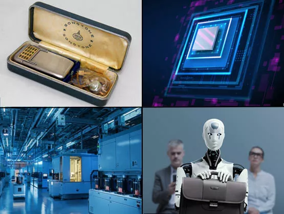
Can you hear me now?
Beginning in the 1920s, hearing aids used vacuum tubes to increase sound levels. The first commercial product in the U.S. to use a transistor was a $229.50 hearing aid from Sonotone in 1952, five years after the invention of transistors. The device combined two vacuum tubes and a transistor made by Germanium Products Corporation. By 1954, 97% of all hearing aids relied solely on transistors.
Tokyo Telecommunications Company, which later became SONY, also sold hearing aids and continues to do so today. These first hearing aids were clunky and not very discreet. Modern hearing aids are sleek, in some cases almost invisible, and have an amazing capacity to improve hearing rather than simply amplify sound.
More importantly, can it defend the galaxy?
Project GROOT, not to be confused with the Marvel Comic which debuted in 1960, stands for Generalist Robot 00 Technology. Nvidia’s robotic GROOT, which debuted earlier this year at Nvidia GTC 2024, will be used in robots to understand natural language and emulate movements by observing human actions to learn coordination, dexterity and skills to navigate and adapt to the real world.
By adding generative AI components to the company’s existing hardware and software platform for robots, Project GROOT will have sufficient power to help humanoids perform complex tasks and interact with real humans and machines.
Fabs sprouting up all over!
Spurred in large part by CHIPS and Science funding, about 24 semiconductor fabs are currently under construction across the U.S., including TSMC Arizona. The total value of these projects through 2030 is estimated to approach $250 billion. That’s $3 billion more than the Gross Domestic Product of New Zealand!
Do you have a fun fact to share? We invite SEMI members to share fun facts about the industry or their company. We’ll consider your tidbits for inclusion in future blog articles and or posting on social media. Complete our survey form or email [email protected].
Learn more about the SEMI Foundation and its initiatives to promote industry awareness and help provide a path for those interested in rewarding careers in microelectronics.
Follow the SEMI Foundation on LinkedIn, Instagram, Twitter and Facebook.
Margaret Kindling is Senior Program Manager for Diversity, Equity, and Inclusion at the SEMI Foundation. She promotes inclusion and diversity via Foundation activities such as Women in Semiconductors, PRIDE in Semiconductors and SEMICON West Workforce Development Pavilion programming.


