downloadGroupGroupnoun_press release_995423_000000 copyGroupnoun_Feed_96767_000000Group 19noun_pictures_1817522_000000Member company iconResource item iconStore item iconGroup 19Group 19noun_Photo_2085192_000000 Copynoun_presentation_2096081_000000Group 19Group Copy 7noun_webinar_692730_000000Path
Skip to main content
Default Banner Image

Technology and Trends

Emboldened by advances in self-driving and Internet of Vehicles (IoV) technologies, Taiwan’s microelectronics sector is investing heavily in manufacturing processes and equipment as engines of innovation and growth for autonomous driving, the world’s next market goldmine. But breaking into the self-driving vehicle industry can be a steep uphill climb. Semiconductor players hungry to secure their piece of the potentially massive market must know how to navigate the automotive industry’s unique ecosystem of suppliers, not to mention its lofty standards for safety and reliability.To explore opportunities and challenges in the automotive semiconductor market, SEMI recently organized Mobility Tech Talk – a gathering of experts from Strategy Analysis, Yole Développement, Renesas, X-FAB and IHS Markit who examined the evolution of sensors for autonomous cars, advanced driver-assisted system (ADAS) applications, and new energy vehicles (NEVs) in China. Nearly 200 participants exchanged in-depth, forward-looking insights and perspectives as the event helped forge stronger relations among various market segments. Here are four key takeaways from the conference. Lidar: The Hottest Sensing Technology for Smart AutomotiveLidar, mmWave radar, cameras and inertial measurement units (IMUs) are critical sensing devices for autonomous cars. With sensor and high-speed computing technologies maturing at their current pace, some 350,000 self-driving vehicles are expected to hit the road by 2027. But before a single autonomous vehicle takes to the roadways, self-driving technology must become expert at monitoring a vehicle’s environment.That’s where Lidar, the hottest of all sensing technologies and the key to the holy grail of safe self-driving, comes into the picture. Lidar’s versatility supports multiple essential functions such as mapping, object detection and object movement. The problem is that mass production is still impossible due to the technology's high costs. What’s more, technical issues must still be sorted out with solid-state lidar, mechanical lidar and MEMS. Both startups and traditional tier-1 semiconductor manufacturers are aggressively investing in related research and development in hopes of fulfilling lidar's promise and seizing the market opportunity. Smart Automotive Sets New Quality and Safety StandardsAs cars become smarter, so too must silicon. Chips must support vastly more data generated by in-vehicle connectivity, ADAS, electrification, autonomous driving and an array of other functions that rely on advanced automotive electronics components. With demand for smarter silicon surging, Taiwan semiconductor companies are turning to the automotive chip industry for expertise and serving as OEMs for major automakers.Quality and safety for automotive applications is paramount. In-vehicle semiconductors must meet strict requirements for vehicle control, robustness, liability, cost and quality management to meet the automotive specifications necessary to securing certifications. Smart silicon must also pass all AEC-Q liability standards promoted by North America automakers and score “zero defect” for the ISO/TS 16949 Automotive Quality Management System.China’s New Energy Vehicles To Fuel Semiconductor GrowthTo promote NEVs and reduce fuel consumption of cars with internal combustion engines (ICEs), late last year the Chinese government introduced the Measures for the Parallel Administration of the Average Fuel Consumption and New Energy Vehicle Credits of Passenger Vehicle Enterprises. With China the world’s largest market for NEVs, the policy is forcing automakers in Japan, the U.S. and Europe to accelerate moves towards NEVs that, in turn, will fuel growth in the semiconductor and automotive battery industries. NEVs in China are expected to number 2 million by 2020 before more than doubling to 4.9 million by 2025. Today, most cars still run on ICEs as environmentally friendly motor drives are still under development. In unit shipments, motor drives are expected to surpass ICEs by 2025.Cross-field Collaboration is KeyThe rise of smarter, fully autonomous vehicles – a disruptive Car 2.0 – is unlikely to happen overnight. Rapid growth of the global automotive semiconductor market will continue, with safety and powertrain applications driving the strongest chip demand. Meanwhile, automakers are focusing more on innovations from startups and non-traditional suppliers, and some have even started to develop their own IP and solutions. These paradigm industry shifts are diversifying the automotive supply chain into a cross-domain collaborative network of suppliers, pushing the closed, one-way automotive supply chain into lesser relevance. In the near future, rivals and partners may become indistinguishable as traditional turf wars begin to wane. As ADAS and autonomous cars evolve, and the era of electric cars nears, automotive semiconductors are emerging as the engine of growth for the global semiconductor industry. The automotive semiconductor market is expected to grow at a CAGR of 5.8 percent, reaching US$48.78 billion by 2022.For its part, the SEMI Smart Automotive special interest group connects professionals from the microelectronics and automotive industries. The group promotes the semiconductor industry's development of automotive technologies and cross-domain collaboration to help drive autonomous vehicle innovation.
Read More
SEMI’s Nano-Bio Manufacturing Consortium (NBMC) is in the news again for collaborating on the development of a patch that monitors hydration by measuring electrolyte levels in sweat. The innovative sweat patch is featured in this story by Defense Visual Information Distribution Service (DVIDS).“Born out of an AFRL (Air Force Research Laboratory) and industry collaboration within the Nano-Bio Manufacturing Consortium (NBMC), a wearable patch is helping researchers make ‘sense’ of the link between sweat and hydration,” the article notes.NBMC is a diverse group of companies, universities and organizations that brought their enthusiasm and interdisciplinary smarts across nanotechnology, biotechnology, advanced (additive) manufacturing, and flexible electronics to tackle the challenge of underhydration and dehydration for people with high-stress, high performance occupations. The idea was to develop a device that delivers reliable, wireless, actionable human performance data in a non-invasive way.The team is currently concentrating its efforts on a next-generation of sweat patches that will take what they developed, refine it and even incorporate other sweat-assessment capabilities.Certainly, the world is their oyster as the patch received recognition at this year’s 2018FLEX conference in February. The article notes:“The sweat patch development team received the 2018 FLEXI Award for R D Achievement at the SEMI FLEX Conference and Exhibition in Monterey, California. FLEXI awards recognize groundbreaking accomplishments in the Flexible Hybrid Electronics sector. The award-winning team is comprised of researchers from the Air Force Research Laboratory, GE Global Research, UES, Inc., the University of Arizona, University of Connecticut, University of Massachusetts Amherst and Dublin City University.”Kudos to the team! We couldn’t be more excited about future developments!Want more information? Be sure to check out our last blog post on GE's extensive report on the project. Also, visit www.nbmc.org for more information.NBMC is hosting a Smart MedTech TechXPOT on Digital Medicine and Remote Patient Monitoring at SEMICON West on July 12, 2018 from 10:30 AM to 12:30 PM. Listen to healthcare industry leaders explore state of the art and what is on the horizon for this medical technology space. Registration is now open.
Read More
With technology moving at breakneck speed, MEMS and sensors professionals whose job is to stay on top of industry developments must be able to find useful information—fast. Podcasts are one rich source of insight. In All Ears, I share roundups of recent podcast interviews with entrepreneurs and CEOs and episodes covering emerging technologies, breakthroughs and even the unexpected – like a MEMS pinball machine. For the seasoned MEMS and sensors professional or the curious onlooker who loves to learn, here are 5 podcast episode recommendations. 1. Embedded.fm – Episode 214: Tiny Sensor ProblemsChristopher White (@stoneymonster) and Elecia White (@logicalelegance) host Embedded.fm, a weekly podcast about the 5Ws of engineering. They’re both embedded software engineers by trade and their guests include everyone from entrepreneurs and makers to educators and engineers.Tiny Sensor Problems is a good introduction for people who have little to no knowledge of MEMS sensors. Kristen Dorsey, Assistant Professor of Engineering at Smith College, provides a brief overview of MEMS and touches on the manufacturing processes, including temperature sensitivity and sensors hype over the years. You’ll learn facts about interesting MEMS applications that were created, like the pinball machine I mentioned. Dorsey also elaborates on her work in flexible strain and pressure sensors for possible applications in AR and robotics in the future. 2. NPT – Episode 4: MEMS Directional SensorsLet’s dig deeper and learn about some of the applications for MEMS and Sensors. In this case, Erdos Miller, The Drilling Technology Podcast focuses on an extreme niche: oil and gas drilling technology. Ken Miller and David Erdos make up two of the engineering, developers and architect team at Erdos Miller that specializes in creating custom solutions for oil and gas downhole devices. Throughout the episode, they explore surveying sensors starting from the 1920s. History buffs would appreciate the stroll down memory lane and the ingenuity behind the first survey sensor, which involved a glass bottle filled with acid. Texas Instruments’ DLP technology gets a mention towards the end of the episode when micromirrors became a topic of discussion. 3. The Early Stage Podcast – Episode 15: Vesper – Tiny Microphones That Listen ForeverMEMS and sensors are a huge part of IoT—no doubt about it. The Early Stage Podcast captures insights from entrepreneurs into their company’s journey including their innovative approaches to developing cutting-edge technologies and overcome business and technology challenges they encounter. This episode focuses on Matt Crowley, CEO at Vesper, and how piezoelectric microphones will affect the voice interfaces as AI grows more sophisticated. Enthusiastic about the subject, John Valentine, host of the Early Stage Podcast, poses thoughtful questions and Crowley is eloquent and clearly passionate about his trade. They touch upon the race to produce the best voice interfaces for the AI ecosystem and tool kits for companies interested in voice enablement—but lacking a dedicated audio team—and looking for a simple solution. 4. IoT Podcast – Episode 155: New toys, Pi Day and insect-tracking LIDARHost Stacey Higginbotham, a technology journalist covering cloud computing, data centers and IoT, joins IT expert and veteran podcaster Kevin Tofel, in a weekly conversation about IoT developments. They’re entertaining and informative with a knack for making complex concepts easily digestible. In this episode, they discussed their thoughts on how the Broadcom/Qualcomm merger played out. While not explicitly focused on MEMS and sensors, the episode and the podcast in general touches upon overarching challenges the MEMS and sensors industry faces with security, standards, product development and applications usage. The highlight of the show included the guest of this week, Tobias Menne, global head of digital farming at Bayer AG who discusses Agriculture Technology (AgTech). 5. Amelia’s Weekly Fish Fry – Silicon Stagnation: How Emerging Technologies and Non-Traditional Materials Are Changing the Future of MEMSHosted by visionary Amelia Dalton, this episode of Fish Fry addresses the prospect of paper and plastic displacing silicon in MEMS manufacturing. Dalton interviews A.M. Fitzgerald Associates founder Alissa Fitzgerald about her research on the threat of waning research to silicon sensor technology. And more importantly, they discuss its implications for the MEMS and sensor industry 10 to 20 years down the line.Can’t get enough of MEMS? Register to listen in on MEMS and Sensors Industry Group’s free webinar, “Process Control and Root Cause Analysis for More-than Moore and Advanced IC Technologies” on April 25 at 8:00 AM PDT.
Read More
Automakers are currently evaluating prototypes of Viper from AdaSky, a Far Infrared (FIR) thermal camera that embeds custom silicon co-designed with and manufactured by ST in 28nm FD-SOI. The complete sensing solution aims to enable autonomous vehicles to see and understand the roads and their surroundings in any condition. “With the help of ST, we have created the first high-resolution thermal camera for autonomous vehicles with minimal size, weight, and power consumption--and no moving parts. ST’s access to, and expertise in, ultra-low-power design, IP that is fully qualified for automotive applications, and 28nm FD-SOI technology have been vital to meeting the severe power constraints that would challenge our sensors’ performance,” said Amotz Kats, Vice President Hardware, AdaSky. “We’re in a position to deliver a breakthrough solution to revolutionize and disrupt the autonomous vehicle market because of ST’s mastery of automotive qualification and its strong manufacturing supply chain, which grants reliability, long-term support, and business continuity to car makers throughout the whole life of their production.” Passive infrared vision, like that in AdaSky’s Viper, when used in a fusion solution, can help close the gaps to provide accurate sight and perception without fail in dynamic lighting conditions, in direct sunlight, in the face of oncoming headlights, and in harsh weather. The new camera uses an FIR micro-bolometer sensor to detect the temperature of an object. In an ADAS solution, Viper uses proprietary algorithms based on Convolutional Neural Networks to classify obstacles and show them in a cockpit display to give the driver an early warning. This warning comes several seconds earlier than it would when using a conventional sensor in the visible wavelength and is even faster than what is possible with the human eye. The two companies say that the Far-Infrared thermal camera extends ADAS sensor fusion capability with a new layer of information, helping pave the way to fully-autonomous driving in any condition. Prototypes are now under evaluation by carmakers with initial production targeted for 2020. (Read the full press release here.)
Read More
GlobalFoundries' new ecosystem partner program, called RFwave™, aims to simplify RF design and help customers reduce time-to-market for a new era of wireless devices and networks (read the full press release here). The program aims to give designers a low-risk, cost-effective path to highly optimized solutions that leverage GF's platforms including RF on FD-SOI and RF-SOI. The target is wireless applications such as IoT across various wireless connectivity and cellular standards, standalone or transceiver integrated 5G front end modules, mmWave backhaul, automotive radar, small cell and fixed wireless and satellite broadband. As such, the RFwave™ partner program provides GF customers with IP design elements, EDA tools, design consultation and services and OSAT product packaging and test solutions. These products and services are validated, and comprise a plug-and-play catalog of design solutions. With this level of integration, GF customers can create high-performance designs while minimizing development costs. Bami Bastani, senior vice president of GF’S RF Business Unit, says, “As a leader in RF, GF’s RFwave program takes industry collaboration to a new level, enabling our customers to build differentiated, highly integrated RF-tailored solutions that are designed to accelerate the next wave of technology.” Initial members of the RFwave Partner Program are: asicNorth, Cadence, CoreHW, CWS, Keysight Technologies, Spectral Design, and WEASIC.
Read More
Worried that you’re underhydrated after a heart-pounding run or bike ride? SEMI’s Nano-Bio Manufacturing Consortium (NBMC) has you covered – with a patch. A few years after the group undertook the sweaty task of creating a non-invasive health monitor, the patch that tracks electrolyte levels recently ended up stuck to the skin of U.S. Air Force volunteers.“During extra workout sessions at the Air Force Research Laboratory in Ohio, the volunteers wore on their backs adhesive patches that collected their perspiration," according to GE Reports. "Sensors in the patches were able to detect the specific levels of electrolytes in the sweat the volunteers released. That data was transmitted wirelessly to a laptop computer app where researchers could analyze it in real time.” Read more about the project in the GE Reports blog.The project came together when NBMC, a diverse group of companies, universities and organizations, brought their enthusiasm and interdisciplinary know-how across nanotechnology, biotechnology, advanced (additive) manufacturing, and flexible electronics to tackle the challenge of underhydration and dehydration. The idea was to develop a device that delivers reliable, wireless, actionable human performance data in a non-invasive way.Congratulations to GE Global Research, and the partners from the Air Force Research Laboratory, University of Connecticut, University of Massachusetts-Amherst, American Semiconductor Inc., University of Arizona, UES, Dublin City University and NBMC on these impressive strides in the field of health monitoring!Watch this video to see the patch in action! (https://www.facebook.com/GE/videos/1667584156643205/)Visit www.nbmc.org for more information.
Read More
Sales revenues for fluid management subsystems grew 28 percent in 2017 to $1.28 billion, breaking the $1 billion mark for the first time. Fluid management subsystems have now seen five years of consecutive growth, and 2018 is expected to extend the growth streak to six years for the segment.Fluid management subsystems control the delivery of process gases and chemicals onto the wafer during processing and may be located either on-tool or near the tool. This segment can be further divided into two main categories – gas delivery and liquid delivery subsystems. Gas delivery subsystems, such as mass flow controllers (MFCs), deliver gases or speciality chemicals to a vacuum process chamber, and liquid delivery subsystems typically deliver liquid chemicals to a wet processing module. Demand for gas and liquid delivery subsystems is roughly 54 percent and 46 percent respectively – a ratio that has not changed significantly over the past few years.Although fluid management subsystems account for approximately 10 percent of expenditures on all critical subsystems used on semiconductor manufacturing equipment, growth of other critical subsystems such as vacuum processing subsystems has been sluggish.Mass flow controllers (MFCs), however, are showing strong growth potential and are set to buck their historical slow growth trend as the industry transitions into sub 10 nm processing. At the leading edge, processes are becoming more vacuum intensive and the importance (and difficulty) of accurately controlling chemical delivery for deposition onto the wafer is increasing. Process operating windows are getting tighter and the specification ranges demanded by chipmakers are shrinking, posing challenges for existing MFC technology. The upshot is that new MFC solutions and technologies are needed to enable transitions to smaller nodes, providing an opportunity for growth in this segment.The fluid management subsystems market is currently dominated by Japanese- and U.S.-based vendors. Horiba is the largest player, accounting for 30 percent of total fluid management sales, and the rest of the market is extremely fragmented, with a raft of companies competing in this space.Given the large size and fragmentation of this segment, interest in these products in the coming year is sure to intensify as the race to find lucrative solutions to enable sub 10 nm processing heats up.For more information about VLSI Research and Critical Subsystems, visit www.vlsiresearch.com.
Read More
Following the immense success of last year's FD-SOI training day in Silicon Valley, the SOI Consortium has another one planned for the end of April this year. If you want to start learning how to leverage FD-SOI in your chip designs, this is a great place to start. Click here for information on how to sign up. ST Fellow Dr. Andreia Cathelin has put together another great line-up. World renowned professors and experts from industry will deliver a series of four training sections of 1.5 hours each, focused on energy efficient and low-power, low-voltage design techniques for analog, RF, high-speed, mmW and mixed-signal design. You'll learn about design techniques that take full advantage of the unique features of FD-SOI, including body biasing capabilities that further enhance the excellent analog/RF performances of these devices. Each section of this training day will take you through concrete design examples that illustrate new implementation techniques enabled by FD-SOI technologies at the 28nm and 22nm nodes – and beyond. The design examples will cover basic building blocks through SoC implementations. A global Q A session will close the day. 
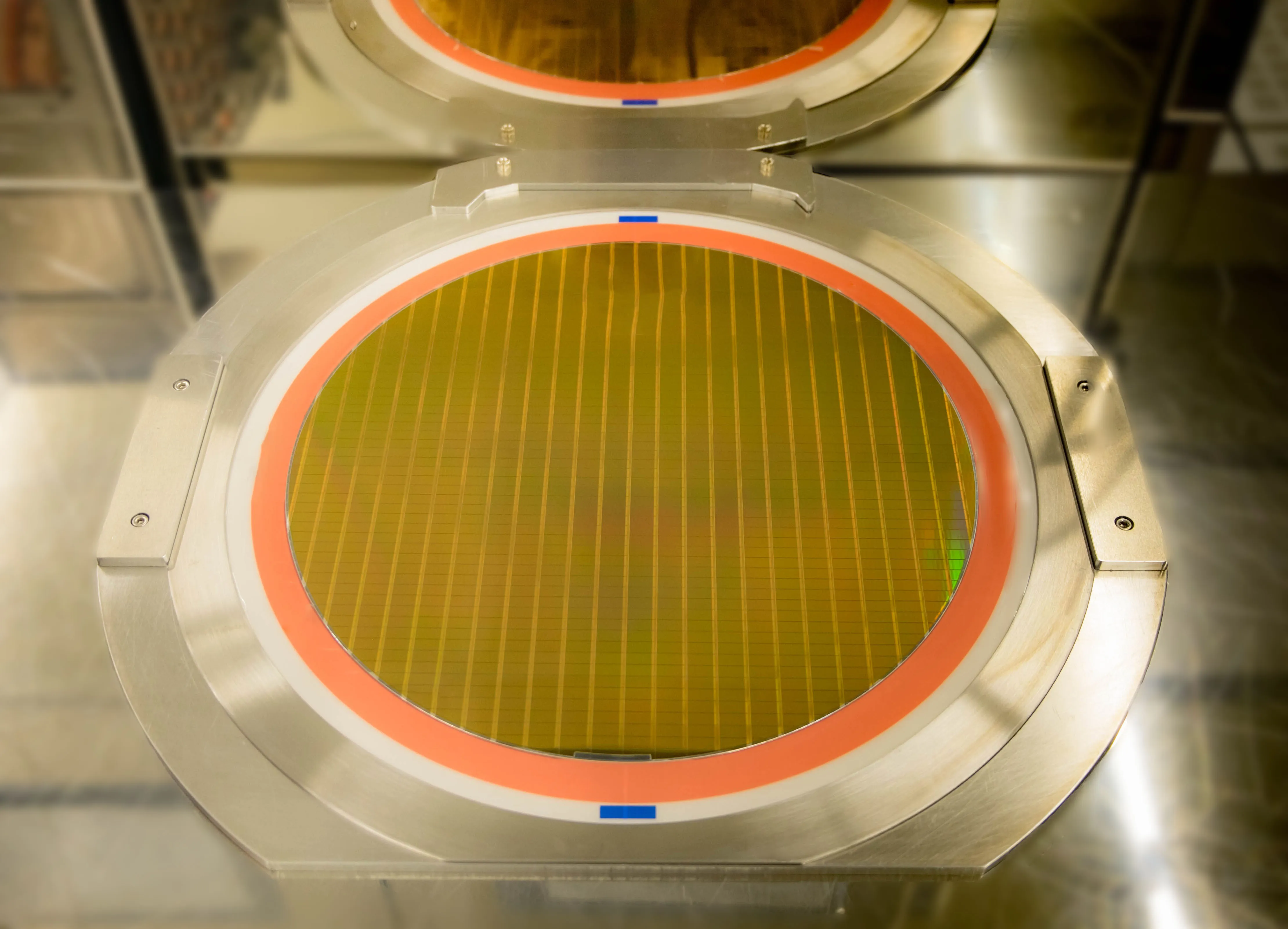
Here's a little more info on how the day will unfold. Click on the slides to see them in full screen. Morning sessionsFDSOI-specific design techniques for analog, RF and mmW applications - Andreia Cathelin, Fellow, STMicroelectronics [caption id="attachment_11714" align="alignleft" width="300"] Quick preview from Andreia Cathelin's FD-SOI training session (Courtesy: STMicroelectronics, SOI Consortium)[/caption] Andreia Cathelin is ST's key design scientist for all advanced CMOS technologies, and is arguably the world's leading expert on leveraging FD-SOI in high-performance, low-power RF/AMS SoCs. Her course will first present a very short overview of the major analog and RF technology features of 28nm FDSOI technology. Then the focus moves to the benefits of FD-SOI technology for analog/RF and millimeter-wave circuits. She'll give design examples such as analog low-pass filters, inverter-based analog amplifiers and 30GHz and 60GHz Power Amplifiers, as well as mmW oscillators. There will be particular focus on the advantages of body biasing and special design techniques offering state-of-the-art performance. Circuit Design Techniques in 22nm FD-SOI for 5G 28GHz Applications - Frank Zhang, Principal Member of Technical Staff, GlobalFoundries [caption id="attachment_11716" align="alignright" width="300"] Quick preview from Frank Zhang's FD-SOI training session (Courtesy: GlobalFoundries, SOI Consortium)[/caption] Frank Zhang has designed chips using GF's 22nm FD-SOI (22FDX) process for WLAN, 5G cellular and automotive radar applications. His course will focus on how to take advantages of FD-SOI’s high-frequency performance at relatively low-current density to design high performance RF/mmWave circuits. Examples circuits include a 28GHz LNA, a 28GHz PA and an RF switch for 5G applications. The FD-SOI advantages such as low capacitance, high breakdown voltage and high-output impedance will be exploited in these design examples. This course will also discuss how to extend these techniques to applications at higher frequencies and/or higher current densities that are subject to extreme temperatures and EM requirements. Afternoon sessionsEnergy-Efficient Design in FDSOI - Bora Nikolic, Professor, UC Berkeley [caption id="attachment_11715" align="alignleft" width="300"] Quick preview from Bora Nikolić's FD-SOI training session (Courtesy: UC Berkeley, SOI Consortium)[/caption] Borivoje (“Bora”) Nikolić is known as one of the world’s top experts in body-biasing for digital logic (he and his team have designed more than ten chips in ST’s 28nm FD-SOI.) If you missed it, his team's RISC-V chip was cited as one of Dr. Cathelin's “Outstanding 28nm FD-SOI Chips Taped Out Through CMP” – read more about that here. His talk at the training day will present options for energy-efficient mixed-signal and digital design in FD-SOI technologies. He'll explain how to generate body bias and use it to improve efficiency, with examples in RF and baseband building blocks, temperature sensors, data converters and voltage regulators. The techniques will be presented in the context of UC Berkeley's latest RISC-V-based SoC, designed to operate in a very wide voltage range using 28nm FD-SOI. mm-Wave and Fiber-Optics Design in FD-SOI CMOS Technologies - Sorin Voinigescu, Professor, University of Toronto [caption id="attachment_11713" align="alignright" width="300"] Quick preview from Sorin Voinigescu's FD-SOI training session (Courtesy: U. Toronto, SOI Consortium)[/caption] Sorin Voinigescu is a world renowned expert on millimeter-wave and 100+Gb/s ICs and atomic-scale semiconductor device technologies. His lecture will cover the main features of FD-SOI CMOS technology and how to efficiently use its unique features and suitable circuit topologies for mm-wave and broadband SoCs. He'll begin with an overview of the impact of the back-gate bias and temperature on the measured I-V, transconductance, fT, and fMAX characteristics. Then he'll compare the maximum available gain, MAG, of FDSOI MOSFETs with those of planar bulk CMOS and SiGe BiCMOS transistors through measurements up to 325 GHz. Next, he'll provide biasing, sizing and step-by-step design examples for VCO, doubler, switches, PA, large swing optical modulator drivers and quasi-CML circuit topologies and layouts that make efficient use of the back-gate bias to overcome the limitations associated with the low breakdown voltage of 20nm and 12nm FD-SOI CMOS technologies. Sign Up Now!With over 100 attendees filling every chair in the auditorium, last year's training day was sold out. Although it was in Silicon Valley, people actually flew in from all over the world to be there. During the Q A at the end, most everyone prefaced their questions by saying, “Thank you. I really learned a lot today.” 2018 will be no different – except that it's sure to sell out even faster. Please note, though, that this is not a free event, so only the attendees will get copies of the slide decks. Here's key info you need to sign up. See you there!What: SOI Consortium's FD-SOI Training DayWhen: 27 April 2018, 7:30am – 5pm.Where: Crowne Plaza San Jose, Milpitas CA (parking is free)Registration fee: US $485.00 (includes training book, breakfast, box lunch and refreshments during breaks)How to sign up: Click here to go directly to the registration site.
Read More
Artificial intelligence (AI) is making headlines everywhere, offering a range of capabilities, including location and motion awareness — determining whether a user is sitting, walking, running or sleeping. Behind the scenes, AI is capturing volumes of data. Makers of smartphones and fitness and sports trackers, along with application developers, are all clamoring for this data because it helps them analyze real-world user behavior in depth. Manufacturers gain a competitive edge by tapping this intelligence: Using it to improve user engagement, they increase the perceived value of their devices, potentially reducing customer churn. How can consumer-product manufacturers tap the built-in capabilities of MEMS inertial sensors — which are already ubiquitous in end-user devices — to make the most of AI? Machine learningProduct manufacturers can easily build an activity classification engine using commonly available smart sensors and open-source software. Activity trackers, for example, use raw data first collected via the MEMS inertial sensors that are already installed in smartphones, wearables and other consumer products.With the building blocks in place, consumer-product manufacturers can apply machine learning techniques to classify and analyze this data. There are several possible approaches, ranging from logistic regression to deep learning neural networks.One well-documented method used for classifying sequences in AI is Support Vector Machines (SVM). Physical activities, whether walking or playing sports, consist of specific sequential repetitive movements that MEMS sensors gather as data. MEMS sensors make good use of this collected data, which can be easily processed into well-structured models that are classifiable with SVMs.Consumer-product manufacturers have gravitated toward the SVM model since it is easy to use, scale and predict. Using an SVM to set up multiple simultaneous experiments for optimizing classification over diverse, complex real-life datasets is far simpler than with other approaches. An SVM also introduces a wide range of size and performance optimization opportunities for the underlying classifier.Cost impacts of processing, storage and transmissionIn practice, recognizing user activity hinges on accurate live classification of AI data. Therefore, the key to optimizing product cost is to balance transmission, storage and processing costs without compromising classification accuracy.This is not as simple as it sounds. Storing and processing AI data in the cloud would leave users with a substantial data bill. A WiFi, Bluetooth or 4G module would drive up device costs and require uninterrupted internet access, which is not always possible.Relegating all AI processing to the main processor would consume significant CPU resources, reducing available processing power. Likewise, storing all AI data on the device would push up storage costs.Resolving the issuesTo resolve these technology conflicts, we need to do four things to marry the capabilities of AI with MEMS sensors.First, decouple feature processing from the execution of the classification engine to a more powerful external processor. This minimizes the size of the feature processor size while eliminating the need for continuous live data transmission.Next, reduce storage and processing demands by deploying only the features required for accurate activity recognition. In one example created by UC Irvine Machine Learning Repository (UCI), when an AI model was trained using a dataset of activities with 561 features, it identified user activity with an accuracy of 91.84 percent. However, using just the 19 most determinative features, the model still achieved an impressive accuracy of 85.38 percent. Notably, pre-processing alone could not identify these determinative features. Only sensor fusion enabled the data reliability required for accurate classification. Third, install low-power MEMS sensors that can incorporate data from multiple sensors (sensor fusion) and enable pre-processing for always-on execution. A low-power or application-specific MEMS sensor hub can slash the number of CPU cycles that the classification engine needs. The onboard software can then directly generate fused sensor outputs at various sensor data rates to support efficient feature processing.Finally, retrain the model with system-supported data that can accurately identify the user’s activities.Additionally, cutting the data capture rate can reduce the computational and transmission resource requirements to a bare minimum. Typically, a 50 Hz sample rate is adequate for everyday human activities. This may soar, however, to 200 Hz for fast-moving sports. Reducing dynamic data rate selection and processing in this way lowers manufacturing costs while making the product lighter and/or more powerful for the consumer.High efficiency in processing AI data is key to fulfilling its potential, driving down costs and delivering the most value to consumers. MEMS sensors, in combination with sensor fusion and software partitioning, are critical to driving this efficiency. Operating at very low power, MEMS sensors simplify application development while accurately analyzing motion sensor data.Combining AI and MEMS sensors into a symbiotic system promises a new world of undreamt-of opportunities for designers and end users.This blog post is based on an original article that first ran in EDN. It appears here with the permission of the publisher.
Read More
Large semiconductor fabs can devour electricity at clip of 100 megawatts per hour -- enough to power 50,000 homes1 and, according to a McKinsey study, more than automobile plants and oil refineries consume. So ravenous is their electricity consumption that some fabs have resorted to building their own captive power plants. Oversize fabs, depending on their location and local rates, can run up utility bills as high as $25 million each year, with electricity accounting for up to 30 percent of operating costs.Fabs use electricity to power HVAC, run cooling water, and for basic infrastructure. But the vast majority of electricity is gobbled up by semiconductor manufacturing process tools and their sub-fab support equipment such as vacuum pumps and abatement systems. In a typical fab, as much as 44 percent of the electricity is consumed by the processing equipment2. It’s not so hard to imagine. Etch and deposition tools need power to strike and sustain plasma, with multiple 1,000+ Watt RF power supply feeds per chamber and four, six or more chambers per tool, and vacuum pumps spinning and abatement running. The power load adds up quickly. Watts and WattsThe good news is that process tools aren’t processing wafers all the time. The bad news is that, in the past, there was no good way for the fab to know when process tools and support equipment weren’t running processes. Turning equipment off, or reducing power when not processing, wasn’t coordinated and standby states weren’t defined for readiness for a seamless power-up and return to processing. So what to do? Take action. That just what industry volunteers did when they met within SEMI’s Standards program and defined an equipment “idle mode” (SEMI E167 and SEMI S233). More recently, a SEMI Standard (SEMI E1754) was developed to define energy saving modes – how process tools communicate with sub-fab equipment, to reduce utility consumption when wafers are not being processed by the tool. Importantly, it also provides guidance on the standby state to return to full performance when the tool is needed to process wafers.5Good to be IdleThe semiconductor industry is now increasingly adopting a “smart idle” approach using these SEMI Standards. Fabs implementing these standards to take advantage of process tool idle periods can save more than 4.3 million € annually, according to AIS Automation modeling.6 This study also points to a savings of more than 16,000 tons of CO2 per year, the equivalent of taking more than 10,000 cars off the road.Who knew that recognizing when to be idle could bring such big rewards? If only I could apply that to my own life, but, for now, I will have to leave it to the fabs. SEMI International Standards volunteers make a huge difference to our industry every day. If you want to join the over 5,000 SEMI Standards volunteers (or join SEMI’s Sustainable Manufacturing eForum), with representation from over 2,000 companies, it’s free! Don’t be idle for this one, click here to join! http://www.semi.org/en/standards/P041367 1Bringing Energy Efficiency to the Fab, McKinsey 20132http://semiengineering.com/saving-energy-in-the-fab/3SEMI E167-1213 - Specification for Equipment Energy Saving Mode Communications (EESM)http://ams.semi.org/ebusiness/standards/SEMIStandardDetail.aspx?ProductID=211 DownloadID=32573SEMI S23-0813 - Guide for Conservation of Energy, Utilities and Materials Used by Semiconductor Manufacturing Equipmenthttp://ams.semi.org/ebusiness/standards/SEMIStandardDetail.aspx?ProductID=211 DownloadID=31094SEMI E175-1116 - Specification for Subsystem Energy Saving Mode Communication (SESMC)http://ams.semi.org/ebusiness/standards/SEMIStandardDetail.aspx?ProductID=211 DownloadID=38765http://electroiq.com/blog/2017/06/how-semi-standard-e175-is-saving-energ...6SEMI Standards a Potential Help for Saving Energy, Bert Mueller, AIS Automation 2016
Read More