downloadGroupGroupnoun_press release_995423_000000 copyGroupnoun_Feed_96767_000000Group 19noun_pictures_1817522_000000Member company iconResource item iconStore item iconGroup 19Group 19noun_Photo_2085192_000000 Copynoun_presentation_2096081_000000Group 19Group Copy 7noun_webinar_692730_000000Path
Skip to main content
Default Banner Image

Technology and Trends

The MCU at the heart of Sony's new smart-sensing SPRESENSE™ for IoT is built on FD-SOI. Why? Low operating voltage and low power consumption, of course! Sony's got two cool new products going on sale in July 2018: the SPRESENCE main and extension boards for IoT applications, equipped with a smart-sensing processor (read the full press release here). A CXD5602PWBCAM1 camera board for sensing cameras will go on sale in August. All were on display at the SF Maker Fair '18, where they were an instant hit. [caption id="attachment_11931" align="alignright" width="300"] Here are the main features of Sony's CXD5602 MCU for IoT, which is built on FD-SOI. (Courtesy: Sony Semiconductor Solutions)[/caption] The main board (it's open source, btw) will run about US$50. You'll find the specs and main features here. Spresense is powered by Sony's FDSOI-based CXD5602 MCU (ARM Cortex-M4F × 6 cores), with a clock speed up to 156 MHz. The main board utilizes a multi-CPU structure equipped with Sony's state-of-the-art GNSS (Global Navigation Satellite System – which they talked about at the most recent SOI Symposiums in SF and Tokyo) receiver. A variety of systems for diverse applications, including drones, smart speakers, sensing cameras and other IoT devices, can be built by combining these boards and developing the relevant applications. The new board can be used to control a drone, for example, using GPS positioning technology and a high-performance processor, voice-controlled smart speakers, low-power consumption sensing cameras and other IoT devices, etc. It can also be combined with various sensors for use in systems that detect errors in production lines on the factory floor.
Read More
[caption id="attachment_11914" align="alignright" width="150"] Mark Granger, GlobalFoundries' VP Automotive Product Line Management[/caption] GF's 22FDX® (22nm FD-SOI) offering is on an automotive roll. The technology platform has been certified for several key automotive standards, and GF has announced an exciting new ADAS customer in Arbe Robotics. In addition to sharing info from various press releases and blogs, ASN also had a chance to catch up with Mark Granger, GF's VP for automotive, who provided some great insights. Read on! Taking the Heat When it comes to compliance, automotive industry standards are excruciatingly rigorous. Every part that goes into a car must adhere to the relevant standards: chips are no exception. One such standard is the AEC – Q100, a “Failure Mechanism Based Stress Test Qualification For Integrated Circuits”. The AEC – aka the Automotive Electronics Council – handles those testing standards and certification. Grade 2 means a technology is certified for the -40°C to +105°C ambient operating temperature range. To achieve Grade 2 certification, devices have to successfully withstand reliability stress tests for an extended period of time over the specified temperature range. GF recently announced that 22FDX has been AEC Q100 Grade 2 certified (press release here). However Granger adds that for their customers, they've added additional headroom that takes them to 125°C. They're now working on Grade 1 certification, he says, which means the devices are certified to handle junction temperatures up to 125°C (and there again, GF has added additional headroom that takes them to 150°C). That should be done by the end of 2018. The ability you get with FD-SOI to tune the transistors using body biasing is really beneficial here, he says. For GF, the 22FDX qualifications exemplifies their commitment to providing high-performance, high-quality technology solutions for the automotive industry. The automotive industry is driven by a “zero excursions – zero defects” mindset, says Granger, and that drives the foundry, too. SOI has been used for decades across industries where heat and electromagnetic radiation are challenges, bringing soft error rates (SER) down by orders of magnitude, notes Granger. (SOI, btw, essentially eliminates what are known as Single Event Upsets (SEU) caused by latch-up, which in turn brings down SER.) That in turn, ties into the FIT (failure in time) rate – and that's part of the ISO 26262 “Road vehicles – Functional safety” standard – where 22FDX is also certified. As a part of GF's AutoPro™ platform, 22FDX allows customers to easily migrate their automotive microcontrollers and ASSPs to a more advanced technology, while leveraging the significant area, performance and energy efficiency benefits over competing technologies. Moreover, the optimized platform offers high performance RF and mmWave capabilities for automotive radar applications and supports implementation of logic, Flash, non-volatile memory (NVM) in MCUs and high voltage devices to meet the unique requirements of in-vehicle ICs. GF's Fab 1 in Dresden, Germany (which is where they do 22FDX) also has achieved ISO-9001/IATF-16949 certification, which demonstrates that it is capable of meeting the stringent and evolving needs of the automotive industry. (IATF is the International Automotive Task Force. 16949 is a Quality Management System (QMS) certification specifically for the automotive sector.) Granger wrote a really informative blog on the GF website – you can read it here. It includes this graphic, indicating where in the car 22FDX-based parts are expected to go. [caption id="attachment_11913" align="alignleft" width="1000"] Here's how GF sees the applications for 22FDX and other chip technologies in automotive applications. (Courtesy: GlobalFoundries)[/caption] On Radar GF recently announced that Arbe Robotics selected 22FDX® as the process technology for its groundbreaking patented imaging radar. Arbe aims to achieve fully automated system capabilities and enable safer driving experiences for autonomous vehicles (read the press release here). As the first company to demonstrate ultra-high-resolution at a wide field of view, Arbe Robotics’ radar technology can detect pedestrians and obstacles at a range of 300 meters, in any weather and lighting conditions. The processor creates a full 3D shape of the objects and their velocity, and classifies targets using their radar signature. As Granger noted in his blog, “Radar is one of several sensor types used to detect objects near a vehicle, to enable features like adaptive cruise control. Lidar is another. It uses pulsed lasers to determine distance from an object by measuring the time it takes for the light to reflect back. However, lidar is currently expensive and is affected by weather conditions. Radar is less expensive, and higher-resolution radars promise to compete well with lidar in automotive applications, thereby enabling lower-priced vehicles to enjoy greater ADAS capabilities. 22FDX-based radar sensors can provide higher resolutions and less latency than current radar sensors at a very low total system cost.” While they may be complementary at first, there is a battle brewing between high-resolution radar and lidar, Granger told ASN. Putting their solution on 22FDX enables Arbe to achieve a 77 GHz mmWave radar and compete cost-effectively with lidar. “They wanted the best,” says Granger. 22FDX can achieve the requisite Ft and Fmax figures of merit. And with transistor stacking, they can also integrate the power amplifier (PA) on a single device. With the low inherent capacitance of the PA in 22FDX, you can get the high power output you need for mmWave but with low power consumption. GF blogger Dave Lammers has also written a great piece about the Arbe solution (you should read it: here's the link). “The company said its advanced technology allows the detection of small targets, such as a human or a bike even if they are somewhat masked by a large object such as a truck,” he writes. “The imaging radar can determine whether objects are moving, and in what direction, and alert the car in real-time about a risk. “While other car sensors can fail when it is raining, if there’s fog, and due to blinding lights such as a sudden reflection, Arbe’s radar is completely oblivious to all those factors. The custom designed radar processor creates a full real-time 4D image of the environment, and classifies targets using their radar signature.” Avi Bauer, Arbe's VP of R D, is now clearly an SOI fan. Lammers quotes him as saying, “With SOI the design is more straightforward, and (voltage) biasing allows you to do things that cannot be done in standard CMOS. For the transmit and receive modules, SOI’s higher resistivity substrate benefits the passive components – inductors and capacitors – and allows good isolation. High Q passives are important. At 22nm, SOI allows better performance overall.” Clearly good things are coming down the road for FD-SOI!
Read More
Self-driving cars have been all the rage in both the trade and popular press in recent years. I prefer the term “autonomous vehicles,” which more broadly captures the possibilities, encompassing not only small passenger vehicles but mass transit and industrial vehicles as well. Depending on who’s talking, we will all be riding in fully autonomous vehicles in five to 25 years.The five-year estimates come from startups eager to raise venture capital while the 25-year estimates stem from Tier 1 automotive suppliers who tend to be more conservative in outlook. Regardless of the timeframe, a multitude of investors – national governments, venture capitalists and companies – are dedicating significant capital and effort to make autonomous vehicles a reality.I must admit that I did not fully grasp the enthusiasm for self-driving cars until last year. First, I’ve always enjoyed driving, unless I’m in stop-and-go traffic, so I couldn’t imagine relinquishing the task. Second, I’ve deliberately arranged my life to spend minimal time in my car. However, traffic has become much heavier in my metropolitan area (Boston), and I know that many people in cities around the world face longer commutes and waste more time in gridlock.What is the solution to this problem that is only getting worse? I had an epiphany while walking through Shinigawa Station in Tokyo, one of the busiest train stations in the world. Dense streams of people crisscrossed the station on their individual paths, managing to avoid collisions without the aid of traffic controls. Evidently, humans have an innate collision-avoidance ability that makes traffic controls for pedestrian crowds unnecessary. If autonomous vehicles could achieve the same excellence in collision-avoidance, we could potentially reduce or eliminate traffic controls for vehicular traffic, providing a huge gain in transportation efficiency and relief from gridlock.Sensors as core building blocksNew and improved sensors, many based on micro-electromechanical systems (MEMS) technology, are key to achieving this vision. While MEMS inertial sensors (such as accelerometers and gyros) are already integral to the core safety systems in conventional vehicles, they are also essential to improved self-navigation in autonomous vehicles.The challenge for MEMS suppliers is to deliver inertial sensors that meet the requirements for self-navigation systems, which are different and more demanding than for safety systems.Pinpointing a vehicle’s position requires “dead reckoning” based on inertial sensor signals as a supplement to GPS input. Undesirable drift in the inertial sensor signals due to mechanical quadrature, temperature sensitivity and noise can quickly add up to a large error in position that may result in a collision. To meet the more rigorous requirements for autonomous vehicles, suppliers must design MEMS inertial sensors that are substantially more precise and resistant to drift. This requires design software that is both extremely accurate and fast, as well as increasingly precise and reliable manufacturing capabilities.Other MEMS-based devices, such as micromirrors and micro ultrasound transducers (MUTs), are also promising options for implementing vision and range-finding systems in autonomous vehicles. These sensing systems are needed for building electronic versions of the human collision-avoidance abilities that I witnessed in Shinigawa Station – and it is these systems that autonomous vehicles must emulate.When will self-driving cars become a reality? Aside from the provocative question that got you to read this far, I don’t have a definitive answer. It will undoubtedly occur in phases, ranging from the driver-augmentation systems available in today’s cars to the full autonomy and ubiquity that will allow reduction of traffic controls in 20 years or more. It is clear that the ultimate goals for autonomous vehicles are highly worthwhile, and that achieving those goals will require better-performing and more diverse MEMS sensors. Stephen (Steve) Breit, Ph.D. is Senior Director, MEMS Business, at Coventor, a Lam Research Company. Steve has been responsible for overseeing development and delivery of Coventor’s industry-leading software tools for MEMS design automation since joining Coventor in 2000. Steve holds numerous patents on software systems and methods for MEMS design automation and virtual fabrication. He holds a Ph.D. in Ocean Engineering from MIT and a B.S. in Naval Architecture and Marine Engineering from Webb Institute.For more information, visit: https://www.coventor.com
Read More
“GlobalFoundries, TowerJazz, TSMC and UMC are expanding or bringing up RF SOI processes in 300mm fabs in an apparent race to garner the first wave of RF business for 5G, the next-generation wireless standard,” writes Mark Lapedus of Semiconductor Engineering. His recent piece, RF-SOI Wars Begin, explains why demand across the supply chain is currently tight. Rest assured, the supply situation is being addressed fast. By next year, 300mm-based RF-SOI manufacturing (vs. 200mm) will increase from 5% to 20%. But with insatiable end-user demand for greater throughput, overall RF-SOI device demand is increasing in the double-digit range, so 200mm-based manufacturing is also expanding fast. [caption id="attachment_11905" align="alignleft" width="300"] The front-end modules in all smartphones are built on Soitec's RF-SOI wafer technology. The most advanced, for LTE/LTE-A, are built on Soitec's RFeSI-SOI wafers, which have four layers to meet the demands of devices with high linearity requirements. (Courtesy: Soitec)[/caption] SOI wafer manufacturer Soitec has 70% of the RF-SOI wafer market share. The other RF-SOI wafer manufacturers – Shin-Etsu, GlobalWafers and Simgui – all use Soitec's RF-SOI wafer manufacturing technology. This is an excellent, comprehensive piece, that clearly explains the complexities of the markets, the devices, the manufacturing and the supply chain. It's a highly recommended read. BTW, the SOI Consortium is organizing a 4G/5G SOI supply chain workshop during Semicon West (July '18). Sign up or get more information on that under the Events tab here on the consortium website. Of course, here at ASN, we've been covering RF-SOI for over a decade. You can use our RF-SOI tag to access most of the pieces we've done over the years.
Read More
Some really innovative start-ups presented chips they're doing on FD-SOI at the SOI Consortium’s 2018 SOI Symposium in Silicon Valley. We'll cover those here in Part 3 of ASN's coverage, as well as a presentation on China by wafer-maker Simgui and the final panel discussion. BTW, if somehow you missed my coverage of the morning sessions about very cool new products and projects from NXP, Sony, Audi, Airbus and Andes Technology, be sure to click here to read it. And in the afternoon the foundry partners provided excellent insight into who's designing chips on FD-SOI, and VLSIresearch explained why. You can read that here. Some of the presentations are posted on the SOI Consortium Events page – but some won’t be. Either way, I’ll cover them here. Start-upsIneda Systems began as an ADAS start-up, and are now working on developing low-power SoCs for use in consumer and enterprise applications. They're using FD-SOI for their current family of chips. SVP Ramkumar Subramanian emphasized that NRE costs are really important for smaller designs. 22FDX, he said, enabled them to move from 40nm, and ramp to larger volumes. In February, GreenWaves Technologies, a fabless semiconductor startup designing disruptive ultra-low power embedded solutions for image, sound and vibration AI processing in sensing devices, announced its GAP8 IoT application processor. GAP8 evaluation boards can now be ordered. The GAP8 agile power management architecture combined with IOT low duty cycling is a perfect fit for FDSOI processes. CEO Loic Lietar talked about how it would be used in AI applications at the very edge, wherein only the necessary data should be uploaded to the cloud. Also in February, Dream Chips’ announced that its ADAS SoC fabbed in GlobalFoundries’ 22FDX (FD-SOI) technology was posting record power efficiency (you can read more about it in ASN's coverage at the time here.) Dream Chips is Germany’s largest independent Engineering Service Provider. At the symposium, CEO Jens Benndor's talked about their roadmap. [caption id="attachment_11865" align="alignleft" width="300"] (Courtesy: eVaderis, SOI Consortium)[/caption] eVaderis CEO Jean Pascal Bost talked about how data-intensive IoT applications are enabled with FD-SOI and embedded magnetoresistive non-volatile memory (eMRAM) technology. You can get the slides from his talk here. eVaderis has eflash-like and eSRAM-like eMRAM IP that covers most MCU applications. They also have an eMRAM compiler tool and high-value-added IP for 22FDX. They foresee impressive power savings at the system level with body biasing: 25x this year and up to 45x in 2020, so that intelligence can be brought to IoT. In February they announced that they are co-developing an ultra-low power MCU reference design using GF’s eMRAM technology on the 22FDX® platform. And in March eVaderis and Mentor/Siemens announced that eVaderis proprietary Magnetic Tunnel Junction (MTJ) model would be co-optimized with AFS to speed-up simulations and generations of embedded MRAM IPs and compiler products with good accuracy.An 22FDX MCU reference design project is underway, with tape-out in July '18. Reduced Energy Microsystems (REM) CEO William Coven talked about realizing near-threshold computing with 22FDX and low-power memories. REM has two products on 22FDX: their Neuron Vision SoC and 64-bit RISC-V IP cores. 22FDX, he says, has been fantastic. Simgui Jeffrey Wang, the CEO of wafer-maker Simgui looked at why China is promoting its IC industry. (In the SOI ecosystem, Simgui is particularly known for its RF-SOI wafers, which it produces using Soitec's Smart CutTM process.) This was more of an overview talk, not necessarily specific to the SOI ecosystem, but certainly interesting. In terms of worldwide semiconductor sales, he said, about half end up in China. The CICF – aka the Big Fund – is currently running at about $74 billion. Having realized that mergers acquisitions would not solve the problem, they've opened a second round, targeting another $160 billion. China's two biggest innovation success stories are Huawei (with its Kirin processor), and China Rail, which is now a global Fortune 500 company. The CAGR for the China semiconductor industry is 19%, though they need 20% to reach their goals. IC design is a particularly successful area, posting a CAGR of 29%, with two players in China in the top 10 worldwide. Packaging and assembly/test are also very strong. Zing is working on increasing the supply of 300mm silicon wafers, while Simgui is expanding in both 200 and 300mm capex, due to “big demand”, he said. Panel Discussion [caption id="attachment_11866" align="alignleft" width="300"] SOI Symposium Panel Discussion: (left to right): Giorgio Cesana (Co-Director SOI Consortium), Dave Eggleston (VP GF), Tim Saxe (CTO, Quicklogic), Wayne Dai (CEO, Verisilicon), Samir Patel, (CEO Sankalp Semi), Kelvin Low (VP, ARM), Mahesh Tirupattur (EVP, Analog Bits)[/caption] The day wrapped up with an excellent panel discussion moderated by SOI Consortium Executive Co-Director Giorgio Cesana. Here are a few of the observations made by the panelists. QuickLogic CTO Tim Saxe said that FD-SOI made their designs more compact. With FD-SOI for FPGAs, you've got one set of IP, and you can decide at runtime where you're going for low power or high performance. With a lot of power domains, you see the benefits at the system level. GF VP Dave Eggleston said they're seeing early adopters of eMRAM, especially for wearables with RF and low power. ARM VP Kelvin Low said people should do more than just migrate to FD-SOI. If they use back biasing, it can replace the need for big/little cores. Body biasing makes things easier, maintained Verisilicon CEO Wayne Dai. His teams find that with body biasing, you can tape out for “typical” instead of “worst case”. It's not too late for FD-SOI: it's perfect timing for the MCU market, which is still at 40nm, said Sankalp Semi CEO Samir Patel. As designers, they're happy to focus on companies still on the older nodes. The IP ecosystem should be more enthusiastic about FD-SOI, said Analog Bits EVP Mahesh Tirupattur. You've got more potential customers, and your volume runs can be bigger. In his closing remarks, SOI Consortium Executive Co-Director Carlos Mazure reminded the audience of the day's three take-aways: power consumption is driving even systems companies FD-SOI is penetrating fields like MCUs and SoCs where more intelligence is needed China is still a really big opportunity.
Read More
Here’s why the embedded community should care whether the chips they use are built on FD-SOI. FD-SOI has “…dramatically improved the landscape for power efficiency,” NXP VP Joe Yu explains in a recent Embedded Systems Engineering piece (you can read it here). He gets into the hows and whys of the i.MX7ULP chip design, taking a deep dive into the things that the embedded folks really care about. He details how FD-SOI decreases leakage and dynamic power, including the roles played by forward and reverse body biasing. He then goes on to explain why it’s better for analog, and how it prevents latch-up. FD-SOI enables new features, too, he points out, like ultra-low power consumption and deep sleep suspend. And perhaps most importantly, he explains how bursty high-performance and ultra energy efficiency are dynamically traded off on an as-needed basis. “Engineers no longer face a forced selection: low-power processor or high-performance processor,” he say. “Rather, the selection for performance or power efficiency can be made instantaneously, as needed, without having to reconfigure.” All of this plus the rich graphics and user interface FD-SOI enables makes the i.MX 7ULP perfect for “…IoT edge devices, as well as smart home controls, building automation, portable patient monitoring, wearables, and portable scanners.” This is an excellent read: highly recommended. Of course, ASN covered the i.mX7ULP when it was first announced (on Samsung's 28nm FD-SOI) last year – you can still read our coverage here. But it’s good to see the company explaining to their customers how FD-SOI will change the way they build products. BTW, you can get all the i.MX7ULP product details on the NXP website here. NXP has also put together a nifty video on the i.MX7ULP – see it here.
Read More
Do you email your doctor when you have a tickle in your throat? Wear a fitness tracker or use an app to monitor your sugar levels, exercise or nutrition? If so, congratulations! You are a part of the rapid growth of digital medicine.Since you’re on the leading edge of this trend to enhance the efficiency of healthcare delivery, you might enjoy learning more about how the medical industry is transforming healthcare in this collection of podcast episodes and video. These are my top picks and just the tip of the proverbial iceberg in how modern medicine is taking today’s technology and applying it to best practices for remote patient monitoring, medical diagnosis, rural healthcare and more.Enjoy! And let me know if you find any others worth the listen!1. Inside Angle: 3M Health Information Systems - Telemedicine: Enhancing Access to Improve OutcomesAccess to healthcare can be a matter of life or death. For some patients, this may mean taking a day off work and driving for hours because services are not available in their hometown.Inside Angle host Dr. Gordon Moore interviews Barb Johnston, co-founder and CEO of HealthLinkNow, about the implementation of telemedicine programs. They discuss how technology impacts telemedicine adoption and related regulations and benefits clinicians and patients in the telepsychiatry and mental health industry. 2. NPR’s The Salt: What’s On Your Plate – This Chef Lost 50 Pounds and Reversed Prediabetes With A Digital ProgramThis short audio clip and article dives into lifestyle and wellness apps designed to motivate users to eat healthier, exercise more and – in some cases – save them from a preventable disease, like diabetes.Wellness apps like Omada Health rely on smartphones, e-coaching, electronic nudging and other methods to encourage users to make and, more importantly, stick to changes that can improve their health. And it’s catching on as other organizations, such as The Centers for Disease Control and Prevention, recognize the difference lifestyle-change programs designed to prevent diabetes are making. 3. Red Hot Healthcare: Episode 57 - Bluer Skies for TelemedicineLast year alone, venture capitalists poured $7 billion into telemedicine. As an emerging concept, telemedicine has a long road ahead until it’s fully integrated and adopted into modern medical practices. Nathaniel Lacktman, partner and health care lawyer with Foley Lardner LLP, discusses legal issues and hurdles surrounding telemedicine today with Red Hot Healthcare host Dr. Steve Ambrose.Lacktman pointed to healthcare providers such as Mercy Virtual Care Center, Mayo Clinic and MDLive that are likely to lead the telemedicine race. This podcast episode is a great listen for entrepreneurs and medical professionals who are interested in learning about compliance and business considerations for the implementation of telemedicine. 4. Digital Health Today: Episode 56 – Eren Bali on Building the World’s Largest Connected Care NetworkEren Bali, CEO and co-founder of Carbon Health, is out to change our fragmented traditional healthcare system with his aim to build the world’s largest connected care network.For Bali, it all started with his sister’s experience consolidating his mother’s health records – scattered over 20 different systems. And from that challenge, his idea to create a universal network that aggregates patient medical records was born.Bali and Digital Health Today host Dan Kendall discuss Bali’s launch of Carbon Health, the new medical records system’s first implementation in a San Francisco primary care clinic, and how providers and patients can get on board with this model. 5. Digital Health Today: Episode 58 – Brennan Spiegel Gets Real About Virtual RealityThis episode of Digital Health Today centers on how Virtual Reality (VR) is being used to enhance patient care. Host Dan Kendall speaks with Dr. Brennan Spiegel, Director of Health Services Research at Cedars-Sinai Health System and Professor of Medicine and Public Health at UCLA, about how immersive technology like VR and Augmented Reality (AR) can improve patients’ experience as well as alleviate pain, anxiety, depression, addiction and more. In a particularly interesting segment, Dr. Spiegel calls the hospital a biopsychosocial jail cell and underscores its importance in not just treating physical ailments but, more wholistically, also addressing the psychological and social wellbeing of patients. 6. TED2017: Raj Panjabi – No one should die because they live too far from a doctor What do you do when access to a doctor means rowing a boat for hours? Millions of people around the world lack access to health care because they live in a remote town or village.In this TED talk, Raj Panjabi, physician in the Division of Global Health Equity at Harvard Medical School, Brigham and Women’s Hospital, and co-founder of Last Mile Health, offers a solution to the problem of healthcare access in the form of the Community Health Academy, a global platform to train and connect community health workers by leveraging devices like smartphones to bring preventative healthcare to even the most far-flung regions of the world. 7. GeekWire’s Health Tech Podcast: How AI is making humans the ‘fundamental thing in the internet of things’Can AI predict which patients are at risk for chronic diseases using their old medical records? This episode of Health Tech Podcast dives deep into the future of healthcare with a look at the potential for AI -- “augmented intelligence” or “assistive intelligence” – to improve patient outcomes, the focus of Ankur Teredesai, a data scientist at the University of Washington and co-founder and CTO of health AI startup KenSci.Clare McGrane, host of GeekWire’s Health Tech Podcast, speaks with numerous experts in this field. They compare precision health to a modern car constantly monitored by microprocessors. The minute something is wrong, you get a warning to take the car to a shop to resolve the issue. The same concept can be applied to humans and deliver big healthcare impacts as research in AI and machine learning continues to evolve. 8. NPR’s Shots: Can Home Health Visits Help Keep People Out Of The ER?In Washington D.C., the city with the highest per capita 911 call volume in all of the U.S., Mary’s Center is piloting a program to provide primary care telemedicine to patients who cannot, or in some cases, do not want to visit the clinic. NPR covers the story of Medicaid patient Dennis Lebron Dolman, who is currently receiving a mix of home visits and virtual treatment.Besides providing healthcare access to rural regions, telemedicine has the potential to reduce emergency room visits in cities as well as improve the health of patients in the long run. Learn more at SEMICON West’s Smart MedTech TechXPOT on Digital Medicine and Remote Patient Monitoring. Hosted by NBMC on July 12, 2018, from 10:30 AM to 12:30 PM, the event will feature healthcare industry leaders exploring state-of-the-art healthcare practices and the future of medical technology. Registration is now open!Amy Ly is a Technical Programs Marketing Coordinator at SEMI.
Read More
Good news: there are far fewer bigoted extremists out there when it comes to FD-SOI vs. FinFETs. People want the best technology for their application. It's that simple. That's a key piece of news from the updated survey by Dan Hutcheson, CEO of VLSI Research, which he presented in the afternoon session of the SOI Consortium's 2018 SOI Symposium in Silicon Valley The afternoon then featured presentations by foundry partners, which I'll cover here. Also in the afternoon were presentations by wafer-maker Simgui, some innovative start-ups leveraging FD-SOI for custom SoCs and the final panel discussion. I'll cover those in Part 3 of this series. BTW, if somehow you missed my coverage of the morning sessions about very cool new products and projects from NXP, Sony, Audi, Airbus and Andes Technology, be sure to click here to read it. The presentations are starting to be posted on the SOI Consortium Events page – but some won't be. Either way, I'll cover them here. VLSI Research A couple years ago at the annual SOI Symposium in Silicon Valley, Dan Hutcheson presented results of a survey he did (ASN covered it – you can still read about it here). At the 2018 event, he presented an update, which is now posted. You can get it here. The FD-SOI roadmap and IP availability are no longer issues for decision makers, he found. The 14nm branch – do you go FinFET or FD-SOI? – is gone. “Fins and FD are complementary,” he observed. Most people said they'd consider using both and running two roadmaps, choosing whichever technology is appropriate to a given design. [caption id="attachment_11841" align="alignnone" width="1000"] (Courtesy: VLSI Research, SOI Consortium)[/caption] From a transistor viewpoint, the top reasons to choose FD-SOI is that it's better for analog and has lower leakage/parastics. It's perceived as better for complex, high mixed-signal SoCs, and especially for RF and sensor integration. In fact, people see RF as the new mixed-signal, wherein FD-SOI is uniquely positioned for 5G and mmWave. From a business viewpoint, FD-SOI is perceived to have real advantages. In particular, FD-SOI wins when it comes to keeping down design costs, manufacturing costs and time-to-market. IoT is still the hottest target market for FD-SOI, to which he adds high growth expected in automotive and medical. Samsung With 20 tape-outs in 2018, Samsung is seeing an acceleration in its FD-SOI business. “The trend is healthy,” said Hong Hoa, SVP of the company's foundry business. FD-SOI, he continued, is on a “differentiation path.” Samsung's 28nm FD-SOI process, called 28FDS is at full maturity with very strong yields. They're seeing more customers and a wider range of applications. The design infrastructure, silicon-verified IP and methodologies are also all mature. They have optimal implementation and verification guidelines for body bias design, a body bias memory usage guide, and a body bias generator integration guide. The process supports Grade 1 automotive, and will be qualified for Grade 2 in a few weeks. FD-SOI, Hoa reminded the audience, offers superior RF performance compared to both planar bulk and 14nm FinFET. The Samsung strategy is to first provide a base for for the FD-SOI process, then add RF and eMRAM. The base for 28nm was done in 2016; they added RF in 2017 and eMRAM this year. The Samsung platform for IoT applications integrates both RF and eMRAM to support multi-function needs in a single platform. Lead customers are already working with eMRAM in their designs, he added. (BTW, Samsung has a really nice video explaining their eMRAM offering – you can see it on YouTube here.) The basic PDK for the Samsung 18nm FD-SOI process (18FDS) will be available in September 2018, with full production slated for fall of 2019. It will deliver a 24% increase in performance, a 38% decrease in power, and a 35% decrease in area for logic. RF for the 18FDSplatform will be ready by the end of this year, and eMRAM beginning in 2019. GlobalFoundries With design wins from 36 customers underway, 12 of which are taping out in 22FDX (GF's 22nm FD-SOI process) this year, the market has validated FDX for differentiation, said GF SVP Dr. Bami Bastani. And indeed, designers are using it for a wide array of applications across North America, Europe, Asia/Pacific and Japan. Customers in the North America are designing in 22FDX for NB-IoT, industrial, RF/analog, mobile, network switches and cryptocurrency applications. In Europe, it's more or less the same plus automotive/mmWave, optical transmission, wireless BTS and AI/ML. In Asia Pacific/Japan the mix is similar to Europe. Bastani sees the three big enablers as the the strengths of the roadmap, the ecosystem and multi-sourcing from Dresden and Chengdu (where they're already equipping the cleanrooms). He also tipped his hat in acknowledgment to the partnership with FD-SOI wafer supplier Soitec, noting that they have gone the extra mile to match GF's requirements. So that was the first part of a great afternoon. As mentioned above, my next post (part 3) will cover a very informative presentation by wafer-maker Simgui on the markets in China, plus talks by some innovative start-ups leveraging FD-SOI for custom SoCs and the final panel discussion.
Read More
The MEMS industry has huge growth potential. Will MEMS fabrication act as a bottleneck to continued expansion or a critical conduit to achieving that potential? Slow development cycles, multiple fabrication platforms and high cost for small R D volumes are barriers to rapid development of new products. Understanding the special features of MEMS fabrication — with its many ecosystem options — will help your company to navigate successfully these challenges as you more quickly develop new and unique products.The sheer diversity and varying requirements of MEMS devices and the one product, one process approach are the root causes of most MEMS fabrication challenges. While a single approach will not suit all companies, forming an ecosystem that leverages different companies’ expertise is one of the best ways to address these challenges. However, knitting together this ecosystem is difficult because having multiple partners in the mix only works if the entire supply chain follows common basic design rules and a common top-level technology development roadmap.Because establishing these commonalities takes time and effort, many large- and medium-sized companies prefer to own their supply chain, regardless of the costs. In contrast, emerging companies that cannot support heavy capital investments in new equipment will inevitably find foundries that have all the equipment in place — as well as a wide variety of MEMS processes — a more attractive option. As you embark on a MEMS fabrication journey, which options should you consider to stay ahead of the pack?Finding ecosystem partnersSince there are so many different technology choices that make process integration difficult in MEMS fabrication, technology know-how is the key to developing unique products in time. If you are not able to own your supply chain, you must find ecosystem partners whose expertise both matches and complements your technology (Table 1). Table 1: Ecosystem options as a function of company expertise. 1=Excellent fit 2=Good fit 3= Ok fitYou must also understand how your company can add value — either directly to the end-product or to the other partners in the ecosystem. Above all, there must be trust among partners. A lack of mutual trust will lead to inadequate information-sharing and cumulative knowledge-gathering — slowing problem-solving and/or causing excessively long development cycles. Option 1: Own your supply chainWhile few companies can support Option 1 — having the whole supply chain in-house (like Bosch or STMicroelectronics) — the benefits are many: all know-how will be contained within the company, IP is easy to protect, and supply-chain management is simpler. However, this model demands a significant investment in tools and, in the long run, substantial effort and money to remain technologically competitive in each part of the supply chain.Option 2: Outsource the ASICYou might opt for a fully owned supply chain — outsourcing only ASIC fabrication and possibly ASIC design and assembly. This option requires significant expertise in MEMS technology, freeing you from the limitations of a fabless operation model as you gain more control of MEMS fabrication processes. It also offers more IP protection than you would have with a foundry.While the disadvantages of Option 2 are similar to the fully owned supply chain model, you can mitigate them by outsourcing part of the MEMS chip fabrication supply chain or outsourcing some development to wafer supply companies that can handle the customer-designed embedded structures inside the wafer and/or multi-stack wafer packages. Outsourcing will shorten the process flow and reduce the amount of capital required for growth. A third outsourcing option is to farm out especially difficult or incompatible steps, delivering multiple benefits such as access to better materials, including specialized polymers – which are typically more expensive than silicon – and precious metals, such as gold or platinum, which can contaminate equipment during thin-film deposition processes.Options 3-4: Foundry modelsWhile more companies still own the whole supply chain or outsource the ASIC portion of their device than use MEMS foundries, the MEMS foundry solution is still an especially good option for cost-conscious companies. If you cannot afford the substantial investment needed for new tools and/or advanced materials or your product requires rapid scaling-up because of short lifecycles, you should explore foundry solutions. There are two main types: pure-play foundries (Option 3) and a foundry with design services and its own IP (Option 4). Option 3 offers no design services, nor does it provide its own designs. It is an excellent choice for a MEMS design-based company lacking its own MEMS fabrication line. However, if your company lacks in-depth knowledge of MEMS design, Option 4 will give you design support and possibly some IP as well. Option 5: Buy the MEMSOption 5 is to buy ready-made MEMS chips and use them as the foundation to build your component. This is solid choice if your company is high in the value chain or has system-level expertise.In the future, MEMs ecosystem players will win by offering both design-library development and a supporting portfolio of MEMS process design kits — just as the IC industry now does. This winning approach will significantly shorten the MEMS product-design cycle – from idea to process development and finished product – and will ultimately change the rules of the game for the MEMS fabrication industry.Based in Vantaa, Finland, D.Sc.(Tech.) Heikki Holmberg develops new business opportunities for Okmetic’s high-performance silicon wafers. He also manages Okmetic’s research portfolio, including European Union- and nationally funded research projects. For more information, visit: https://www.okmetic.com/
Read More
“The ecosystem is ready. The focus is now on applications and products.” And with those words, SOI Consortium Executive Director Carlos Mazure opened the annual Silicon Valley SOI Symposium. As promised, the day was packed with presentations about products on FD-SOI – some from big players like NXP and Sony, some from names new to the FD-SOI ecosystem like Audi and Airbus, and some from start-ups just getting into the game. The event got excellent coverage in EETimes/EDN – including in their editions across the globe in China, Japan, Taiwan, India and more. Samsung, GF Ramp FD-SOI, heralded the headlines. It was a full day of excellent presentations. In this post, I'll chronicle the morning presentations. The next post(s) will cover the afternoon session. Note that as of this writing, the ppts are not yet posted on the SOI Consortium website, but many will be. Keep checking back under the Events tab, and look under “past Events”. Andes Technology As semiwiki noted a few years back, Andes Technology is “...the biggest microprocessor IP company you've never heard of.” Based in Taiwan, Mediatek is one of their big customers; they've got a strong client base across Asia/Pacific, and are now making inroads into North America. Last year they announced with GF their 32-bit CPU IP cores had been implemented on GF's 22FDX® FD-SOI technology. In his symposium keynote, CEO Frankwell Lin said that in the test chip they're doing with GF and Invecus, they're seeing a 70% power savings compared with what they'd gotten in 28ULP. Their newest products are the N25 32bit and NX25 64bit RISC-V based cores, and in July they'll announce a core that runs on Linux.
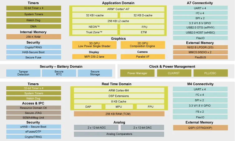
 NXP “With FD-SOI we're enabling the future of embedded processing,” the always-quotable (and keynote speaker) NXP VP/GM Ron Martino told us. NXP's i.MX7ULP, i.MX8, i.MX8X and i.MXRT are all FD-SOI based. They all share fundamental building blocks, so NXP can build platforms, scale and re-use IP. “It's better than any technology I've worked on in my 30 years in the industry,” he said. They're seeing much higher performance with on-chip flash. And the RT “crossover” processor boasts 3x higher computing performance than today's competing MCUs. This is going to be critical for edge computing going forward, to which end NXP is working very closely with foundry partner Samsung. FD-SOI is not just helpful for the logic part of these chips – memory technologies also share in the benefits. They get much higher performance with on-chip flash. Leakage is cut by a factor of ten with biasing techniques, and the enhancements mean that memory can operate at very low voltages. NXP is increasingly sophisticated with how they use body biasing, applying high-granularity techniques to independent domains in different parts of the chips. Getting sub-0.6 Vmin delivers value at multiple levels: on battery life, on total system cost, and on system enablement. Invest in body biasing if you want to get leadership results, advised Martino. 
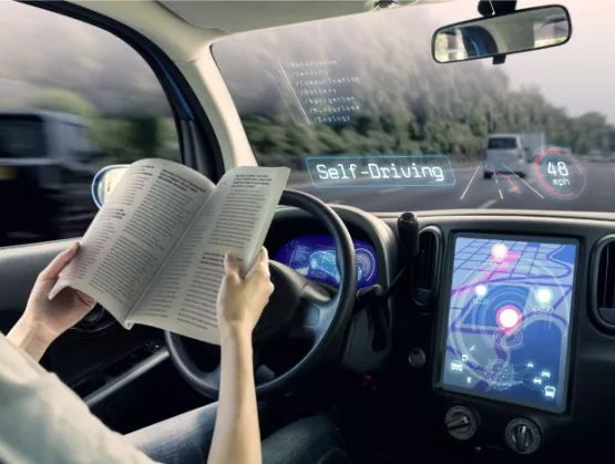
Edge computing – including machine learning and neural networks for things like image classification – is a big target, he continued. At the last CES they did a proof-of-concept “foodnet” where two appliances talked to each other without having to go to the cloud. In that case it was an i.MX8 in a fridge and an i.MXRT in a microwave, but he explained that the same concept can be applied to a car for driver awareness, where you don't want to take the extra time for or don't have a connection to the cloud. iMX and FD-SOI enable scalable solutions, he concluded. Audi What's a metal-bending company doing talking about electrons? asked Audi Project Manager Dr. Andre Blum. And why SOI? Well, for Audi, he said, SOI stands for Solutions, Opportunities and Innovation. [caption id="attachment_11790" align="alignleft" width="300"] Audi Project Manager Andre Blum says SOI stands for Solutions, Opportunities and Innovation -- at the 2018 SOI Symposium in Silicon Valley.[/caption] Audi is working on the various levels of autonomous driving, and they want it to be without design limitations. That means being able to hide sensors wherever they're needed. They'll create a cocoon around the car for the best driver experience. He showed a fun video Audi's made to illustrate their concept – it's the Invisible Man video, which you can check out on YouTube. But those new architectures can't up the power budget (think heat): rather they need to cut power drastically while increasing performance. And with FD-SOI, they see an opportunity to do just that, he said, while integrating the sensors. Audi is one of 25 partners in a heavily funded ( 100 million Euros) brand new EU Horizon 2020 program called Ocean12 (lead by Soitec). The launch was only May 1st 2018 (so as of today it doesn't even have a website yet), and it will run for about 4 years. It is described by ECSEL (a public-private entity that puts together the big EU research projects) as an “opportunity to carry European autonomous driving further with FDSOI technology up to 12nm node”. One to watch! Airbus For Airbus, it's all about increased connectivity and communications that are trusted and secure, said company expert Olivier Notebaert. Since their chip runs are low, NRE – non-recurring engineering costs – are very important; and they need flexible systems. SOI has a long history in aerospace – in fact that's originally where it got its start, since it can handle radiation and is immune to latch-up. Notebaert says that even for Airbus, IoT is their future. The developments they pioneer will be part of it. Airbus is a partner in the EU Horizon 2020 DAHLIA project – which stands for Deep sub-micron microprocessor for spAce rad-Hard appLIcation Asic. The project is, “...developing a Very High Performance microprocessor System on Chip (SoC) based on STMicroelectonics European 28nm FDSOI technology with multi-core ARM processors for real-time applications, eFPGA for flexibility and key European IPs, enabling faster and cost-efficient development of products for multiple space application domains. The performance is expected to be 20 to 40 times the performance of the existing SoC for space.” According to another recent presentation, DAHLIA is prototyping an FPGA this year that will be in production in 2019.
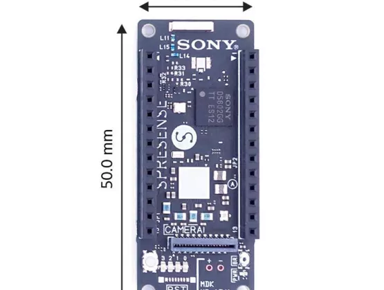
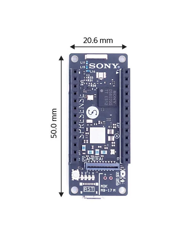
 Sony For Sony GM Kenichi Nakano, FD-SOI has big potential for low-power products. And he should know. Sony has been an FD-SOI pioneer, using it as the basis for GPS chips that are now in a growing number of cool products, especially watches. They're getting good feedback from the market and see good opportunities across a diversified global customer base, he said. Their CXD5603, for example, is the lowest power GNSS (GPS) chip worldwide. In mass production since 2015, it is now dominating world wearable markets like trackers -- such the popular Amazfit line. Running through their various FD-SOI based GPS offerings, he noted that the GPS is a pretty simple chip. But now customers are asking for more, like for it to work in the water (where a GPS typically doesn't). So Sony has partnered with triathalon teams and are seeing good results. With success, of course, comes greater demands: for greater accuracy, for more precise positioning in motion, for increased height accuracy, for even lower power – and Sony is meeting these demands with FD-SOI, in solutions like the new CXD5602. The CXD5602 product configuration covers audio/video/communications: key factors in IoT. A camera version is releasing this summer, as are main and extension boards. An LTE module will be released at the end of 2018. 
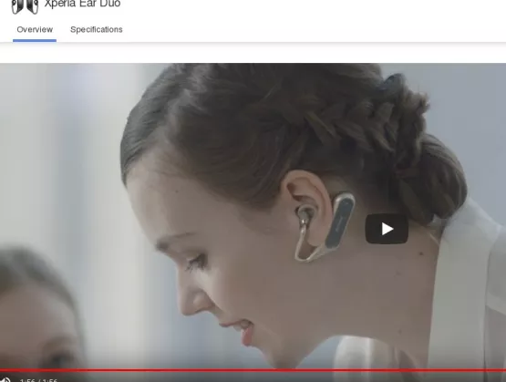
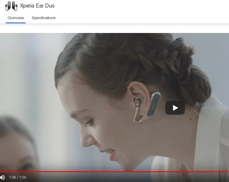
And now they're using those FD-SOI chips in audio applications. You'll find it in the Xperia™ Ear Duo, he said. The MWC press release noted that Xperia Ear Duo “... is driven by Sony’s ultra-low power consuming “CXD5602” chip and a sophisticated multi-sensor platform, the “Daily Assist” feature will recognize time, location and activities to offer relevant information throughout the day – reminding you what time your next meeting is when you reach the office or narrating the latest news headlines.” Also in that PR, Hiroshi Ito,Deputy Head of Smart Product Business Group at Sony Mobile Communications, said, “Ear Duo is the first wireless headset to deliver a breakthrough Dual Listening experience – the ability to hear music and notifications simultaneously with sounds from the world around you.” The highly anticipated wireless “open-ear” stereo headset started rolling out to select markets in Spring 2018. There's a great info page with video here. https://youtu.be/1lKo9acJDPs So that's what we heard in the morning. My next post (or posts?) will cover the afternoon. That includes Dan Hutcheson's excellent talk updating his FD-SOI survey, presentations from Samsung, Globalfoundries and Simgui, plus some from very cool start-ups, and the final panel presentation.
Read More