downloadGroupGroupnoun_press release_995423_000000 copyGroupnoun_Feed_96767_000000Group 19noun_pictures_1817522_000000Member company iconResource item iconStore item iconGroup 19Group 19noun_Photo_2085192_000000 Copynoun_presentation_2096081_000000Group 19Group Copy 7noun_webinar_692730_000000Path
Skip to main content
Default Banner Image

SEMI News

The SEMI Foundation is undertaking a bold, novel approach to ensuring that the semiconductor industry has the skilled talent it needs to thrive. With a $40 million initial award from the U.S. National Science Foundation together with the U.S. Department of Commerce, and up to $160 million additional funds over the next five years, we have launched the National Network for Microelectronics Education (NNME), which is designed to reshape the landscape of microelectronics education and industry career awareness. The NNME is a federal effort to develop, connect and multiply workforce development activities throughout the nation to meet the needs of the semiconductor industry. The SEMI Foundation now serves as the Operating Hub of the NNME and will support large, multi-state regional coalitions of workforce development performers, called Regional Nodes. Collectively, the Hub and the Nodes will work to transform semiconductor industry training and awareness to provide pathways toward economic opportunity for American workers, and to provide industry the workforce it needs to grow to $1 trillion by the early 2030s.Join the NNMEOn July 16, 2025, we will begin accepting Letters of Interest (LOI) from institutions interested in leading or joining a Regional Node. Read on and visit www.nnme.org for more details.The ChallengeThe semiconductor industry has layered workforce development challenges, including: Greying workforce, with 30% of our workers over 50Aging infrastructure and a significant instructor shortageMicroelectronics curriculum that is often outdated and not aligned with industry needs, leading to critical gaps in learner knowledgeNo standardization of microelectronics learning across the fieldDuplicative and disconnected educational efforts nation-wideAn industry largely invisible to many students and jobseekersThe new industry investments spurred by the CHIPS and Science Act mean tremendous economic opportunity for more workers, bolstered American manufacturing, and a stronger U.S. microelectronics sector. None of this can be fully realized without a much larger and highly skilled workforce trained in today’s and tomorrow’s technologies.There have been numerous local, state, and federal workforce development initiatives to address some of these issues, and highly successful programs in various regions; but these have never been connected in a systemic way. This means people and institutions across the country are working separately to solve a collective problem. The NNME will connect and support these efforts, facilitate cross-regional learning, and braid together resources to illuminate the industry to students and jobseekers nationwide.The Solution“Talent is infrastructure,” said Shari Liss, Vice President of Global Workforce Development and Initiatives of SEMI. “We need skilled and job-ready talent at all educational levels to power the semiconductor industry. We have been working for years with educational and workforce leaders to design this national collective effort and we are thrilled to finally launch this transformative work.”The NNME is designed not as a series of isolated interventions, but as a cohesive, forward-looking national strategy. Grounded in the realities of a high-growth industry and an underprepared workforce system, NNME’s goals respond directly to the needs expressed by semiconductor employers, policymakers, educators, and learners. The NNME will:Design, develop, modernize, and disseminate industry-aligned curricula and share best practices across the networkDevelop regional partnerships and local workforce pipelines including colleges, universities, workforce development programs, labor, community-based organizations, and industry to create a national technical workforce that meets the evolving needs of industryFacilitate apprenticeships, internships, and other applied learning experiencesBuild, host, and update an open-source digital portal that houses the updated industry-aligned curricula for adoption in training programs nationwideConduct a major industry awareness, microelectronics education, and career opportunity campaign including PreK-12 schools and STEM organizationsThe NNME will be comprised of the Coordinating Hub (operated by the SEMI Foundation) and Regional Nodes which will be funded by the Hub. Regional Nodes will be comprised of workforce development performers – industry members, academic institutions, training providers, community-based organizations, and more. Collectively, the Hub and Nodes will execute the above activities with a commitment to information sharing and collaboration, transparency, responsiveness and agility, excellence, and accountability. Finally, the NNME is committed to expanding access to microelectronics careers for Americans from every region and walk of life. NNME initiatives are designed to open doors to technical training and career exploration for high school students, veterans, people returning to work, college students, and others seeking high-quality jobs in this critical industry, as well as provide opportunities for current professionals looking to grow their careers. Call for ParticipationThe SEMI Foundation is soliciting LOIs for performers interested in leading or joining a Regional Node. Information on node requirements and performer eligibility can be found on the NNME website at www.nnme.org. The solicitation goes live on Wednesday, July 16. An informational webinar will be held on Wednesday, July 23, and LOIs will be due on Friday, August 8 at 5 p.m. EDT. The NNME envisions a future in which every American, regardless of where they live or how they start their journey, can pursue a rewarding, well-paying career in microelectronics. The NNME will be instrumental in helping to build a robust and vibrant semiconductor industry by fueling it with a wide range of skilled workers and creating a broad pipeline of future talent. Our intention is to serve as the nation's premier resource for microelectronics education and training, connecting learners to employers, programs to successful outcomes, and empowerment to opportunity. We invite industry members and other workforce partners to join us in this work. Together, we will strengthen the talent pipeline that powers American leadership in semiconductors and advanced manufacturing. For more information, contact us at [email protected] or visit www.nnme.org. Michelle Williams is Executive Director at the SEMI Foundation.
Read More
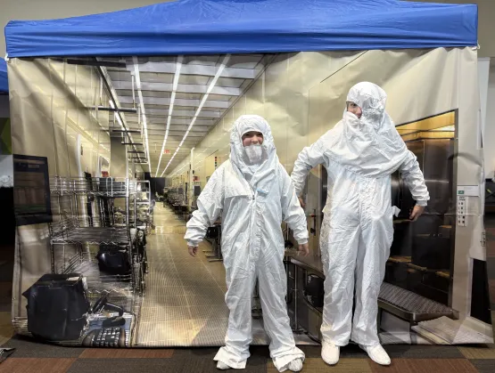
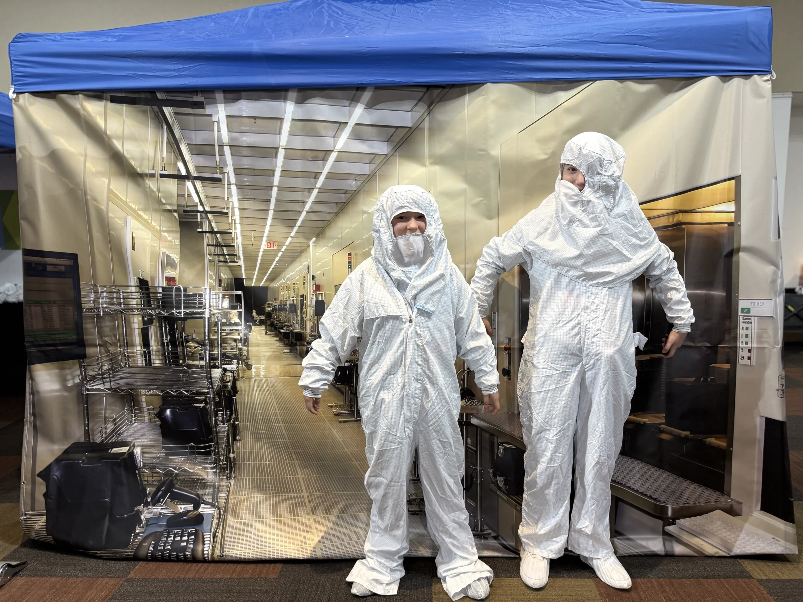
The future of technology depends on cultivating a strong and skilled talent pipeline. According to McKinsey Company, the global semiconductor industry could grow to $1 trillion by 2030, driven by surging demand across sectors like automotive, consumer electronics, AI, and clean energy technologies. That’s why the SEMIquest Pop-Up Exhibition at SEMICON West, October 8-9, 2025 in Phoenix, AZ, will bring the semiconductor story to life through immersive, hands-on learning experiences for students, educators, families, and the general public.What Is SEMIquest? SEMIquest is an engaging, interactive experience designed to introduce students in grades 7-12 to the world of semiconductors. The program features hands-on activities, direct interaction with industry professionals, and workshops for educators aimed at highlighting the essential role semiconductors play in everyday life and future career opportunities. Key Program Components:Students trying on NXP bunny suits at Semiconductor Adventure DayIndustry Engagement – Offering students the opportunity to interact with industry through the interactive exhibition space.Hands-On Activities – Highlighting careers in semiconductors and promoting STEM education for students.Educator Engagement – Offering teachers training and resources to carry lessons back into their classrooms.Field Trip to SEMICON West 2025 – Providing students an opportunity to attend SEMICON West 2025 at the Phoenix Convention Center in Arizona, with complimentary admission and curated tours that offer a behind-the-scenes look at the global semiconductor industry.Students from ASU Preparatory Poly Tech Campus Participating in Semiconductor Adventure Day and event led by the Semi Foundation and ASU PreparatoryThe program culminates in an on-site learning experience at the Arizona Science Center, located adjacent to SEMICON West 2025—where students can explore exhibits, engage with companies, and witness the semiconductor ecosystem firsthand.Projected Reach: In its inaugural year, SEMquest aims to engage 500-1000 students in grades 7-12, with a national expansion plan already in motion.Impact Goal: Reach 60,000 families and students during a 4-month Pop-Up exhibition in Arizona through targeted programming and outreach.Why This Work Matters: The Semiconductor Industry Needs TalentSemiconductors are the foundation of modern life—from smartphones to satellites, healthcare tech to AI applications, and more. Yet, many students are unaware of what semiconductors are or how to pursue a career in the field.The Semiconductor Industry Association (SIA) estimates the U.S. could see a shortfall of 67,000 skilled workers by 2030 in key roles that require postsecondary education.A 2023 Deloitte report warns of a global shortfall of 1 million skilled workers in the semiconductor industry by 2030 if proactive steps aren’t taken.Semiconductor Research Corporation 2023 findings indicate that while 577,000 students pursue four-year STEM degrees annually, only about 19,000 enter the semiconductor industry each year. This disparity underscores a significant gap between STEM education and semiconductor industry employment.SEMI's American Semiconductor Academy (ASA) Vision Paper highlights the importance of raising student awareness through educational and industry collaboration, offering hands-on experiences and real-world applications.Image Source: Photo courtesy of SRC (Semiconductor Research Corporation).The SEMIquest Pop-Up Exhibition tackle this urgent gap through meaningful engagement, accessibility, and experiential learning—helping students envision themselves as future leaders in the field.What Sets SEMIquest ApartReal Industry Involvement – Students interact directly with professionals, tools, and environments used in the field.National Scalability – While beginning in Arizona, the program is structured for national rollout.Cross-Sector Collaboration – A unique fusion of education and industry.Integrated Learning Model – Teachers and students learn together, amplifying classroom impact.Join the Movement: Shape the Future of InnovationWe’re calling on partners across the country to join this work. Whether you’re an industry leader, educator, or community-based organization, your involvement is essential to inspiring and preparing the next generation of innovators.Industry Partners – Showcase your work, engage directly with students, and contribute resources to the traveling Semiconductor Pop-Up Exhibition.Schools Educators – Bring your students, co-host hands-on workshops, and integrate real-world tech experiences into your curriculum.Foundations Funders – Support the expansion of this scalable model and help bring it to communities nationwide.Join us at SEMIQuest! To get involved or learn more, contact Perla DeBaggis at [email protected]. Perla DeBaggis is Sr. Specialist, Career Industry Awareness at the SEMI Foundation.
Read More
On July 7, President Trump issued an executive order (EO) extending the ten percent baseline tariff rate through August 1, 2025. In addition, the EO suspends the variable "reciprocal" tariffs imposed under the International Emergency Economic Powers Act (IEEPA) until August 1. The order applies to nearly all countries except Mexico, Canada, and China. These changes do not impact separate reciprocal tariff actions on China or alter existing Section 232 measures on steel, aluminum, autos, and their derivative products. At the time of this posting, letters had been sent to 20 trading partners outlining expected tariff rates if no agreement is reached by August 1; bilateral negotiations are ongoing. Eleven of the 21 countries received rate cuts compared to the "Liberation Day" announcements on April 2, ranging from one to 13 percent. President Trump indicated rates could rise around 25 percent if trading partners retaliate. Next Steps: The extension offers short-term stability for SEMI member companies to assess supply chain exposure. SEMI continues to monitor bilateral trade and tariff policy negotiations, including for discussion related to the semiconductor supply chain. We aim to keep member companies informed of relevant tariff escalations. If your company is directly impacted by a country-specific rate shift, please reach out to your region’s SEMI Global Advocacy contact with any feedback on how these tariffs are affecting your operations.Visit SEMI Global Advocacy to learn more about public policy efforts and developments as well as how your company or organization can get involved.Scarlett Bickerton, Manager, Federal State Affairs at SEMI.
Read More
In a letter sent to the United States Congress, SEMI, the leading industry association serving the global electronics design and manufacturing supply chain, and 16 member companies urged Congress include in reconciliation an expansion and extension of the Advanced Manufacturing Investment Tax Credit. The letter calls for the expansion of eligibility for the federal investment tax credit (ITC) to make the entire semiconductor manufacturing supply chain, as well as R D and design expenditures eligible for the ITC and extend the credit beyond the current 2026 expiration date—to allow sufficient time to plan and execute investments. The U.S. semiconductor market is growing to meet the needs of critical technology applications like artificial intelligence (AI), telecommunications, and bioengineering that rely on semiconductors. That growth requires increased investment for upstream materials, chemicals, and electronic design automation (EDA), which are currently excluded from receiving the tax credit (also known as Sec. 48D). Excluding these critical manufacturing and R D projects undermines domestic investment efforts potentially ceding U.S. leadership and competitiveness. Semiconductor infrastructure requires billions of dollars in upfront investment, and tax incentives are essential to help offset these exorbitant costs. A competitive tax environment encourages semiconductor companies to invest in the U.S., strengthening domestic manufacturing and innovation while helping the U.S. meet its goals of maintaining global leadership with lower-cost regions also providing incentives.Also, the credit expires at the end of 2026, leaving insufficient planning and implementation time for the billions in upfront investment required to support semiconductor infrastructure in the United States. To support the success, growth, and innovation of the U.S. semiconductor ecosystem, SEMI and its members urge Congress to include in the reconciliation package:Expansion of the Sec. 48D tax credit for the entire supply chain—as included in the SEMI Investment Act (S. 1642)Extension of the credit to allow enough time for businesses to plan and execute needed investments as included in the BASIC Act (H.R. 3204)Recognition of R D and design expenditures as eligible Sec. 48D projects as included in the STAR Act (H.R. 802)These inclusions are crucial to maintain U.S. competitiveness in attracting global semiconductor industry investments.The letter was signed by CEOs or presidents of the following leading companies: SEMI; ASML; ASM; Advantest America, Inc.; Axcelis Technologies Inc.; Brewer Science; Chemours; Dupont’s Electronics business, and Qnity™; Entegris; Evatec NA, Inc.; EFC Gases Advanced Materials; GlobalWafers Co., Ltd.; Lam Research Corporation; Micron Technology; Tokyo Electron America, Inc. TEL Manufacturing and Engineering of America, Inc.; SACHEM, Inc.; SkyWater Technology.Visit SEMI Global Advocacy to learn more about public policy efforts and developments as well as how your company or organization can get involved.Christina Banoub, Senior Manager, Federal Affairs at SEMI.
Read More
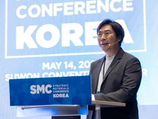
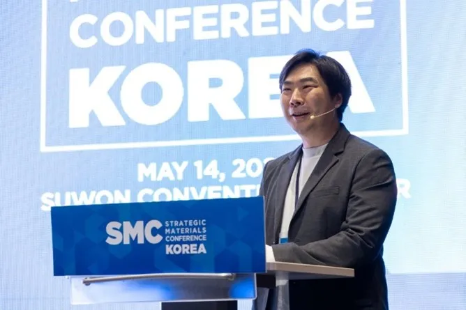
Driven by the recovery of the overall semiconductor market and rising demand for advanced materials for high-performance computing (HPC) and high-bandwidth memory (HBM) manufacturing, global semiconductor materials revenue rose 3.8% year-over-year in 2024. At the heart of this momentum, Strategic Materials Conference (SMC) Korea 2025 brought together approximately 300 industry leaders on May 14 to discuss bold innovation roadmaps and the evolving challenges of the new AI-driven era.Celebrating its 10th edition, SMC Korea served as a convergence point for leaders across the semiconductor ecosystem—including materials suppliers, equipment manufacturers, chipmakers, and academia.“This year’s SMC Korea has recorded the highest level of Q A engagement. A full hour was dedicated solely to an audience-driven panel discussion, where questions ranged from materials technology and business to semiconductor process roadmaps and market outlook. The depth and interactivity of the dialogue reflected the standards of leading technical conferences. Some attendees even noted that it surpassed any academic or industry symposium currently held in Korea,” said Oh Kim, Co-chair of the EMG Korea Chapter and representative of Air Liquide Solutions Korea.Exploring Next-Gen Technologies: 3D DRAM and CFETThe first session focused on next-generation semiconductor technologies, highlighting the future of materials and processes for 3D DRAM and Complementary FET (CFET) devices.Dr. SukKoo Hong, Head of the Material Development team at Samsung Electronics, kicked off the session by outlining a roadmap for materials innovation in 3D DRAM and CFET. Dr. Hong emphasized key technical challenges in the development of 3D DRAM and CFET, highlighting the need for continued innovation in process integration and material engineering. Building on this, Dr. Hong stressed the increasing complexity of material processes and the critical need for tight cross-industry collaboration.Dr. Inhee Lee, Director of imec’s Active Memory Program, highlighted the diminishing improvements in DRAM scaling and emphasized the urgent need for new high-k materials to enable higher density in next-generation 3D DRAM and 4F² DRAM architectures. Dr. Lee emphasized the need for further validation on performance shifts and data retention time resulting from changes in channel materials and architectures.Professor Changhwan Choi of Hanyang University presented key material and process trends for CFET devices, focusing on monolithic and sequential integration as well as Backside Power Delivery Network BSPDN) technologies.The session also featured a presentation by Linghzhi Zhang, Director of Product Management at Air Liquide Advanced Materials focused on “Si, Ge, B Hydrides for Next Generation Semiconductor Devices – Challenges and Perspectives.”The Future of Semiconductor Materials: Market Trends and Innovation StrategiesThe second session highlighted semiconductor materials from multiple perspectives, including market outlooks, advanced technology solutions, and strategic responses to industry challenges.Dr. Prayudi Lianto, Technology Manager at Applied Materials, discussed the technical barriers currently facing HBM, particularly the stacking height limitations. Dr. Lianto highlighted the importance of advanced packaging technologies such as through-silicon via (TSV) and hybrid bonding, and emphasized the critical role of material innovations. Key challenges include void formation during TSV gapfill and developing robust bonding strength and interfacial metals for low-temperature hybrid bonding.Andy Tuan of Linx Consulting provided a market outlook centered on macroeconomic shifts and evolving supply chain structures. Tuan noted that while the semiconductor industry is undergoing a short-term correction, the materials market continues to grow steadily—driven by 300mm logic, DRAM, and 3D NAND. Tuan projected that demand for process materials such as lithography, deposition, and CMP will see a notable recovery post-2025.Dr. Deoksin Kil, Senior Fellow at SK hynix, underscored the growing significance of advanced process materials—including high-performance photoresists, functional chemicals, and CMP slurries—as enablers of semiconductor scaling and 3D evolution. Dr. Kil also stressed the need to maintain consistent quality and supply chain resilience, while pursuing sustainability through low-GWP gases and PFAS-free materials.The session also featured the following presentations:Yohan Ahn, Senior Director, Entegris: “Technological Trends and Necessity of Material Contamination and Filtration for Wafer Defectivity Control in HBM Manufacturing”Dr. Mikko Utriainen, Chipmetrics: “Advancing ALD Tool Qualification Using Ultra-High-Aspect-Ratio Test Structures”SEMI Korea extends its gratitude to all SMC Korea 2025 sponsors for making this insightful conference possible. Dongwoo Fine-chemJSR Electronic Materials KoreaHuntsman Performance ProductsUP ChemicalDuPont Electronics IndustrialDongjin SemichemSK trichemTEMCEntegrisAir Liquide Solutions KoreaJaegwan Shim is Senior Specialist, Marketing at SEMI.
Read More
May is Military Appreciation Month, a time to honor the service and sacrifice of those who’ve worn the uniform — and their families who’ve served alongside them. At SEMI, we believe this recognition must extend beyond appreciation. It should be a commitment to opportunity, support, and action.Through the SEMI VetWorks program, we help transitioning service members, veterans, and military spouses access high-growth careers in the semiconductor and microelectronics industry. We also provide our member companies with the tools and resources they need to successfully recruit, hire, and retain military-connected talent. This Military Appreciation Month, we’re calling on SEMI members to take action — not just in May, but year-round.What SEMI VetWorks OffersVetWorks is more than a program — it’s a network of opportunity that helps bridge the transition from military service to civilian careers. Here’s how we support both job seekers and employers:SEMI VetWorks Guide for EmployersThis guide helps companies understand military experience, translate skills, and develop inclusive hiring strategies that resonate with veterans and military spouses.Monthly Military Resume ReleasesEach month, SEMI VetWorks distributes a curated list of resumes from transitioning service members and military spouses to participating member companies. This direct pipeline provides early access to mission-ready talent.Perla DeBaggis and Melinda Gomez of the SEMI Foundation at Luke AFB Military Hiring EventMilitary Engagement EventsVetWorks hosts and joins industry-specific hiring events, career fairs, and workforce development briefings that connect member companies directly with military-affiliated candidates.careers.semi.org/militaryThis dedicated career portal is designed for veterans and spouses exploring semiconductor industry jobs. It features training resources, employer spotlights, and a streamlined job search experience tailored to the military community.Our Strategic PartnershipsVetWorks also partners with organizations that share our mission to support veterans and military spouses. Together, we provide critical services, from career coaching to job placement and certification programs. These include:Department of Labor’s Employment Navigator Partnership Program (ENPP)We work closely with DOL Navigators who refer transitioning service members to SEMI for career coaching and connection to job opportunities.Marvin Branch of Heroes MAKE America, Melinda Gomez of SEMI VetWorks and Eric Putt of Hiring Our Heroes at Ft Cavazos Semiconductor Information Session Hiring Our Heroes (U.S. Chamber of Commerce Foundation)A national initiative that SEMI VetWorks supports through event participation and career pathway promotion in the semiconductor industry.Heroes MAKE America (Manufacturing Institute)Prepares veterans for advanced manufacturing roles with hands-on training, certifications, and job placement support.NYCREATES Vet S.T.E.P.A New York-based program offering veterans specialized training and certifications for semiconductor manufacturing roles.DOD Military Spouse Employment Partnership (MSEP)Connects military spouses with employment opportunities that offer flexibility and long-term career growth.What SEMI Members Can Do NowSupporting the military community is not only the right thing to do — it’s a strategic investment in a dedicated, adaptable, and highly skilled workforce. Here are five actionable ways your company can get involved:Use the VetWorks Guide to educate HR and hiring managers on how to evaluate military experience.Sign up for our Monthly Resume Release to receive vetted candidates directly from our pipeline.Participate in Military Engagement Events to connect with transitioning service members and spouses.Establish internal support systems, such as military-affiliated Employee Resource Groups (ERGs) or mentorship programs.Review and adjust your benefits policies to better support reservists, National Guard members, and military families (e.g., flexible leave, relocation support, remote work options).These actions not only improve veteran and spouse recruitment — they strengthen your organization’s culture, resilience, and brand reputation.Join Us in Building the FutureThis Military Appreciation Month, we honor those who have served by building pathways for them to thrive in our industry. Through SEMI VetWorks, we’re proud to create those pathways — but we can’t do it without you.Get started today:Visit semi.org/veteransExplore our military to semi careers portalReach out to Melinda Gomez ([email protected]) with the SEMI VetWorks team to learn how your company can get involvedLet’s turn appreciation into action — and build a stronger, more inclusive industry together.Melinda Gomez is Program Manager, Veteran Initiatives at the SEMI Foundation.
Read More
The semiconductor industry is at the heart of modern technology, powering everything from smartphones and medical devices to communication systems and transportation. However, to sustain its rapid growth and innovation, the industry faces a pressing challenge: a growing talent gap. Addressing this issue requires collaboration between academia and industry to ensure that students are not only equipped with the necessary skills but also have clear pathways into the workforce.That’s where SEMI On Campus comes in. Launched in March 2025 by SEMI Europe, this new initiative is designed to bring together the semiconductor industry and universities, fostering collaboration that benefits students, educational institutions, and companies alike. With its first edition in Poland, SEMI On Campus is already making waves by reaching over 150 students and strengthening industry-academia connections.First Stop: PolandThe inaugural SEMI On Campus event took place at Gdańsk University of Technology and The University of Gdańsk, where key representatives from SEMI Europe—Bernard Capraro (Senior Manager, University Partnerships Talent Initiative), Victoria Cummings (Senior Manager, Workforce Development EU Projects), Maria Daniela Perez (Senior Manager, Business Development), and Kartikey Srivastava (Senior Specialist, Communications)—met with deans, professors, and students from various faculties.The Power of Industry-Academia CollaborationCollaboration between universities and the semiconductor industry is crucial in ensuring students gain practical knowledge, hands-on experience, and direct access to job opportunities. Companies, in turn, benefit from a steady pipeline of skilled graduates ready to drive innovation and meet industry demands.During the event, Bernard Capraro shared his own journey, from an engineering internship in Germany to leading research and development initiatives at Intel. His experience highlighted how diverse skill sets and career paths can lead to impactful roles in the semiconductor industry."Yes, the industry needs mechatronics engineers, data scientists, chemists, physicists, and computer science professionals. But it also needs media experts, gamers, biologists, environmentalists, public policy professionals, and communicators. It’s all about transferable skills and finding your area in this dynamic and diverse industry,” said Capraro.Expanding Opportunities with the European Chips Skills AcademyOne of the key initiatives supporting the semiconductor industry’s workforce development is the European Chips Skills Academy (ECSA). Designed to tackle skills shortages and propel industry growth, the Academy builds on the goals of the Microelectronics Pact for Skills and the EU Chips Act. With backing from 18 partners, including vocational training providers, research organizations, and industry leaders, ECSA aims to:Attract new talent into microelectronicsFoster collaboration between educational institutions and industryProvide training and certification opportunities to enhance workforce readinessVictoria Cummings emphasized how the initiative offers mentorship programs and access to leading companies and events. ECSA also builds on the student ambassador initiative, empowering institutions to support students in developing ideas and connecting them with mentors who can help shape their careers.Driving Diversity with the European Chips Diversity AllianceDiversity, equity, and inclusion are key to strengthening the semiconductor workforce. Kartikey Srivastava highlighted the European Chips Diversity Alliance (ECDA), a collaborative effort between academia and industry that aims to lower barriers to participation for underrepresented groups.With 11 partner organizations, the ECDA seeks to enhance inclusivity in the microelectronics sector, ensuring that the industry remains competitive and accessible to all. By fostering inclusive talent pipelines, the initiative is helping shape a more equitable and innovative future.A Successful Launch with a Bright FutureThe first SEMI On Campus event was a tremendous success, not only for the students who gained valuable insights and networking opportunities but also for universities and industry leaders looking to strengthen their collaboration. By building bridges between academia and industry, SEMI On Campus is paving the way for a more skilled and dynamic semiconductor workforce in Europe.If you’re interested in hosting a SEMI On Campus initiative or inviting an industry representative to speak at your institution, please reach out to [email protected]. Let’s work together to inspire the next generation of semiconductor leaders!SEMI Contact: Maria Daniela Perez, Senior Manager Business DevelopmentEmail: [email protected] Lam, Manager Business DevelopmentEmail: [email protected]
Read More
The new Administration in the United States has been aggressively focusing on trade measures to establish more balanced relationships with its trading partners, according to the White House.Over the last several weeks, President Trump declared a U.S. economic emergency and announced a universal 10% tariff on all countries, which went into effect on April 5, 2025. There are also levies that Trump has called “reciprocal,” including a 34% tariff on Chinese goods and a 20% tariff on European Union imports, that started on April 9.Previously announced 25% tariffs on foreign-made autos and certain auto parts are also now in effect.Presently, finished semiconductors are exempt from these tariffs, however, a Federal Register notice provided the following update:On April 1, the Secretary of Commerce initiated an investigation under section 232 of the Trade Expansion Act (19 U.S.C. 1862) to determine the effects on national security of imports of semiconductors, semiconductor manufacturing equipment (SME), and their derivative products. This includes, among other things, semiconductor substrates and bare wafers, legacy chips, leading-edge chips, microelectronics, and SME components. Derivative products include downstream products that contain semiconductors, such as those that make up the electronics supply chain. The SEMI Advocacy team is working side by side with member companies in the U.S. to prepare industry’s response for the public comment period tied to the 232 investigation. Comments are due May 7. (Update: SEMI comments submitted.)SEMI has been tirelessly working to educate new policymakers and regulators about the negative impacts the proposed tariffs have on the semiconductor industry. Ajit Manocha, President and CEO of SEMI, and Joe Stockunas, President of SEMI Americas, have been to Washington, D.C. for a series of meetings with administration officials and on Capitol Hill. Clarity on the recent tariff announcements — and guidance on what could come next — has been at the top of the agenda. Additionally, many member company executives recently attended the SEMI Washington Fly-In to advocate for policies that support the global supply chain on Capitol Hill, and the topic of tariffs was of the highest priority for congressional staff.Considering the complexities of the semiconductor industry supply chain, U.S. companies must rely on highly specialized materials, equipment, and components sourced from multiple countries. Strategically deployed and comprehensively assessed trade actions ensure that U.S. businesses maintain market access to critical supplies and remain globally competitive.Additionally, SEMI has highlighted that through fair and reciprocal trade practices, the U.S. can avoid unintended cost increases, supply chain disruptions, and ultimately any risks to American competitiveness in the global marketplace. Coordinating trade policies with allies prevents retaliatory tariffs for industries critical for national security, such as the semiconductor industry, and keeps costs competitive for consumers and industries, all while fostering a more resilient domestic manufacturing ecosystem. Semiconductor companies make substantial investments in building new facilities, and policy stability and predictability are key factors in site selections. With governments around the world putting incentives in place to bolster their semiconductor ecosystems, and to attract industry investments and good-paying jobs, public-private synchronization on trade policies is crucial to help the U.S. meet its technology innovation goals.Visit SEMI Global Advocacy to learn more about public policy efforts and developments as well as how your company or organization can get involved.John Cooney is VP, Global Advocacy Public Policy at SEMI.
Read More
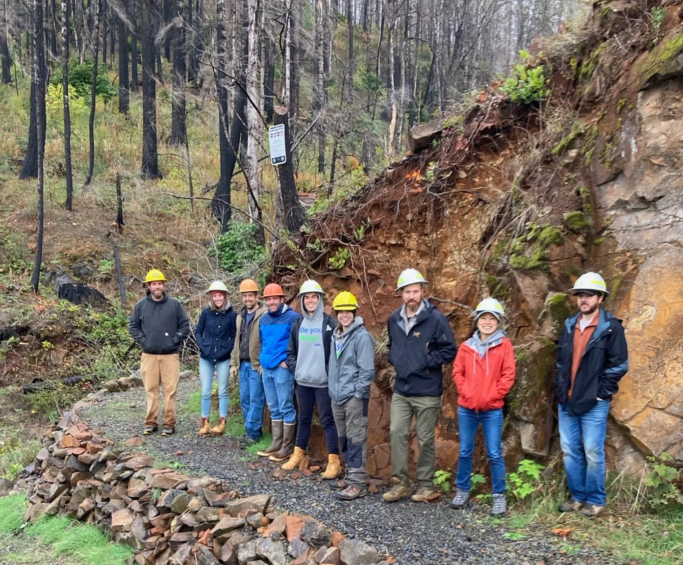
Gregory Woods, leader of the San Diego-based Green ASML employee group, stands with the tree-planting team at the Santiam State Forest site in Oregon, October 2023.Photo Credit: Dave Laegen, veritreeA tree-planter is geared up for a day of restoration, a result of the public-private partnership with American Forests and the Oregon Department of Forestry.https://veritree.mediavalet.com/portals/OregonOverviewForests hold the natural world together…. They are the ecosystem engineers that create the conditions for other forms of life to exist, on every level.— Jim Robbins, “The Man Who Planted Trees”Climate-driven events like fire and smoke events are becoming increasingly common along the Pacific coast, from British Columbia to California. In the wake of the 2020 “Labor Day” wildfires that devastated large parts of Oregon, a US employee network group at ASML, a leading player in the semiconductor industry, sought an innovative way to contribute to restoring the environment and sequester carbon. This commitment led to a partnership with veritree, a technology-driven reforestation organization, resulting in a groundbreaking initiative — starting with 40,000 trees.The ChallengeDuring an interview for this story, Markus Matthes, former Site Lead at ASML San Diego, current Head of ASML Germany and Chairman of the Berlin Management Team and sponsor of the local employee-led network, noted that in light of the semiconductor industry’s energy consumption and chemical inputs, “I was pleased to support this proactive approach from the local employee network group. At ASML, we feel it is important to play our part in addressing key environmental and social concerns that we share with our stakeholders.” Over the last 3-5 years, companies in the semiconductor value chain have strived to collaboratively identify critical steps on the path to net zero emissions through industry alliances like the SEMI Climate Consortium.Green ASML San Diego, an employee network group (ENG) led by Gregory Woods, Senior Systems Industrialisation Engineer and Chair of Green ASML San Diego, decided a proactive approach to giving back could be to help restore the forests that Oregon lost 4 years ago. But they wanted to make a meaningful environmental impact, ensuring transparency and accountability while also advancing carbon sequestration efforts. With reforestation as the focus, the challenge was identifying a partner capable of delivering measurable, long-term results while providing visibility into the process. This was a sticking point for Matthes, who affirmed that “we do not want to do window dressing in terms of planting trees … we also want to have evidence that it’s really working, that trees are really growing, that they are storing CO2, etc.”The SolutionThe idea to plant ‘one tree per employee’ began with Woods and Green ASML San Diego before quickly gaining executive sponsorship. Matthes expressed pride in the San Diego Green Team and attributed the success of the program to their persistence. Where he and Martin Reinecke, Head of Cymer Business Planning and Operations, Cymer Light Sources San Diego, came into play as the executive sponsors in guiding how to get the project funded: “typically we know the folks in the headquarters. We know how to approach them. And then we can also perhaps help in making a catchy story.”More than just a catchy story, partnering with veritree made for a sound pitch. They stood out among other reforestation providers due to their innovative assemblage of GIS, blockchain, and sensor technologies. This approach ensures every tree planted is verified, monitored, and accounted for over time. With support from ASML’s leadership, Green ASML San Diego partnered with veritree to restore 40,000 trees — one per each of ASML’s 40,000 employees — to an area near ASML Hillsboro, that was heavily impacted by Oregon’s Labor Day fires.By leveraging this technology, veritree provides real-time updates on the health of the ASML forest and its long-term project outcomes. ASML has benefitted from access to real-time project data, which have reinforced trust and engagement among stakeholders while setting a high standard for nature-based carbon removal projects. As Matthes put it, “here Mother Nature is doing most of the work. We are just observing and checking ... we really have evidence that it’s really doing something good.”ResultsThis partnership is not only bringing back life to the fire-damaged landscape but also demonstrates how technology can enhance transparency in environmental initiatives. For SEMI companies with similar aspirations, Matthes highlighted one benefit of supporting ENGs is that their success “radiates back into the organization itself.” He said initiatives like this act as an “intrinsic motivator.” Woods added that it creates a positive sentiment within the company that “ENGs with the right ideas, with the right enthusiasm ... can actually make a difference.”Through their collaboration with veritree, Green ASML San Diego turned a spark of inspiration into a powerful movement, offering a replicable model for other corporations. To achieve these results, Matthes recommended that fellow SEMI companies should “trust your ENG” and “try to place it … as a combination of a grassroots initiative with some strong executive support.” Starting with a simple ‘one tree per employee’ concept, ASML was able to scale the idea into a significant environmental initiative. With Woods’ vision of growing the ASML forest from 40,000 to 3 million trees over the next few years, the movement continues.Key Project MetricsAll data related to the trees is accessible via ASML’s Impact Hub2 public partners: Oregon Department of Forestry and American Forests40,000 trees planted: Douglas-fir, Noble Fir, Western Red CedarCarbon sequestration: 23.1k tons of CO2 over lifetime of treesEcological impact: 26.68 hectares restoredEconomic impact: 160 work days provided“The How”: Recommended action steps for achieving broad buy-inCarbon removal highlighted as a focus area for Green ASML San Diego throughout 2022Green ASML (Employee Network/Resource Group) met with potential partner veritree to learn about planting methodology, sites and how to start partnershipGreen ASML San Diego chapter presents the project to local executive sponsors and global Green ASML sponsor (ASML Executive Committee member). Received unwavering support to move forward and “ASML pledges to plant 40,000 trees for holiday season ’22, planting one tree for every employee and celebrating its drive to pioneer sustainable semiconductor manufacturing.”Post-fire restoration project in Oregon, USA chosen as planting site for local community engagement (ASML Hillsboro and Intel Corporation)Memorandum of Understanding (MOU) signed by ASML Procurement team and veritree in Oct-Nov 2022In April 2023, the 40,000 trees were allocated to ASML from a 200,000 initial planting roundRestoration initiative recommended to be communicated as US-driven project, instead of a global ESG initiative, since it did not meet certain carbon offsetting criteriaImpact data, GPS coordinates and field reports (Survivability Assessment) provided for verification from veritreeGreen ASML San Diego board visited Oregon planting site with veritree team, American Forests (NGO) and Oregon Department of Forestry in Oct. 2023Impact Hub showcases ~716.10 tons of CO2 sequestered from year 1 (Dec. 31, 2023)Green ASML continued prioritization towards restoration/reforestation projects throughout 2024 and how to expand with veritreeIn 2024, an additional 7,452 trees were funded to be planted in Oregon, USA plus 5,000 mangrove trees were funded in KenyaAbout the Author:Nat Mengist is a PhD student in Learning Sciences at the University of Washington. He recently earned a master’s degree in Human Centered Design and Engineering and he serves on the executive board of the Society for Literature, Science, and the Arts. As a storyteller, Nat has created multimedia science fiction about the future of climate justice. This article was a team effort, written on behalf of veritree and the SEMI Sustainability Initiative.
Read More
On April 8-9, 2025, bees on cherry blossoms lining the streets of Washington D.C. were not the only things buzzing. The word “tariffs” floated in the air from TVs and conversations throughout Capitol Hill, as people eagerly awaited the implementation and response to United States President Donald Trump’s latest round of far-reaching trade policy. This was the backdrop for this year’s SEMI Washington Fly-In, hosted annually by the SEMI North America Advisory Board (NAAB), which gathered representatives from member companies to meet with government officials and advocate for policy changes vital to the semiconductor industry’s continued growth and innovation.SEMI executives and more than 50 representatives from member companies across the end-to-end semiconductor supply chain participated in the Fly-In. SEMI President and CEO Ajit Manocha, SEMI Americas President Joe Stockunas, and SEMI Vice President of Global Advocacy and Public Policy John Cooney met with Trump administration officials from the Department of Commerce. Reflecting the global reach of SEMI, Manocha traveled from Washington to Brussels for meetings with the European Commission. On April 8, Stockunas presided over a NAAB meeting, followed by a dinner and prep session for meetings with Congressional members and their staff the following day. Building on the priorities outlined in the briefing book prepared by Cooney’s Advocacy team in Washington, participants discussed priority messages to convey tailored to the specific officials.Focus topics included:Tariffs and Trade – Address the buzz of the day’s news cycle by spotlighting the challenges of multiple layers of tariffs facing U.S. operations due to the industry’s global supply chain.Export Control Policy – Revise export control rules to be narrow and focused with increased transparency to minimize uncertainty for companies contributing to the world’s most complex manufacturing processes.Tax Policy and Investment Incentives – Extend tax credits set to expire and expand them to include semiconductor material suppliers and packaging facilities to bolster the full semiconductor ecosystem.CHIPS Act Implementation – Streamline implementation and ensure that the full intended scope of the CHIPS Act is maintained to meet the goals of the bipartisan legislation.Workforce Development and Immigration – Highlight the need for multi-layered programs – from education to apprenticeships through career development – required to provide the skilled workforce that will underpin domestic industry expansion.Energy and Environment – Showcase the need for strong R D programs, industry-led standards, and permitting reforms to help the semiconductor industry address booming energy requirements to power Artificial Intelligence and meet the resource needs of the growing domestic chipmaking ecosystem.PFAS Regulation and R D Needs – Prioritize regulatory actions that take a risk-based approach to PFAS and other chemicals critical to semiconductor manufacturing, as well as R D to improve environmental controls and identify potential alternative substances.SEMI organized four groups by U.S. region – East, Midwest/South, Southwest and West – comprised of representatives from member companies with operations in the respective states of the Senate and House of Representative offices scheduled for meetings at Capitol Hill. On April 9, the groups met with Members of Congress and their staff from 20 of the nation’s states, including Arizona, Arkansas, California, Colorado, Delaware, Idaho, Kentucky, Louisiana, Massachusetts, Michigan, Minnesota, New Mexico, North Carolina, Ohio, Oregon, Texas, Utah, Virgina, Washington and West Virginia. The groups shared powerful perspectives, data and anecdotes on the impact of policies on their companies’ operations. While the groups for the SEMI Washington Fly-In included representatives from companies that are fierce business rivals, the focus of the discussions successfully presented a unified industry voice highlighting shared challenges, policy recommendations, and request for support – in true SEMI “Stronger Together” spirit.News of a 90-day pause on most tariffs broke while the groups were conducting their meetings. The intense difficulties of tracking changes on tariffs and other policies permeated throughout the conversations on the impact on business decision-making. While influencing policy changes will not occur instantaneously, the SEMI Washington Fly-In bolstered the SEMI Global Advocacy team’s ongoing efforts to educate officials on the nuances and critical importance of the complete semiconductor supply chain. Additionally, the discussions emphasized the policy modifications that will have the greatest impact in helping the industry continue its lasting legacy of innovation that improves the quality of life for people in the U.S. and around the world.On April 11, the Customs and Border Patrol issued an addendum to the tariff exemption list that did not result in a complete exemption for the semiconductor supply chain. President Trump posted afterward on social media: "We are taking a look at Semiconductors and the WHOLE ELECTRONICS SUPPLY CHAIN in the upcoming National Security Tariff Investigations."Traditionally, such investigations have been conducted over a prolonged period of time for the government to collect data directly from companies and solicit feedback from industry. If past precedent remains, this will represent the first formal opportunity for industry to engage on the Administration's tariffs. The President has stated that his plans for tariffs on semiconductors will be unveiled this week.Visit SEMI Global Advocacy to learn more about public policy efforts and developments, and SEMI Workforce Development for more information on efforts to address the microelectronics industry’s talent needs.Samer Bahou is Director of Marketing Communications at SEMI.
Read More