downloadGroupGroupnoun_press release_995423_000000 copyGroupnoun_Feed_96767_000000Group 19noun_pictures_1817522_000000Member company iconResource item iconStore item iconGroup 19Group 19noun_Photo_2085192_000000 Copynoun_presentation_2096081_000000Group 19Group Copy 7noun_webinar_692730_000000Path
Skip to main content
Default Banner Image

SEMI News

The Rising Stars: 20 Under 30 blog series celebrates the brightest young leaders shaping the future of the semiconductor industry. These exceptional individuals have earned the SEMI Europe 20 Under 30 Award for making a remarkable impact across the supply chain—whether in engineering, sales, marketing, or R D. Nominations for the 2025 20 Under 30 Award are now open, providing the opportunity to recognize and honor the next wave of industry trailblazers.The series spotlights these rising stars for their career achievements, commitment to innovation, leadership skills, and dedication to driving both business success and community growth.Follow their inspiring journeys and discover how they are thriving and paving the way for future generations in the semiconductor world.Meet Eloise Bond, Senior Etch Process Engineer at KLA Corporation (SPTS Division)Eloise Bond studied Physics at Swansea University before joining KLA in 2019 as an Etch Process Engineer. Since then, she has worked on cutting-edge semiconductor applications while actively promoting STEM through local outreach programs like Generation Tech.A proud recipient of the SEMI Europe 20 Under 30 Award, Bond shares how the recognition boosted her confidence and expanded her network, enabling her to take on new challenges. In her interview, she reflects on overcoming imposter syndrome, the value of flexible work, and the unexpected opportunities that shaped her career. Outside of work, Bond enjoys camping and bouldering.SEMI: What inspired you to join the semiconductor industry? Bond: I’ve always had a passion for science, so pursuing a career in a related field was natural. However, I wasn’t aware of the semiconductor industry until I began studying Physics at Swansea University, which has strong research ties with local semiconductor companies like KLA. Now that I am in the industry, I enjoy the hands-on aspects of my job. I find working with different materials and equipment is more engaging to me than an office-based job. SEMI: How did your early experiences and education shape your career path?Bond: STEM activities during my childhood and visits to museums with my parents sparked my interest in science and the physical world. That curiosity lead me to study physics at Swansea University, which ultimately paved the way to my current role at KLA. As I mentioned earlier, a career in semiconductors wasn’t really a conscious choice until relatively late in my education; I simply followed my passion for science. Today, I’m involved in many of the STEM outreach programs at KLA, helping to promote the semiconductor industry to young children so they can discover the same opportunities that I was fortunate to have had exposure to earlier in my life.SEMI: Can you share a professional accomplishment you’re most proud of, and explain why it’s significant to you?Bond: One accomplishment I’m particularly proud of is building strong customer relationships with a volume production fab in Korea. It was my first experience with direct customer interactions, which felt quite daunting at the time. I was invited to support a tool installation on-site, which allowed me to travel the furthest from the UK I had ever gone. Seeing firsthand how our tools fit into the wider industry gave me valuable context for my day-to-day responsibilities and made my work feel even more impactful. SEMI: As a young professional in the industry, what is your greatest challenge? Bond: Imposter syndrome has been a significant challenge for me. I often find myself in meetings with more senior colleagues and fear I am not performing well enough. However, over time, I have learned that my input is valid and that having multiple perspectives often leads to better outcomes.SEMI: What advice would you give to younger generations aspiring to make an impact in this industry?Bond: To make a difference, you first need to be part of the industry, just getting involved puts you in the room where conversations and decisions happen that you might not otherwise be exposed to.If an opportunity comes your way, take it. I entered this industry due to an opportunity presented to me at the end of my university career. KLA was my first real interview, and I honestly thought my chances were slim. I approached it as a ‘trial run’ and five years later, I’m still here. SEMI: How do you envision future work environments?Bond: I envision a new generation of management that places greater value on work-life balance. In many industries, senior management seem to have a relatively poor work-life balance, such as constantly doing business in the same way they’ve done for the past 40+ years – with constant business travel, working on holidays and long hours in the office. There is still an expectation for younger, ambitious employees to emulate this corporate culture, which creates barriers for those with caregiving responsibilities or other important commitments outside work. I believe a younger, more vocal generation of managers will drive positive changes in how we work. We will see more adoption of fully flexible working and 4-day weeks – happy employees lead to better work outcomes. I also think the technological advances which enabled the rapid switch to “working from home” during the COVID pandemic have permanently reshaped what is possible in terms of flexibly and efficiently.SEMI: What impact has the 20 Under 30 Award had on your career? Bond: This award has given me greater confidence to step outside of my comfort zone. It has also allowed me to increase my network to include colleagues I would have no reason to speak to previously. As a result, I have gained broader knowledge of how KLA operates as a whole and have been able to initiate small cross departmental projects I would not have been possible to before. Following 20 Under 30 JourneysEloise Bond’s journey highlights the passion, resilience, and forward-thinking mindset that characterize today’s emerging leaders in semiconductors. Her dedication to both technical excellence and community engagement showcases how rising stars are not only advancing the industry but also inspiring the next generation.The Rising Stars: 20 Under 30 blog series celebrates the exceptional talent and leadership driving the future of the semiconductor industry. Each of the young innovators honored is excelling in their respective fields while shaping the landscape of technology and business with their visionary approaches and dedication. Their stories exemplify the remarkable achievements and unwavering commitment that define the next generation of industry leaders. The series is intended to inspire and motivate future professionals to pursue their passions and embrace the opportunities within this dynamic industry. Stay tuned for more stories of rising stars who are paving the way for continued growth and innovation in the semiconductor world.Learn more about the SEMI Europe 20 Under 30 Award and the recipients honored at SEMICON Europa. SEMI ContactMaria Daniela Perez, Communications ManagerEmail: [email protected]
Read More
Every November, the U.S. pauses to honor those who have served our nation—the men and women whose dedication, discipline, and teamwork have safeguarded our freedom. The best way to thank veterans is not just with words. It’s with action.In the semiconductor industry, that action means creating pathways for veterans to build meaningful civilian careers where their skills, experience, and values are not only recognized, but celebrated. Through SEMI Foundation’s VetWorks initiative, companies across the industry are doing just that, working together to raise awareness, share best practices, and open doors for the military community.Through VetWorks, SEMI is proud to help veterans find new purpose in powering the technologies of tomorrow. And as more employers recognize the unmatched value of veteran talent, the industry will continue to grow stronger technically, strategically, and culturally.Why Veterans and Semiconductors Are a Natural MatchVeterans bring the kind of precision, accountability, and technical excellence that drive the semiconductor industry forward. From operating complex systems to leading diverse teams under pressure, veterans possess the same qualities that make this industry thrive.Kathy Garner, Director of Talent Acquisition at TEL (Tokyo Electron), notes:“Veterans are well-versed in cutting-edge technology. Today’s military is high-tech, state-of-the-art, and computer-based. Veterans are uniquely matched to our industry as their jobs are highly technical and safety-conscious; they appreciate guidelines, follow directions, and possess a strong sense of team.”This alignment of skills and culture makes veterans not just excellent employees, but invaluable contributors to the semiconductor industry’s mission of powering innovation and national competitiveness.Turning Appreciation into OpportunityAcross the VetWorks Employer Group, companies are transforming gratitude into action by recruiting, training, and supporting veterans and reservists as they transition to civilian careers.“I participate in VetWorks because I believe the brave men and women of our military deserve support and opportunities if they choose to enter the civilian workforce,” said Katie Maloney, Business Line Manager at Edwards Vacuum. “They have sacrificed for our country, and we can help connect them to a rewarding career in the semiconductor industry. This transition is often stressful for military members and their families, despite the fact that veterans are ideally suited for the many roles our industry needs to fill. As a Navy veteran, participation is a small way for me to pay it forward.”“The semiconductor industry is full of veterans,” said Curtis Geroy, Manager of Military Talent Acquisition at Applied Materials and a U.S. Navy Reserve Officer. “Serving as a reservist and having leaders who understand my commitment to duty gives me the extra support needed to meet my reserve obligations.”These stories reflect what’s possible when companies don’t just honor veterans but invest in helping them translate their service into purposeful, future-ready careers.An Industry-Wide EffortMany leading employers are already stepping up and partnering through SEMI VetWorks, including Applied Materials, ASM, ASML, Edwards Vacuum, EMD Electronics, Entegris, KLA, Lam Research, Micron, Polar Semiconductor, TEL, TSMC, and Western Digital, among others.Together, they form a growing network of organizations committed to building awareness within the military community, connecting veterans to open roles, and ensuring every company in the semiconductor ecosystem is ready to support them.Through joint events, outreach to bases, storytelling, and shared best practices, the VetWorks Employer Group is showing that this isn’t just a workforce initiative, it’s a movement to strengthen the entire industry while honoring those who have served.Join the EffortThis Veterans Day, let’s remember: saying “thank you” is important, but hiring, supporting, and championing veterans is even more meaningful.If your company is looking to start or grow its veteran hiring and support programs, SEMI VetWorks can help you connect with partners, share resources, and build sustainable pathways for veterans into your workforce. Download the Employer’s Guide to Military Hiring, learn more and get involved in the SEMI VetWorks initiative. Melinda Gomez is Manager of Military Initiatives at the SEMI Foundation.
Read More
SEMI has submitted comments to the U.S. Department of Commerce’s Bureau of Industry and Security (BIS) in response to its Section 232 National Security Investigation of Imports of Robotics and Industrial Machinery.The submission highlights the vital role robotics and precision machinery play in semiconductor fabrication, packaging, and inspection and emphasizes the need for a balanced, risk-based approach to any future trade actions that strengthen U.S. national security while preserving access to robotics and industrial machinery essential to expanding the domestic semiconductor industry. SEMI RecommendationsSEMI outlined five key recommendations to the Administration.Encourage Investment and Maintain Existing Competitiveness. SEMI recommends excluding essential robotics and industrial machinery where domestic sourcing is not yet viable. If trade actions are taken following the investigation, SEMI recommends providing tariff reductions or waivers for companies investing in U.S. manufacturing capacity. SEMI emphasized protecting small and medium suppliers that keep the ecosystem running.Avoid Stacking Tariffs. Coordinate Section 232 actions across potentially overlapping actions and ongoing investigations, such as on imports of steel and aluminum, semiconductors, critical minerals, and polysilicon. This will help prevent duplicative or compounding tariffs that could raise costs and slow U.S. capacity building.Implement Adjustment Periods and Sunset Provisions. SEMI recommends any trade actions should phase in gradually to allow for domestic adaptation and include regular review mechanisms to recalibrate as the market evolves.Pair Trade Actions With R D, Workforce, and U.S.-Allied Collaboration. Strengthen domestic capacity through targeted federal research and development (R D) programs, workforce training, and deeper partnerships with trusted U.S. allies to build resilient technology ecosystems.Develop a National Robotics Strategy. Given robotics’ foundational role across semiconductor and advanced manufacturing sectors, SEMI recommends that the Administration develop a National Robotics Strategy. The strategy should align federal programs including those at NIST, NSF, and Department of Energy to accelerate robotics innovation, update technical standards, and drive U.S. leadership in automation and manufacturing competitiveness.The Global ContextWorldwide installations of industrial robots surpassed 540,000 units in 2023, with the market projected to exceed $73 billion in 2025.Robotics and industrial machinery are integral to semiconductor production ensuring cleanroom integrity, precision, and throughput. Broad or overlapping tariffs could raise costs and undermine U.S. competitiveness at a time when historic investments in domestic semiconductor manufacturing are taking hold.Next StepsSEMI looks forward to working with the Department of Commerce and other federal partners to ensure that Section 232 policies enhance both U.S. national security and the industry’s global competitiveness.Read SEMI’s full submission on Regulations.gov by searching Section 232 Investigation of Imports of Robotics and Industrial Machinery (XRIN 0694-XC138).Visit SEMI Global Advocacy to learn more about public policy efforts and developments as well as how your company or organization can get involved.Marc Coldiron is Director, Global Public Policy Advocacy at SEMI.
Read More
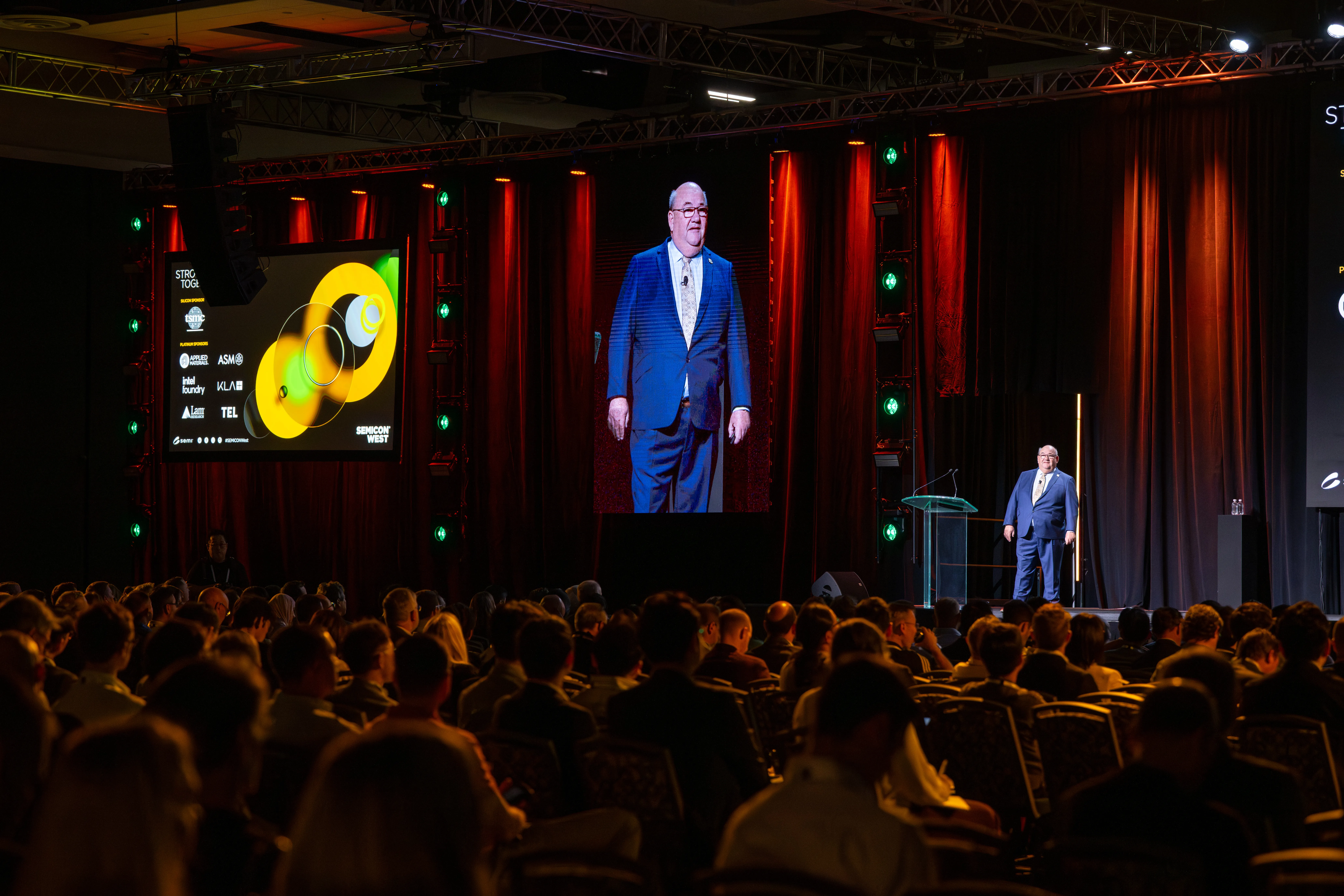
SEMICON West 2025 marked a year of many milestones. Not only was it the first SEMICON West ever to take place outside of San Francisco Bay Area, but it was also its largest exhibition in over 18 years. This year saw a 45% increase in booths, along with a 60% surge in registrations over 2024. The CEO Summit Keynote Series also returned to SEMICON West, featuring 14 unique presentations from October 7-9 at Arizona’s Phoenix Convention Center. Top leaders from both government and industry shared insights on a range of pertinent topics, from technology innovations, to emerging partnerships, sustainability and supply chain initiatives, and more. The keynote series began with opening remarks from SEMI’s President and CEO, Ajit Manocha, who urged audience members to focus on strategies that drive the industry forward and reinforced the importance of collaboration. He also outlined SEMI’s current priorities, including mitigating talent shortages, environmental disruptions, and geopolitical volatility.For those who missed the CEO Summit Keynote Series, this blog offers a summary of each presentation. The State of Arizona“In Arizona, vision becomes opportunity, and opportunity becomes action.” – Katie HobbsSEMICON West’s keynote series kicked off with Arizona Governor, Katie Hobbs, who underscored the expansive growth of Arizona’s semiconductor industry. She highlighted TSMC’s $165 billion investment in Arizona, the largest foreign direct investment in the state’s history, as well as more than 60 other semiconductor expansions that have taken place in the state. There are several reasons, Hobbs said, why Arizona has become an attractive place for semiconductor companies. The local talent base is one, with Arizona ranking among the top five states in the country in this area. Hobbs also highlighted Phoenix’s reliable energy grid, pro-business climate, and 100-year plan for water.AI in Every Layer: Future-Ready Strategies for Technology and Talent“This much disruptive innovation can’t be done by any one company. It requires a broad collaboration ecosystem.” – Sesha Varadarajan Following Hobbs, Sesha Varadarajan from Lam Research discussed AI-related challenges and budding solutions that address them. With AI setting the pace of industry innovation, Varadarajan emphasized the need for clarity for device-specific roadmaps. For example, logic is transitioning from FinFET to Gate-All-Around, DRAM is moving toward 3D architectures, and advanced packaging innovations are enabling continued scaling. Ultimately, Varadarajan concluded that device roadmaps would come down to three things: thinner materials, taller structures, and smaller features. Lastly, he noted that workforce development training often lags behind industry demand, highlighting Lam Research’s Semiverse education platform as a solution. Stronger Together - Building a Resilient Future for Semiconductors“When you’re working at an atomic level of precision, every detail matters.” – Jon KempDupont’s Jon Kemp offered insight into how the semiconductor industry can usher in a new wave of transformation. To achieve this, he highlighted three strategic priorities: supply chain, sustainability, and AI. Kemp emphasized bringing manufacturing closer to customers, designing products for energy efficiency, and creating new AI architectures that address mounting performance expectations. He also announced that Qnity, an integrated material solutions provider, will be spinning out of DuPont on November 1, 2025. Where Vision Meets Execution: Global Executive Summit (GES) Unites Industry Leaders“[There has been] lots of progress so far, and we want to build on that momentum.” – Carolin Seward. Carolin Seward from Google took the stage to discuss the upcoming Global Executive Summit (GES) from December 15-16 in Tokyo. This invitation-only meeting will convene industry executives to discuss core sustainability issues, like advancing abatement, pursuing gas substitution, driving green materials, and enabling low-carbon energy. Closer to Home: Costa Rica as a Partner for Successful Operations in the Western Hemisphere“Costa Rica is ready to become part of the solution.” – Manuel Tovar RiveraManuel Tovar Rivera discussed Costa Rica’s efforts to bolster its semiconductor industry. With its close proximity to the U.S., three decades of advanced manufacturing experience, and free trade, Rivera also explained the benefits of U.S. and Costa Rica collaborations. To meet the needs of its trade partners, Costa Rica is developing its local talent base, attracting foreign professionals, offering incentives for R D and startup investment, and streamlining its regulatory processes. Advancing 3DIC Technologies to Propel AI Innovations“Our best day is still ahead of us.” – Jun HeClosing out the Tuesday keynote series was TSMC’s Jun He, who spoke about the packaging innovations that are pushing the world closer to more advanced AI. The key benefit of advanced packaging, he said, is to enhance AI performance and efficiency–but excellent yield is a nonnegotiable requirement. He underscored the growing importance of CoWoS, or Chip-on-Wafer-on-Substrate packaging structures, as well as fluxless thermocompression bonding, to help meet demand for AI. AI Supercomputing for Next Generation Semiconductor Design and Manufacturing“AI factories transform electricity into intelligence.” – Timothy CostaNIVIDA’s Timothy Costa began the Wednesday keynote series by highlighting physical AI as “the next trillion-dollar industry,” and outlined how the company is helping the industry get closer to that benchmark. Costa noted the three NVIDIA computers being used to train physical AI models – Omniverse for simulation, DGX for training, and Jetson AGX for deployment. All of these, he said, need to work together to deliver on physical AI promises, like robotics, autonomous vehicles, and others. Executive Panel – Powering the Next Decade: AI’s Impact on Semiconductor Infrastructure and Market“We’re living in the most exciting time in the world of computing.” – Mukesh KhareFollowing Costa, the CEO Summit Keynote stage transitioned into a panel discussion with industry-leading AI experts – including Laura Matz from Merck KGaA, Darmstadt, Germany, Mukesh Khare from IBM Research, Mark Dougherty from TEL, and Angada Sachid from ASM. The panel was moderated by David Anderson, President of NY CREATES. Although there was much said during this 50-minute panel, a few key points were emphasized. First, Khare highlighted open chip design activities for AI models as a way to alleviate cost burdens. Design costs for more advanced nodes, he said, can be greater than $500 million. Matz also outlined the urgent need to develop PFAS-free materials without sacrificing yield. Currently, there are several areas where the industry doesn’t have a solution for PFAS, but AI models may be able to help.Sachid also mentioned power challenges, pointing to how one or two misplaced atoms can be the difference between a power-efficient versus a power-hungry chip. Deposition needs to be perfect at 10 trillion separate locations, and he pointed to AI as an emerging solution for this as well. However, despite the promises of AI, the panelists underscored that people are still a company’s most valuable asset. Revolutionizing Semiconductor Collaboration: The Emergence of AI-Driven Industry Platforms“You can make better decisions with more information.” – John KibarianWhile nearly every session touched on the need for industry-wide collaboration, John Kibarian from PDF Solutions focused on making this feasible. In today’s highly complex semiconductor supply chain, every point is critical, from fabless companies, to foundries, OSATs, and external vendors. To make industry-wide collaboration practical without compromising IP, he noted the importance of secure infrastructure, automated orchestration, and robust AI agents to assess and analyze the raw data that often goes unused. Kibarian highlighted PDF Solutions’ secureWISE system as a tool that’s already in place to address these needs. Shaping the Future of Semiconductors in the U.S.“The specific things that drove growth were the evolution of new applications.” – Giel RuttenAs the semiconductor industry continues its journey to $1 trillion in annual industry revenue, Amkor’s Giel Rutten provided an update on the U.S. market. Because OSATs are heavily concentrated in Asia, this poses a significant challenge for reshoring U.S. manufacturing. Most OEMs, he said, are looking to OSATs to handle several of their processes because it’s cheaper than doing it themselves. Rutten detailed the mounting complexities of backend assembly, including rising demand for multiple, high-bandwidth memory stacks that traditional SoCs can’t accommodate. This is pushing the industry toward heterogeneous integration, which further complicates the supply chain. Rutten concluded by emphasizing the importance of industry-wide collaboration, and noted that Amkor’s Arizona fab will offer a complete, turnkey supply chain in the U.S. Fireside Chat – Harnessing Digital Transformation to Empower People and Accelerate Precision“The more we double down on technology, the more we should also elevate humanity and double down on our values.” – Khadija Ben HammadaWith a strong emphasis on AI during the 2025 keynote series, the final discussion on Wednesday brought humans back into the spotlight. Khadija Ben Hammada from Merck KGaA, Darmstadt, Germany and Daniel Drellich from EMD Electronics (the electronics business of Merck KGaA, Darmstadt, Germany), joined Jon Krohn on stage for an insightful talk on empowering employees in today’s AI era. Of the many things discussed, both Hammada and Drellich underscored the need to build trust with employees, as many of them fear being left behind by the technology. While it’s true that companies have invested heavily in AI, such investments also require them to educate teams on how to use it. This can best be achieved through a culture, they said, where people feel comfortable enough to learn in the first place. The panelists also highlighted the importance of finding the right AI tools for specific purposes, instead of blindly choosing the most sophisticated solution. Partnering to Serve the Demands of the AI Era“A foundry business is a trust business.” – Kevin O’BuckleyAlthough there’s no shortage of discussion about the industry’s road to $1 trillion, Intel’s Kevin O’Buckley shared where that trillion-dollar value is being realized. Based on recent projections, the simple breakdown he presented shows that 50% is generated by fabless companies, 25% by suppliers, and 25% by foundries and OSATs. With the rise of fabless companies, he highlighted the need for foundries to provide value to customers, including better power delivery solutions and predictable execution on customer projects. He also shared Intel’s efforts, like bringing its 18A node into production, its PowerVia for backside power delivery, and new slurry formulations for delicate wafers. Bridging the Talent Gap: Accelerating Workforce Solutions for Semiconductors“We're building opportunity and innovation into the semiconductor workforce.” – Shari LissShari Liss, VP of Global Workforce Development and Initiatives at SEMI, detailed the current state of the industry’s workforce needs. More than 170,000 new workers, she said, will be needed in the U.S. in the next five years. To help close the talent gap, Liss shared a roadmap of the SEMI Foundation’s efforts, ranging from awareness programs that target children as young as seven, to apprenticeship programs for adults. So far, the SEMI Foundation has reached 1.25 million students through its apprenticeship and certification programs, 3,300 people through its expanded childcare access, and 7,000 people through its SEMI U courses. Liss also highlighted the SEMI Foundation’s operator role in the newly established National Network of Microelectronics Education (NNME) — a national program that aims to build regional centers around the U.S. for microelectronics education and training. Requests for proposals are now open, and applications are due in December. American Chip Revival and the Trusted Tech Imperative“Trust is the most important word in any language.” – Keith KrachThe 2025 keynotes series concluded with Purdue University’s Keith Krach and former undersecretary of state. During his time as undersecretary, he emphasized the importance of building trust to rebuild the U.S. semiconductor supply chain. Through his trust-first approach, Krach helped secure TSMC’s presence in Arizona, leading to better jobs and a stronger domestic chip ecosystem. In addition, he was instrumental in creating a clean 5G network that later became the xGTT, or the Global Trusted Tech Standard. SEMI would like to thank all speakers, sponsors, and attendees for the success of this year’s CEO Summit Keynote Series. Joe Stockunas is President, SEMI Americas.
Read More
The Department of Commerce (DOC) has issued an amended version of the semiconductor supply chain Notice of Funding Opportunity (NOFO), commonly referred to as “NOFO 2.” This NOFO is explicitly geared toward projects that would construct, expand, or modernize semiconductor materials facilities or semiconductor manufacturing equipment facilities. Initial concept plans will be accepted until November 1, 2026. DOC released the first version of NOFO 2 in September 2023. While the amended version maintains the focus on upstream suppliers of semiconductor manufacturing materials and equipment, it differs in several key aspects from the original. Outside of the application deadline extension, some of the most notable differences include the following.Project Cost: The amended NOFO 2 removes the $300 million cap on individual projects but argues that individual projects under $20 million are unlikely to reach a scale necessary for achieving strategic objectives.Cost Sharing: The amended version lacks a cost sharing requirement but notes that individual applicants "must be able to demonstrate that they have sufficient resources available to complete the proposed project, when combined with the requested CHIPS Incentives."Fab Clusters: NOFO 2 includes a focus on supporting "the development of vibrant, sustainable semiconductor clusters" by, for example, "reducing the burdens associated with transporting critical supply chain inputs." Evaluation Criteria: Proposals will be evaluated using the following five criteria:Economic and National SecurityCommercial ViabilityFinancial StrengthProject Technical Feasibility and ReadinessWorkforce Development Available Funding: The amended NOFO 2 does not specify a total amount of available funding, which is a departure from the September 2023 version, which set aside $500 million for the entire endeavor. Eligible Applicants: Eligible applicants include private sector organizations, non-profit organizations, consortia of private sector organizations, and consortia of private, public, and/or nonprofit organizations “with a demonstrated ability to substantially finance, construct, expand, or modernize a facility relating to the fabrication, assembly, testing, advanced packaging, production, or research and development of semiconductors, materials used to manufacture semiconductors, or semiconductor manufacturing equipment.”Application Structure and Deadlines: Initial concept plans will be accepted until November 1, 2026. DOC will notify applicants that have been invited to submit full proposals on an individual basis. Sources and Additional Information:NOFO 2NOFO 2 FAQ Visit SEMI Global Advocacy to learn more about public policy efforts and developments as well as how your company or organization can get involved.Ben Kallen is Sr. Manager, Public Policy Advocacy at SEMI.
Read More
On Friday, September 19, 2025, the President signed a proclamation requiring a new $100,000 fee for United States H-1B visa applications effective September 21, 2025 seeking to curb what the administration views as significant overuse. A memorandum later issued by the United States Citizenship and Immigration Services (USCIS) Director clarified that the fee applies only to new, unfiled petitions. Current visa holders can continue traveling to and from the United States.While SEMI recognizes the economic and strategic concerns raised by the administration, the high cost of the new fee poses a significant burden on SEMI members and the broader technology industry. As SEMI members continue to share the impact this policy will create on their operations, SEMI will work with fellow trade associations to address the high-cost of the fee and find solutions for the administration’s policy concerns.The proclamation cites misuse and calls "abuse of the H-1B program" a "national security threat." All entries under an H-1B visa beginning September 21, 2025, are restricted unless supplemented by the $100,000 payment. The administration must review this restriction annually, and DHS will issue implementation guidance. The proclamation also directs DHS to revise prevailing wage levels and prioritize "high-skilled and high-paid" applicants.The H-1B program currently caps new visas at 65,000 annually, plus 20,000 for those with U.S. master's degrees or higher. Employers must petition for these visas. Demand for skilled workers—especially in technology-driven industries like semiconductors—far exceeds the limited H-1B supply. The changes risk driving away U.S.-educated foreign graduates and their skills to foreign markets, further straining workforce needs.SEMI recognizes the impact of the proposed H1-B visa fee on companies, particularly the additional burden it places on smaller firms. While SEMI supports the administration’s objectives, the policy will create near-term challenges — especially for companies working to scale in order to meet the goals set by Congress and the administration to strengthen economic and national security. By straining the talent and resources these companies rely on, the fee risks undermining those objectives.In the coming days, SEMI will be gathering information to better understand the impact across the industry, with particular attention to smaller companies. This input will guide our communications with the administration as it refines the policy. We will also be meeting with member companies to assess the impact and prepare talking points for upcoming discussions with the administration.Next Steps: SEMI issued an initial statement recognizing the administration's economic and security concerns while urging collaboration on solutions that benefit economic growth and talent retention. SEMI will work with industry groups, the administration, and Congress to address H-1B challenges and help grow the American workforce while retaining global talent. SEMI is spearheading a letter to the administration highlighting industry concerns while expressing the desire to work together, and we will be inviting related industry associations and groups to join us. SEMI encourages members to share details on the anticipated impact of the policy on their operations. Please reach out to Christina Banoub at [email protected] policy aligns with forthcoming H-1B rulemaking that would weigh applications by wage levels instead of the current lottery system. The rule hasn't yet appeared in the Federal Register but should follow soon.Visit SEMI Global Advocacy to learn more about public policy efforts and developments as well as how your company or organization can get involved.Royal Kastens, Senior Director of Public Policy and Advocacy at SEMI.
Read More
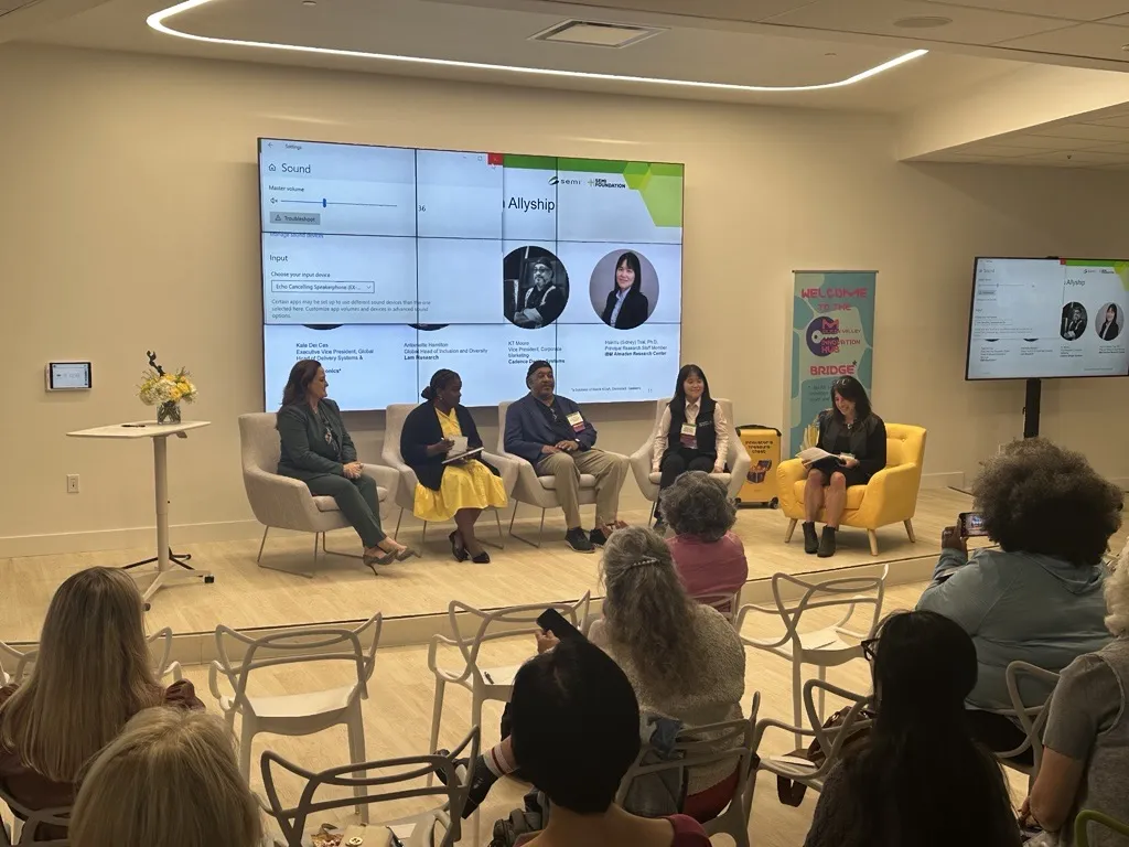
This year, the Women in Semiconductor (WiS) program takes a huge step growing nationally — hosting events in New York, Michigan, Ohio, California, and Arizona. Managed by the SEMI Foundation, the WiS program aims to highlight women’s contributions and leadership in the semiconductor sector and actively address the gender gap to support inclusive workplaces.Over the years, WiS has shifted from an abstract discussion to actionable strategies—focusing on skills like negotiation, strategic decision-making, storytelling, and career advancement. WiS also promotes allyship, inviting and including men to participate as advocates and supporters of women in the industry.Building on the program’s strong momentum, this year highlights the initiative’s growth and impact through expansion across multiple regions – focusing on the theme “Empowerment in Action: Real Strategies for Women’s Success” dedicated toward impactful, actionable programming.The first 2025 WiS program was held in Albany, NY, in conjunction with ASMC on May 8. New WiS programs are scheduled in the following locations:Ann Arbor, Michigan on September 16, 2025Willoughby, Ohio (date to be announced)San Jose, CA on November 20, 2025Phoenix, Arizona on December 11, 2025The WiS is supported by grants from the Kellogg Foundation and the David Lucile Packard Foundation. The programming is also aligned with SEMI Foundation’s Chips Childcare program, which supports childcare-access solutions to strengthen workforce participation—particularly for parents and caregivers. Learn more in our blog: Affordable, Accessible, and Quality Childcare: A Critical Workforce Development Strategy for the Semiconductor Industry.The WiS initiative has evolved into a powerful platform that blends strategic programming, mentorship, allyship, regionally accessible events, and support systems like childcare advocacy. It’s an inspiring example of how consistent focus and innovation can build meaningful change over nearly a decade. If you’re interested in getting involved, contact Bia Hamed at [email protected]. Bia Hamed, Ph.D., is Program Manager for Global Education Initiatives at the SEMI Foundation, focusing on educational programming that supports workforce pipeline building nationally and internationally.
Read More
As the Department of Commerce explores options to adjust patent fees, these changes will have important implications for the semiconductor industry, where thousands of patents are filed each year to protect groundbreaking technologies. At SEMI, we understand the complexity of getting this right for our member companies. The fee proposal is not only about rates, but also about how fees are structured, applied across different types of filers, and administered in practice. Designing a system that is fair and workable is a significant challenge and one that requires close collaboration between government and industry. The SEMI Global Advocacy team is consistently engaged with the Trump Administration and Congress as a resource. We want to ensure the unique needs of the semiconductor sector are understood and that any adjustments to the fee schedule strengthen U.S. innovation without creating unintended barriers. By working together, SEMI members with U.S. operations can help shape an approach that supports the U.S. Patent and Trademark Office's mission and U.S. competitiveness. Next Steps: SEMI will continue to provide technical insight from across our membership as this process develops and looks forward to partnering with policymakers. We will also share updates as information on new patent fees become available beyond the initial reporting by the Wall Street Journal and other news outlets.Visit SEMI Global Advocacy to learn more about public policy efforts and developments as well as how your company or organization can get involved.Scarlett Bickerton, Manager, Federal State Affairs at SEMI.
Read More
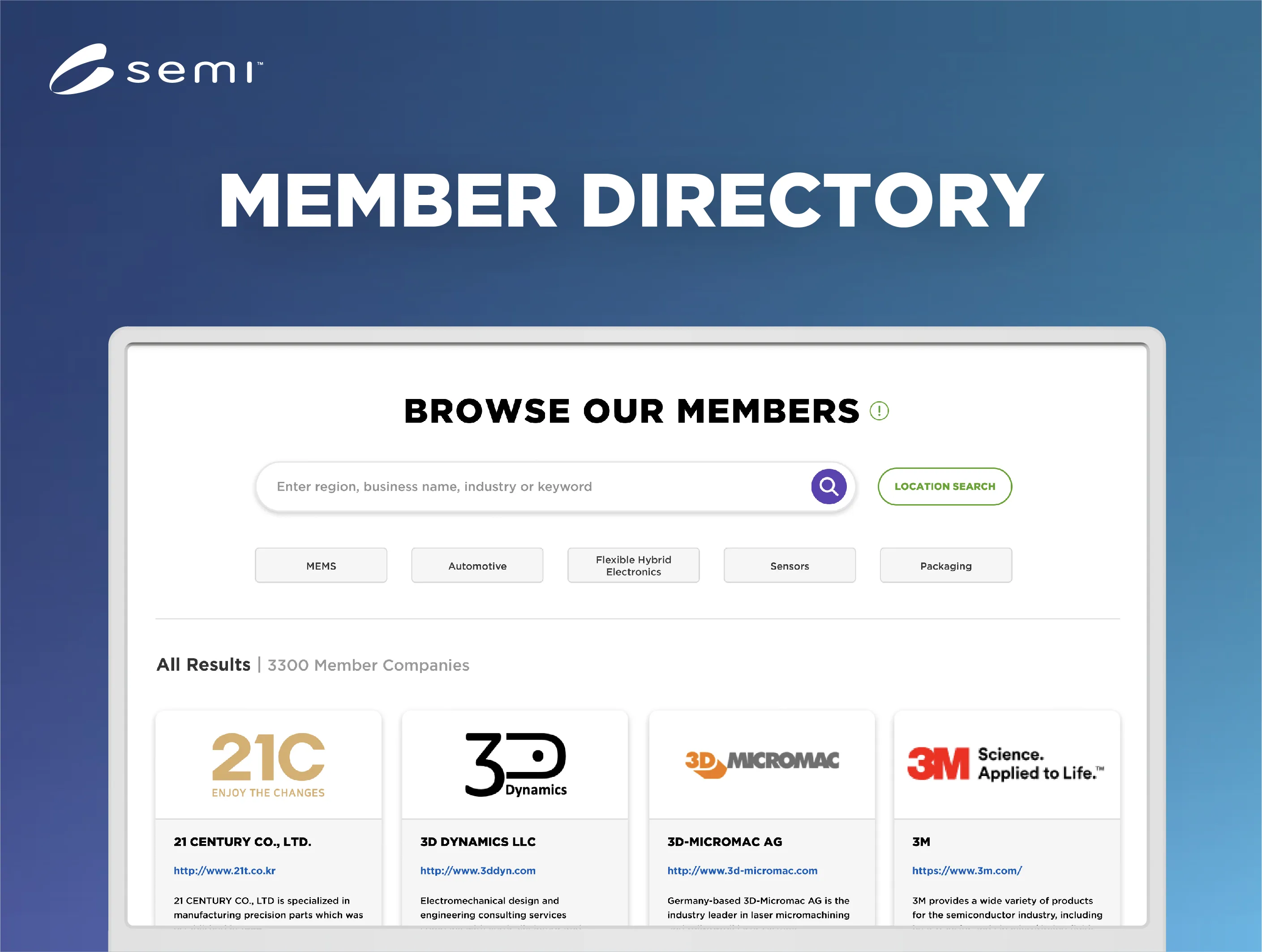
SEMI members span the entire semiconductor manufacturing supply chain, representing diverse industry segments, product offerings, geographic regions, company sizes, and ownership types. The SEMI Member Directory serves as a key resource that showcases companies across the microelectronics value chain while helping to amplify their brands. We’re excited to announce recent enhancements to our member directory that include a refreshed design, improved search functionality, and more up-to-date company information.WHAT’S NEWClean Look FeelDefault “tile view” display of member companiesCompany profile pages with English and optional local-language contentAbility to display up to 48 companies per page viewSmart Search Functionality Searches scan all company profile descriptions, keywords, and location detailsSearches support all languagesIndustry-focused results limited to the semiconductor manufacturing supply chainMember Company Access Primary member contact can instantly update their company’s directory information, including:Business overviewCompany logo uploadAdditional search keywordsWHY IT MATTERSThe Member Directory averages 15,000-20,000 active viewers each month, providing a powerful platform to boost your company’s visibility within the industry. Combined with SEMI’s reputation and reach, it’s an effective way to be seen by the right audience.LOOKING AHEADWe’re not done yet. SEMI will continue to improve and enhance the directory with additional upgrades in the coming months. Check out the new directory and see the latest improvements. If your organization isn’t yet among our 3,000+ member companies, now is the perfect time to join our global community. Learn more by submitting a membership inquiry form or contact a regional office.Eric Thoe is Senior Director, Member Services at SEMI.
Read More
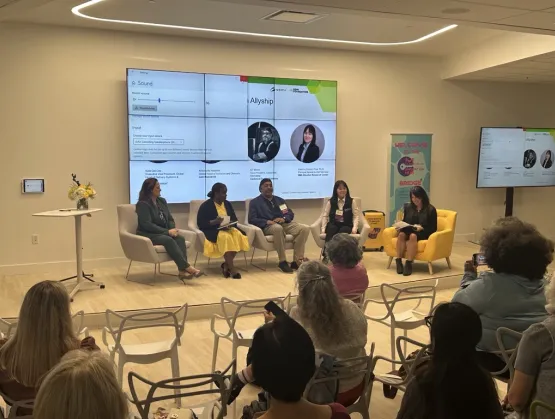
“In today's ever-evolving professional landscape, empowering women and fostering their success is not just necessary—it's essential," said Caryn Veach, a long-time Women in Semiconductors (WiS) committee member. Veach is a strategic account manager at Kokusai Electric Corporation, which sponsored the WiS program in Albany, New York in May. Additional sponsors included Axcelis, Energetiq (a Hamamatsu Company), IBM, Nikon Precision and Onto Innovation.This year’s WiS theme, "Empowerment in Action: Real Strategies for Women’s Success," was designed to provide all attendees with actionable strategies to support women's career growth and representation, as well as lead to greater talent retention and workforce stability. The program, which was open to everyone at the co-located SEMI Advanced Semiconductor Manufacturing Conference, was co-chaired by Joy Racowski, PhD., Strategic Account Sales Engineering Manager - Delivery Systems Services at EMD Electronics and Rosanna Robert, ES Process Engineer ll at TEL Technology Center America.Keynote speaker Jennifer Lynn, Cybersecurity Leader and Research Security Program Manager at IBM Semiconductors emphasized the significance of community in driving change. She stressed the role of Employee Resource Groups (ERGs) as a collective voice to advocate for safer and welcoming workspaces where all individuals feel respected and valued. Some key takeaways from Lynn’s address: champion supportive career initiatives, become a mentor or find a mentor, and be an ally in support of peer success. Shari Liss, Vice President of Global Workforce Development and Initiatives at SEMI, moderated a panel which also highlighted real strategies for women’s success. Panelists from EMD Electronics, Entegris, TEL Technology Center of America and University at Albany focused on actionable strategies which everyone, not only women, can implement to navigate corporate environments. They encouraged WiS participants to challenge norms which penalize specific employees. Panelists invited attendees to discover and embrace what makes them unique and use that as a strength for themselves as well as others. (l-r) WiS panel: Shari Liss, SEMI; Jennifer Braggin, Director, Technology, Office of the CTO, Entegris; Daniel Drellich, Managing Director Sr. Vice President of Business Partnering, EMD Electronics; Kathleen Dunn, PhD, Professor of Nanoscale Science and Engineering, University at Albany; Alex Oscilowski, President, TEL Technology Center AmericaImposter Syndrome is a common challenge to women and those who are new in their career or leadership role. Panelists advised everyone to push through it and support others who might feel this way. Assertiveness is an area which should be seen as a strength rather than a disadvantage, especially for women; it’s important that different voices and opinions are heard. Finally, panelists urged everyone to give credit where it is due and actively support team members and peers.The program concluded with an interactive workshop facilitated by Debbie Gustafson, CEO of Energetiq Technology. Attendees were invited to craft an elevator pitch which could be used when networking or applying for a new job or position. Common elements of a pitch include a concise description of oneself, a unique value proposition and a call to action for one’s audience or employer. WiS was an empowering experience with excellent opportunities to network with female business leaders from around the country as well as recent college graduates and industry professionals from major semiconductor manufacturers. There is something uniquely impactful about coming together with other women and peers who understand the challenges and opportunities of our industry. These events create space for honest conversations, meaningful networking, and a sense of community. It is a reminder that that together we can drive change and support one another in powerful ways. Through grants from the W.K. Kellogg Foundation and the David Lucille Packard Foundation, the SEMI Foundation is expanding Women in Semiconductors programming to several regions around the country. In addition to an event in San Jose, California there will be programs in Arizona, Michigan and Ohio in the second half of 2025. For information on WiS in Michigan, visit https://semiscan.org/event/women-in-semiconductors/.Empowering women in the workplace requires persistent effort and community support. By embracing these strategies and advocating for necessary changes, organizations can pave the way for a more equitable future. And just like the Kokusai Electric embrace of Tai-wa, a Japanese word meaning "synergistic discourse", WiS encourages face-to-face conversations and a willingness to understand others with a sense of empathy and respect for everyone.Margaret Kindling is Senior Program Manager at the SEMI Foundation. She has promoted inclusive workplaces via initiatives like WiS, Semiconductor PRIDE and workforce development programming at SEMICON West, SEMICON India and SEMIEXPO Heartland. After a combined 37 years at SEMI and the SEMI Foundation, she will be retiring in August 2025.
Read More